 | –≠–ª–µ–∫—Ç—Ä–æ–Ω–Ω—ã–π –∫–æ–º–ø–æ–Ω–µ–Ω—Ç: D372A | –°–∫–∞—á–∞—Ç—å:  PDF PDF  ZIP ZIP |

2
Supply voltage
Operating range
V+
2.0
6.5
V
E = V+
Withstand range
-0.5
9.0
E = GND
Enable Voltage
E
-0.5
(V+) +0.5
V
Lamp Output
Vout
220
Vpp
E = V+
Operating temperature
T
a
-40
85
∞C
Storage temperature
T
s
-65
150
∞C
Load A*
Physical Data:
PIN # NAME
FUNCTION
Absolute Maximum Ratings:
Note: The above are stress ratings only. Functional operation of the device at these ratings or any other above
those indicated in the specifications is not implied. Exposure to absolute maximum rating conditions for extended
periods of time may affect reliability.
Parameter
Symbol
Minimum
Maximum
Unit
Comments
1
V+
DC power supply input
2
CLF
Low frequency oscillator capacitor/LF clock input
3
CHF
High frequency oscillator capacitor/HF clock input
4
E
System enable: HI = On
5
GND
System ground connection
6
L+
Charge pumping inductor input
7
Cs
High voltage storage capacitor
8
EL1
AC output to lamp
9
EL2
AC output to lamp
10
Rd
Wave shaping resistor
* Load A approximates a 3in
2
EL lamp.
1
2
3
4
5
10
9
8
7
6
100
10 nF
Sample Output Waveform

3
Typical Performance Characteristics Using Standard Test Circuit
Output Frequency vs. DC Supply Voltage
0
50
100
150
200
250
300
350
400
1
2
3
4
5
6
7
DC Input Voltage
LF (Hz)
0
50
100
150
200
250
300
350
400
-40
-20
0
20
40
60
80
Temperature (
o
C)
LF (Hz)
Output Frequency vs. Ambient Temperature
0
50
100
150
200
250
300
1
2
3
4
5
6
7
DC Input Voltage
Output Voltage (Vpp)
Output Frequency vs. DC Supply Voltage
0
50
100
150
200
250
300
-40
-20
0
20
40
60
80
Temperature (
o
C)
Ouput Voltage (Vpp)
Output Frequency vs. Ambient Temperature
0
5
10
15
20
25
1
2
3
4
5
6
7
DC Input Voltage
Avg Supply Current (mA)
Output Frequency vs. DC Supply Voltage
0
5
10
15
20
25
-40
-20
0
20
40
60
80
Temperature (
o
C)
Avg Supply Current (mA)
Output Frequency vs. Ambient Temperature

4
Theory of Operation
Electroluminescent (EL) lamps are essentially capacitors with one transparent electrode and a special phosphor material
in the dielectric. When a strong AC voltage is applied across the EL lamp electrodes, the phosphor glows. The
required AC voltage is typically not present in most systems and must be generated from a low voltage DC source.
The D372 chip inverter drives the EL lamp by using a switching BJT to repeatedly charge an external inductor and
discharge it to the high voltage capacitor Cs. The discharging causes the voltage at Cs to continually increase. When
the voltage at Cs reaches a nominal value, the switching BJT is turned off. The internal circuitry uses the H-bridge
technology, using both electrodes to drive the EL lamp. One of the outputs, EL1 or EL2, is used to discharge Cs into the
EL lamp during the first half of the low frequency (LF) cycle. By alternating the state of the H-bridge, the other output
is used to charge the EL lamp during the second half of the LF cycle. The alternating states make it possible to achieve
200V peak-to-peak across the EL lamp.
The EL driving system is divided into several parts: on-chip logic control, on-chip high voltage output circuitry, on-chip
discharge logic circuitry, and off-chip components. The on-chip logic controls the lamp operating frequency (LF) and
the inductor switching frequency (HF). These signals are used to drive the high voltage output circuitry (H-bridge) by
delivering the power from the inductor to the lamp. The integrated discharge logic circuitry uses a patented wave
shaping technique for reducing audible noise from an EL lamp. Changing the Rd value changes the slope of the linear
discharge as well as the shape of the waveform. The off-chip component selection provides a degree of flexibility to
accommodate various lamp sizes, system voltages, and brightness levels.
Typical D372 EL driving configurations for driving EL lamps in various applications are shown on the following page.
The expected system outputs for the various circuit configurations are also shown with each respective figure. These
examples are only guides for configuring the driver. Durel provides a D372 Designers Kit, which includes a printed
circuit evaluation board intended to aid you in developing an EL lamp driver configuration using the D372 that meets
your requirements. A section on designing with the D372 is included in this datasheet to serve as a guide to help you
select the appropriate external components to complete your D372 EL driver system.
Block Diagram of the Driver Circuitry
'
EL Lamp
E
V+
L+
GND
EL1
High
Frequency
Oscillator
CHF
Low
Frequency
Oscillator
CLF
R
d
V
BAT
L
o
g
i
c
L
o
g
i
c
Divide
by 2
EL2
C
S

5
Typical D372A EL Driver Configurations
3.0V Handset LCD
Typical Output
Brightness = 6.0 fL (20.6 cd/m
2
)
Lamp Frequency = 285 Hz
Supply Current = 12 mA
Vout = 208 Vpp
Load = 1 in
2
(645 mm
2
) Durel
Æ
3
Green EL
5.0 V LCD Backlight
Typical Output
Luminance = 6.0 fL (24.3 cd/m
2
)
Lamp Frequency = 300 Hz
Supply Current = 22 mA
Vout = 206 Vpp
Load = 4 in
2
(2580 mm
2
)Durel
Æ
3
Green EL
3.3 V Handset LCD and Keypad
Typical Output
Luminance = 5.5 fL (18.8 cd/m
2
)
Lamp Frequency = 290 Hz
Supply Current = 17 mA
Vout = 200 Vpp
Load = 1.5 in
2
(950 mm
2
)Durel
Æ
3
Green EL
V+
CLF
CHF
E
GND
Rd
EL2
EL1
Cs
L+
D372A
1.5 in
2
EL Lamp
Murata
LQH3KS
2.2 mH
47 nF
1.0 k
68 pF
2.0 nF
0.1
µ
F
+3.3 V
1
2
3
4
5
10
9
8
7
6
+3.3 V
0 V off
on
3.3 V
V+
CLF
CHF
E
GND
Rd
EL2
EL1
Cs
L+
D372A
4.0 in
2
EL Lamp
Sumida
CLS62
1.5 mH
47 nF
220
68 pF
2.0 nF
0.1
µ
F
+5.0 V
1
2
3
4
5
10
9
8
7
6
+5.0 V
0 V off
on
5.0 V
V+
CLF
CHF
E
GND
Rd
EL2
EL1
Cs
L+
D372A
1.0 in
2
EL Lamp
Bujeon
BDS-3516S
1.5 mH
47 nF
1.0 k
68 pF
2.0 nF
0.1
µ
F
+3.0 V
1
2
3
4
5
10
9
8
7
6
+3.0 V
0 V
off
on
3.0 V
6
Designing With D372
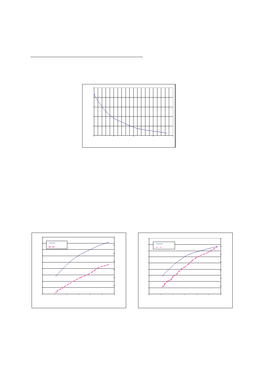
I. Lamp Frequency Capacitor (CLF) Selection
Selecting the appropriate value of capacitor (CLF) for the low frequency oscillator will set the output frequency of the
D372 inverter. Figure 1 graphically represents the effect of the CLF capacitor value on the oscillator frequency at
V+ = 3.0V.
The lamp frequency may also be controlled with an external clock signal. The resulting lamp frequency will be half of
the clock signal frequency. The differential output voltage will increase in magnitude during the high portion of the
clock signal and decrease during the low portion of the clock signal. Lamp frequencies of 200-500Hz are typically
used.
The selection of the CLF value can also affect the output brightness and current consumption of the driver. The EL
lamp frequency (LF) depends on lamp size, drive conditions, and mainly on the CLF value selected. Figures 2 and 3
show typical brightness and current draw of a D372 circuit at different frequencies. The data was taken with an
average 1.0mH inductor and 68 pf CHF capacitor.
Figure 1: Typical Lamp Frequency vs. CLF Capacitor
Figure 2: Typical Luminance and Current
vs. Lamp Frequency
Conditions: V+ = 3.0 V, 1.5 in
2
EL Lamp
Figure 3: Typical Luminance and Current
vs. Lamp Frequency
Conditions: V+ = 5.0 V, 4.0 in
2
EL Lamp
100
200
300
400
500
600
1
2
3
4
5
CLF (nF)
Lamp Frequency (Hz)
0
1
2
3
4
5
6
7
8
9
0
100
200
300
400
500
600
Frequency (Hz)
10
15
20
25
30
35
40
45
Luminance
Current
Luminance (fL)
Current (mA)
0
1
2
3
4
5
6
7
8
9
0
100
200
300
400
500
600
Frequency (Hz)
10
15
20
25
30
35
40
45
Luminance
Current
Luminance (fL)
Current (mA)

7
Selecting the appropriate value of capacitor (CHF) for the high frequency oscillator will set the inductor switching
frequency of the D372 inverter. Figure 4 graphically represents the effect of the CHF capacitor value on the oscillator
frequency at V+ = 3.0V.
Figure 4: Typical Inductor Frequency vs. CHF Capacitor
The inductor switching frequency may also be controlled with an external clock signal. The inductor will charge
during the low portion of the clock signal and discharge into the EL lamp during the high portion of the clock signal.
II. Inductor Switching Frequency (CHF) Selection
III. Inductor (L) Selection
The inductor value and inductor switching frequency have the greatest impact on the output brightness and current
consumption of the driver. Figures 5 and 6 show typical brightness and current draw of a D372 circuit with several
different inductor and CHF values. The CLF value was modified in each case such that the output voltage was
approximately 200Vpp. The data was taken with average inductors. Please note that the DC resistance (DCR) and
current rating of inductors with the same inductance value may vary with manufacturer and inductor type. Thus,
inductors made by a different manufacturer may yield different outputs, but the trend of the different curves should be
similar.
Figure 5: Luminance and Current
vs. Inductor and CHF Value
Conditions: V+ = 3.0 V, 1.5 in
2
EL Lamp
Figure 6: Luminance and Current
vs. Inductor and CHF value
Conditions: V+ = 5.0 V, 4in
2
EL Lamp
10
15
20
25
50
75
100
125
150
175
200
CHF (pF)
Inductor Frequency (KHz)
0
1
2
3
4
5
6
7
8
9
0.0
1.0
2.0
3.0
4.0
5.0
6.0
CLF (nF)
10
15
20
25
30
35
40
45
50
68 pF Luminance
100 pF Luminance
68 pF Current
100 pF Current
Luminance (fL)
Current (mA)
0
1
2
3
4
5
6
7
8
9
0.0
1.0
2.0
3.0
4.0
5.0
6.0
CLF (nF)
10
15
20
25
30
35
40
45
50
68 pF Luminance
100 pF Luminance
68 pF Current
100 pF Current
Luminance (fL)
Current (mA)

IV. Wave-Shape (Rd) Selection
The R
d
resistor determines the slope of the charge and discharge portions of the output waveform. The optimal value
of this resistor depends on the lamp size and drive conditions. Typical values range from 0
- 2.0k
. Recommended
starting values for various lamp sizes are shown in the table below. The optimal waveform is trapezoidal which will
result in the best combination of high brightness and low audible noise performance. Using a larger value of Rd than
recommended will result in a triangular waveform and correspond to reducing the audible noise of the EL lamp and
increase lamp life. However, the luminance of the EL lamp will decrease. Using a smaller value of Rd than recom-
mended will result in a square waveform and correspond to higher initial luminance from the EL lamp, but will not take
advantage of the noise reduction capability of the D372.
Typical waveforms corresponding to the selected R
d
values for a 2in
2
lamp and a 4in
2
lamp are shown below.
Rd = 820
Optimal waveform for 2 in
2
Rd
Lamp Size
1.2k
<1.0 in
2
820
1.0-2.0 in
2
470
2.0-4.0 in
2
220
>4.0 in
2
Lamp Size 2 in
2
Rd = 1.2k
Reduced noise with lower luminance
Rd = 470
Optimal waveform for 4 in
2
Lamp Size 4 in
2
Rd = 0
Higher luminance with more noise
8

V. Storage Capacitor (Cs) Selection
The Cs capacitor is used to store the energy transferred from the inductor. Capacitors with larger values have a larger
time constant and will store the energy for longer periods of time. The recommended Cs values range from 10nF to
47nF and are to be rated to at least 100V. Larger EL lamps typically require larger values of Cs. In general, increasing
the value of Cs will increase the RMS voltage and increase the brightness of an EL lamp. Typical waveforms for
varying Cs values for a 2.0 in
2
lamp are shown below.
Cs = 10nF
Cs = 22nF
Cs = 47nF
9
D372 Design Ideas
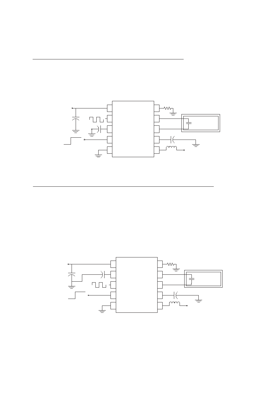
I. Lamp Frequency Control With an External Clock Signal
An external clock signal may be used to control the EL lamp frequency (LF) by applying the clock signal to the CLF pin.
The oscillator frequency can be varied to synchronize the inverter with other elements in the application. An internal
divider network in the IC divides the clock signal by two. The recommended clocking frequencies range from 500Hz
to 1kHz and result in an EL lamp frequency range of 250Hz to 500Hz respectively. The amplitude of the clock signal
typically ranges from 1.0V to V+.
II. Controlling EL Brightness Through Clock Pulse Width Modulation
An external clock signal may be used to control the inductor oscillating frequency (HF). Pulse width modulation of the
external clock signal may be used to regulate the brightness of an EL lamp. In this circuit, when the positive duty cycle
of the external clock is at 20%, the lamp is at full brightness. Incremental dimming occurs as the positive duty cycle is
increased to as high as 85%. This scheme may also be used inversely to regulate lamp brightness over the life of the
battery or to compensate for lamp aging. (Note: Operation at duty cycles higher than 85% and lower than 20% is not
recommended.) The recommended clocking frequency ranges from 10kHz to 24kHz, and the amplitude of the clock
signal typically ranges from 1.0V to V+.
10
V+
CLF
CHF
E
GND
Rd
EL2
EL1
Cs
L+
D372A
1
2
3
4
5
10
9
8
7
6
CHF
0.1
µ
F
Vbat
off
on
EL Lamp
L
Cs
Rd
Vbat
1V
0V
LF CLK
50%DC
V+
CLF
CHF
E
GND
Rd
EL2
EL1
Cs
L+
D372A
1
2
3
4
5
10
9
8
7
6
CLF
0.1
µ
F
Vbat
off
on
EL Lamp
L
Cs
Rd
Vbat
HF CLK
20%-85% +DC
1V
0V
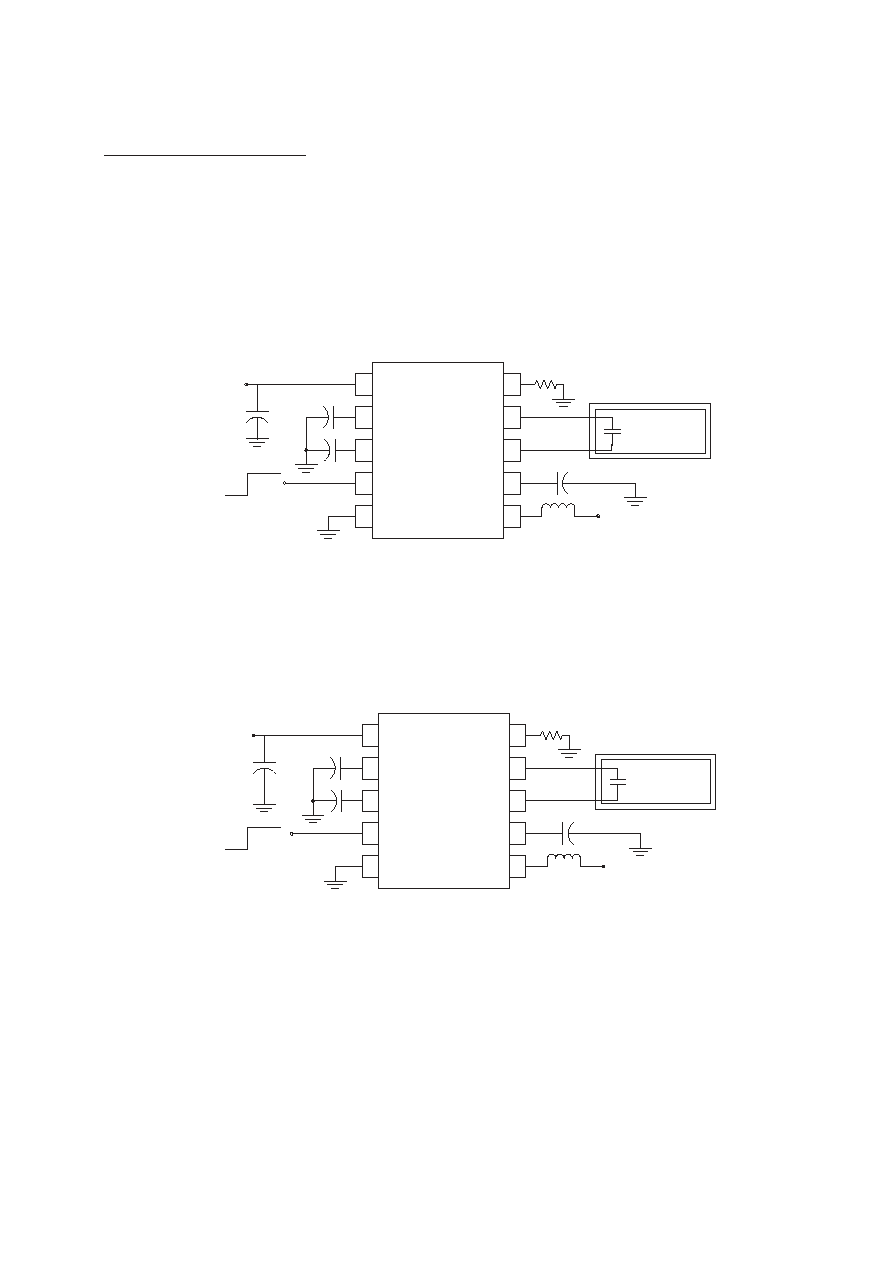
III. Split Voltage Supply
A split supply voltage may also be used to drive the D372. To operate the on-chip logic, a regulated voltage supply (V+)
ranging from 2.0V to 6.5V is applied. To supply the D372 with the necessary power to drive an EL lamp, another supply
voltage (Vbat) is applied to the inductor. The voltage range of Vbat is determined by the following conditions: driver
application, lamp size, inductor selection, and voltage and current limitations.
Two different examples of the split supply are shown below. The first example shows a regulated 3.0V applied to the
V+ pin, and a Vbat voltage that may range from 2.7V to 4.5V. The enable voltage is in the range of 2.0V to 3.0V. This
is a typical setup used in cell phone applications.
The second example shows that V+ may range from 2.0V to 6.5V, and the Vbat voltage may be as high as 12.0V.
The enable voltage is in the range of 2.0V to V+. This is useful in many high voltage applications.
11
V+
CLF
CHF
E
GND
Rd
EL2
EL1
Cs
L+
D372A
1
2
3
4
5
10
9
8
7
6
CHF
0.1
µ
F
V+
Regulated 3.0 V
0 V off
2.0V - 3.0V on
EL Lamp
L
Cs
Rd
Vbat
2.7 V - 4.5 V
CLF
V+
CLF
CHF
E
GND
Rd
EL2
EL1
Cs
L+
D372A
1
2
3
4
5
10
9
8
7
6
CHF
0.1
µ
F
V+
2.0 V - 6.5 V
0V off
2.0V - V+ on
EL Lamp
L
Cs
Rd
Vbat
12.0 V
CLF

DUREL Corporation
2225 W. Chandler Blvd.
Chandler, AZ 85224-6155
Tel: (480) 917-6000
FAX: (480) 917-6049
Website: http://www.durel.com
© 2000, 2001 Durel Corporation
Printed in U.S.A.
LIT-I9032 Rev. A04
The DUREL name and logo are registered trademarks of DUREL CORPORATION.
This information is not intended to and does not create any warranties, express or implied, including any warranty of merchantability or fitness for a
particular purpose. The relative merits of materials for a specific application should be determined by your evaluation.
This driver is covered by the following U.S. patents: #5,313,141, #5,789,870; #6,297,597 B1. Corresponding foreign patents are issued and pending.
ISO 9001 Certified
12
The D372A IC is available in standard MSOP-10 plastic package per tape and reel. A Durel D372 Designer's Kit
(1DDD372AA-K01) provides a vehicle for evaluating and identifying the optimum component values for any particular
application using D372. Durel engineers also provide full support to customers including specialized circuit optimiza-
tion and application retrofits.
Ordering Information
A
0.92
0.036
1.00
0.039
1.08
0.043
B
0.05
0.002
0.10
0.004
0.15
0.006
C
0.15
0.006
0.23
0.009
0.31
0.012
D
0.40
0.016
0.55
0.022
0.70
0.028
E
0.13
0.005
0.18
0.007
0.23
0.009
F
2.90
0.114
3.00
0.118
3.10
0.122
G
0.35
0.014
0.50
0.020
0.65
0.026
H
4.75
0.187
4.90
0.193
5.05
0.199
I
2.90
0.114
3.00
0.118
3.10
0.122
mm.
in.
mm.
in.
mm.
in.
MSOP-10
Min.
Typical
Max.
MSOPs are marked with part number (372A) and 3-digit wafer lot
code. Bottom of marking is on the Pin 1 side.
MSOPs in Tape and Reel:
1DDD372AA-M04
RECOMMENDED PAD LAYOUT
Embossed tape on 360 mm diameter reel per EIA-481-2.
2500 units per reel. Quantity marked on reel label.
Tape Orientation
e
c
a
b
d
f
mm.
in.
mm.
in.
mm.
in.
Min.
Typical
Max.
MSOP-10 PAD LAYOUT
a
0.5
0.0197
b
2.0
0.0788
c
3.3
0.130
3.45
0.136
d
0.89
0.035
0.97
0.038
1.05
0.041
e
5.26
0.207
5.41
0.213
f
0.3
0.012
F
H
I
A
B
G
C
D
E

WWW.ALLDATASHEET.COM
Copyright © Each Manufacturing Company.
All Datasheets cannot be modified without permission.
This datasheet has been download from :
www.AllDataSheet.com
100% Free DataSheet Search Site.
Free Download.
No Register.
Fast Search System.
www.AllDataSheet.com