 | –≠–ª–µ–∫—Ç—Ä–æ–Ω–Ω—ã–π –∫–æ–º–ø–æ–Ω–µ–Ω—Ç: D381A | –°–∫–∞—á–∞—Ç—å:  PDF PDF  ZIP ZIP |
1
General Description:
The Durel
D381A is part of a family of highly integrated EL
drivers based on Durel's patented three-port (3P) topology, which
offers built-in EMI shielding. This high-performance device uses
a proprietary circuit design for programmable wave-shaping for
low-noise performance in applications that are sensitive to audible
and electrical noise.
Data Sheet
D381A
Electroluminescent
Lamp Driver IC
MSOP-8
MSOP-10
∑ Flexible Wave Shaping Capability
∑ Cellular Phones and Handsets
∑ High Efficiency
∑ Data Organizers/PDAs
∑ External Clock Compatible
∑ LCD and Keypad Backlighting
∑ High Voltage AC Output
∑ High Performance with Low-profile Coils
Features
Applications
Standard Test Circuit
uA
E = GND
mA
E = 3.0V
uA
E = 3.0V
Vpp
Hz
CLF=10 nF
kHz
CHF=220 pF
Parameter
Symbol
Minimum
Typical
Maximum
Unit
Conditions
(Using Standard Test Circuit at Ta=25 ∞C unless otherwise specified.)
Lamp Driver Specifications:
Standby Current
0.04
1
Supply Current
I
43
Enable Current
40
50
60
Output Voltage
Vout
158
182
206
Lamp Frequency
LF
230
270
310
Inductor Frequency
HF
17
20
23
D381A
1
2
3
4
5
6
7
8
9
10
CHF
CLF
E
N/C
GND
N/C
L-
Vout
L+
V+
Load B
10 nF
220 pF
D381A
+3.3 V
0.1
µ
F
0.68
mH /
1.7 Ohms DCR
OFF
ON
GND
3.0V
2
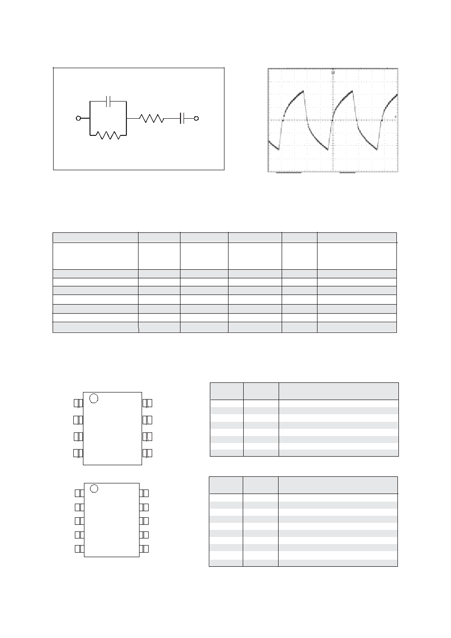
Typical Output Waveform
Load B*
Physical Data:
Absolute Maximum Ratings:
* Load B approximates a 5in
2
EL lamp.
Note: The above are stress ratings only. Functional operation of the device at these ratings or any other above
those indicated in the specifications is not implied. Exposure to absolute maximum rating conditions for extended
periods of time may affect reliability.
Parameter
Symbol
Minimum
Maximum
Unit
Comments
100
22 nF
10k
47 nF
1
2
3
4
5
10
9
8
7
6
1
CHF
High frequency oscillator capacitor/clock input
2
CLF
Lamp frequency capacitor/clock input
3
E
System enable: Wave-shaping resistor control
4
N/C
5
GND
System ground connection
6
N/C
7
L-
Negative input to inductor
8
VOUT
High voltage AC output to lamp
9
L+
Positive input to inductor
10
V+
DC power supply input
PIN # NAME
FUNCTION
PIN # NAME
FUNCTION
1
CHF
High frequency oscillator capacitor/clock input
2
CLF
Lamp frequency capacitor/clock input
3
E
System enable: Wave-shaping resistor control
4
GND
System ground connection
5
L-
Negative input to inductor
6
V
OUT
High voltage AC output to lamp
7
L+
Positive input to inductor
8
V+
DC power supply input
Supply voltage
Operating Range
V+
2.0
7.0
V
E = V+
Withstand Range
-0.4
7.0
E = GND
Enable Voltage
E
-0.4
V+
V
Output Voltage
V
OUT
220
Vpp
Peak-to-peak voltage
CHF Voltage
V
CHF
0
(V+) +0.3 V
External clock input
CLF Voltage
V
CLF
0
(V+) +0.3
V
External clock input
Operating Temperature
T
a
-40
85
∞C
Storage Temperature
T
s
-55
150
∞C
Lamp Resistance
Rlamp
100
1
2
3
4
8
7
6
5
3
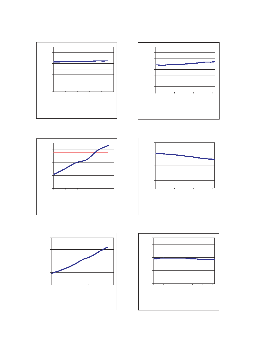
Output Voltage vs. DC Supply Voltage
0
40
80
120
160
200
240
280
2
3
4
5
6
7
DC Input Voltage
Output Voltage (Vpp)
Typical Performance Characteristics
Vout (max)=220Vpp
Output Frequency vs. DC Supply
Voltage
0
50
100
150
200
250
300
350
400
2
3
4
5
6
7
DC Input Voltage
LF (Hz)
Supply Current vs. DC Supply
Voltage
0
10
20
30
40
2
3
4
5
6
7
DC Input Voltage
Avg Supply Current (mA)
Output Frequency vs. Ambient
Temperature
0
50
100
150
200
250
300
350
400
-40
-20
0
20
40
60
80
Temperature ( C)
LF (Hz)
∞∞
∞∞
∞
Output Voltage vs. Ambient
Temperature
0
40
80
120
160
200
240
-40
-20
0
20
40
60
80
Temperature ( C)
Output Voltage (Vpp)
Supply Current vs. Ambient
Temperature
0
10
20
30
40
50
60
70
-40
-20
0
20
40
60
80
Temperature ( C)
Avg Supply Current (mA)
∞∞
∞∞
∞
∞∞
∞∞
∞
4
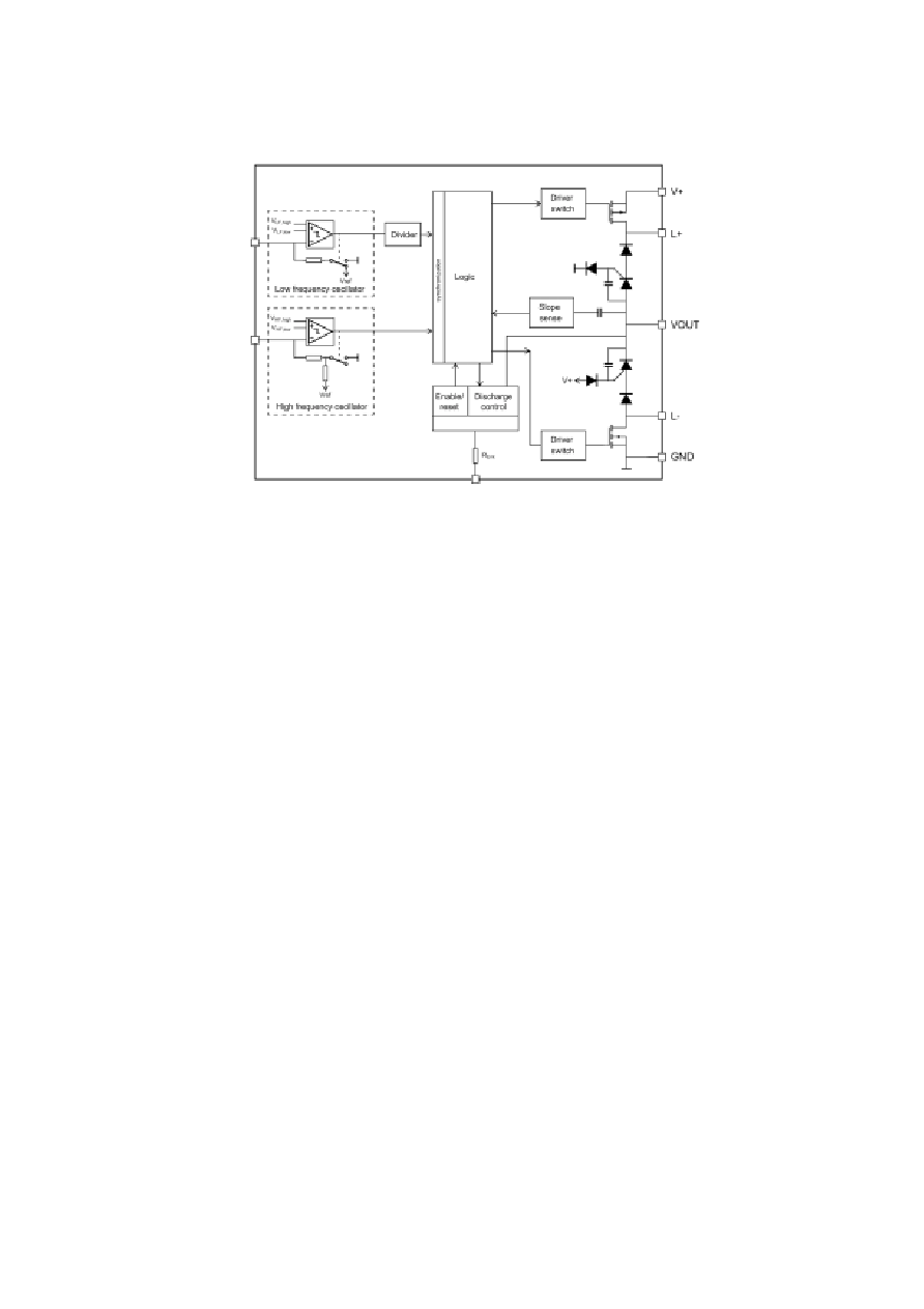
Theory of Operation
Electroluminescent (EL) lamps are essentially capacitors with one transparent electrode and a special phosphor material
in the dielectric. When a strong AC voltage is applied across the EL lamp electrodes, the phosphor glows. The
required AC voltage is typically not present in most systems and must be generated from a low voltage DC source.
Thus, Durel developed its patented Three-Port (3P) switch-mode inverter circuit to convert the available DC supply
to an optimal drive signal for high brightness and low-noise EL lamp applications. The Durel 3P topology offers the
simplicity of a single DC input, single AC output, and a shared common ground that provides an integrated EMI
shielding.
The D381A drives the EL lamp by repeatedly pumping charge through an external inductor with current from a DC
source and discharging into the capacitance of the EL lamp load. With each high frequency (HF) cycle the voltage on
the lamp is increased. At a period specified by the lamp frequency (LF) oscillator, the voltage on the lamp is discharged
to ground and the polarity of the inductive charging is reversed. By this means, an alternating positive and negative
voltage is developed at the single output lead of the device to one of the electrodes of the EL lamp. The other lamp
electrode is commonly connected to a ground plane, which can then be considered as electrical shielding for any
underlying circuitry on the application.
The EL driving system is divided into several parts: on-chip logic and control, on-chip high voltage output circuitry,
discharge logic circuitry, and off-chip components. The on-chip logic controls the output frequency (LF), as well as the
inductor switching frequency (HF), and HF and LF duty cycles. These signals are combined and buffered to regulate
the high voltage output circuitry. The output circuitry handles the power through the inductor and delivers the high
voltage to the lamp. The selection of off-chip components provides a degree of flexibility to accommodate various lamp
sizes, system voltages, and brightness levels. Since a key objective for EL driver systems is to save space and cost,
required off-chip components were kept to a minimum.
Durel provides a D381A Designer's Kit, which includes a printed circuit evaluation board intended to aid you in
developing an EL lamp driver configuration using the D381A that meets your requirements. A section on designing
with the D381A is included in this datasheet to serve as a guide to help you select the appropriate external components
to complete your D381A EL driver system.
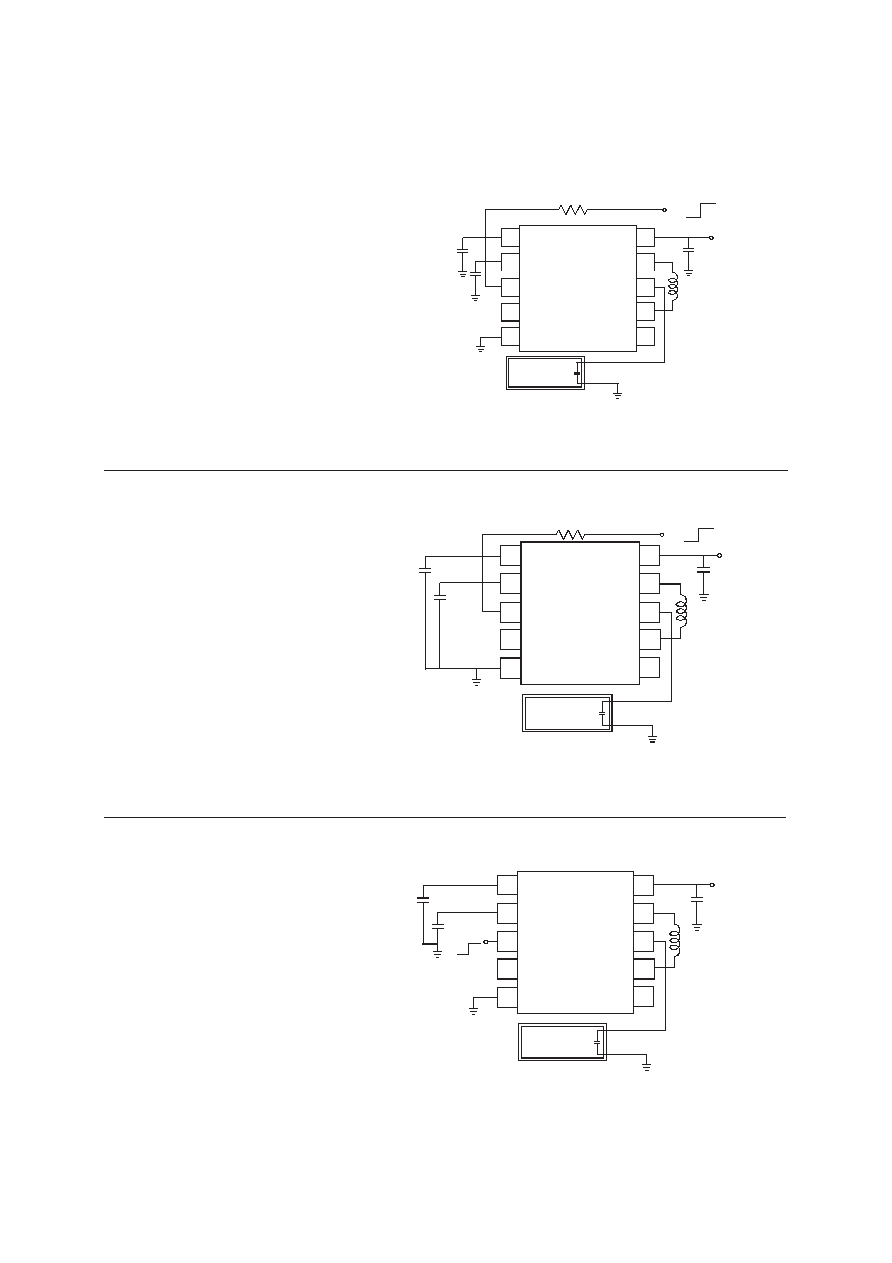
Typical D381A configurations for driving EL lamps in various applications are shown on the following page. The
expected system outputs, such as lamp luminance, lamp output frequency and voltage and average supply current
draw, for the various sample configurations are also shown with each respective figure.
Block Diagram of the Driver Circuitry
CLF
CHF
E
5
Typical D381A EL Driver Configurations
3.0V Handset LCD
Typical Output
Luminance= 9.7 fL (33.2 cd/m
2
)
Lamp Frequency = 392 Hz
Supply Current = 15 mA
Vout = 210 Vpp
Load = 1.5 in
2
(950 mm
2
)Durel Green EL
5.0V PDA
Typical Output
Luminance = 7.1 fL (24.35 cd/m
2
)
Lamp Frequency = 280 Hz
Supply Current = 18 mA
Vout = 211 Vpp
Load = 4 in
2
(2580 mm
2
) Durel Green EL
3.3V Handset LCD and Keypad
Typical Output
Luminance = 6.9 fL (23.6 cd/m
2
)
Lamp Frequency = 266 Hz
Supply Current = 13 mA
Vout = 200 Vpp
Load = 2.25in
2
(1550 mm
2
) Durel Green EL
1
2
3
4
5
6
7
8
9
10
CHF
CLF
E
N/C
GND
N/C
L-
Vout
L+
V+
1.5 in
2
EL Lamp
6.8 nF
.68mH Murata LQH4N
68 pF
D381A
3.0V
1.0
µ
F
82k
OFF
ON
GND
3.0V
1
2
3
4
5
6
7
8
9
10
CHF
CLF
E
N/C
GND
N/C
L-
Vout
L+
V+
2.25 in
2
EL Lamp
10 nF
1mH Sumida CLS62
68 pF
D381A
1.0 u F
82k
OFF
ON
GND
3.0V
1
2
3
4
5
6
7
8
9
10
CHF
CLF
E
N/C
GND
N/C
L-
Vout
L+
V+
4 in
2
EL Lamp
1.0 nF
Bujeon BDS4020S
1.5 mH
68 pF
D381A
+5.0 V
1.0 u F
OFF
ON
GND
5.0V
6
Designing With D381A
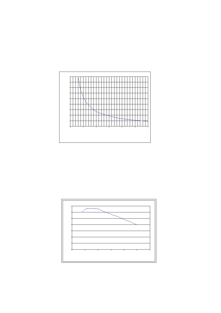
I. Lamp Frequency Capacitor (CLF) Selection
Selecting the appropriate value of lamp frequency capacitor (CLF) for the low frequency oscillator will specify the
output frequency of the D381A EL driver. Lamp frequencies of 200-500 Hz are typically used. Figure 1 graphically
represents the inversely proportional relationship between the CLF capacitor value and the oscillator frequency.
Alternatively, the lamp frequency may also be controlled with an external clock signal. There is an internal frequency
divider in the device so that the output lamp frequency will be half of the input clock signal. For example, if a 500Hz
input clock signal is used, the resulting lamp frequency will be 250Hz. The clock signal input voltage should not exceed
V+.
The selection of the CLF value can also affect the brightness of the EL lamp because of its control of the lamp frequency
(LF). Although input voltage and lamp size can change EL lamp frequency as well, LF mainly depends on the CLF
value selected or the frequency of the input clock signal to CLF. Figure 2 shows typical brightness of a D381A circuit
with respect to lamp frequency. In this example, the inductor and CHF values were kept constant while varying LF.
Figure 1: Typical Lamp Frequency vs. CLF Capacitor
Figure 2: Luminance vs. Lamp Frequency
(V+=3.0V, 2.4in
2
Durel 3 Green EL Lamp Load)
0
100
200
300
400
500
600
700
800
900
0
5
10
15
20
25
30
CLF (nF)
Lamp Frequency (Hz)
0
1
2
3
4
5
6
7
0
200
400
600
800
1000
1200
Lamp Frequency (Hz)
Lamp Luminance (fL)
7
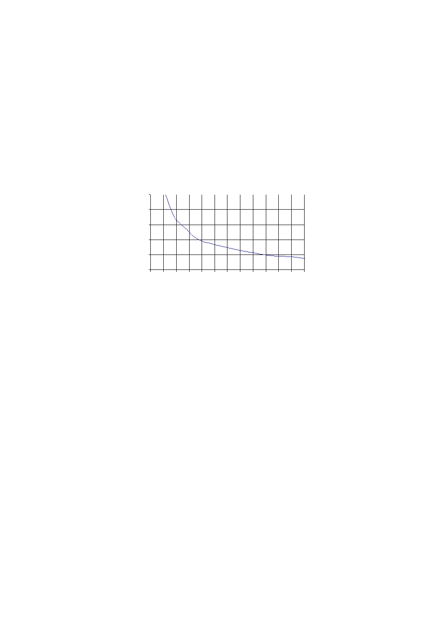
II. High Frequency Capacitor (CHF) Selection
Selecting the appropriate value of capacitor for the high frequency oscillator (CHF) will set the inductor switching
frequency of the D381A IC. High inductor frequency allows for more efficient use of inductor coils with lower values.
However, care must be taken that the charge pumping does not reach a continuous mode at very high frequency when
the voltage is not efficiently transferred to the lamp load. Figure 3 graphically represents the effect of the CHF value
on the oscillator frequency at V+=3.0V.
Figure 3: Typical InductorFrequency vs. CHF Capacitor
The inductor switching frequency may also be controlled with an external clock signal. The inductor will charge during
the low portion of the clock signal and discharge into the EL lamp during the high portion of the clock signal. The
positive duty cycle used for the external high frequency clock signal is usually between 15%-75%, with a typical value
of 15%-20% for maximum brightness. The clock signal input voltage should not exceed V+.
0
20
40
60
80
100
120
0
25
50
75 100 125 150 175 200 225 250 275 300
CHF (pF)
Inductor Frequency (kHz)
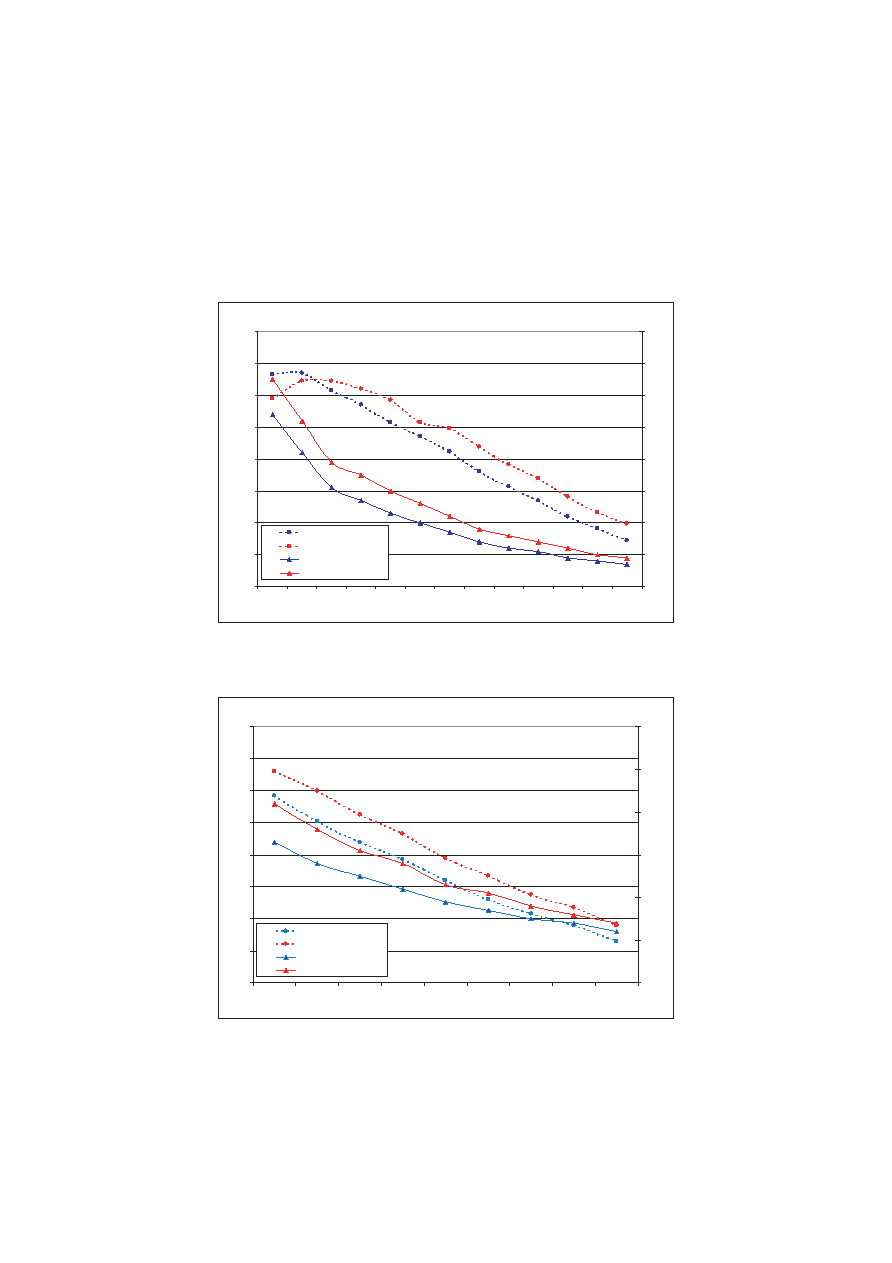
The inductor value and inductor switching frequency have the greatest impact on the output brightness and current
consumption of the EL driver. Figures 4 and 5 show the dependence of brightness and current draw of a D381A circuit
on coil values and CHF values for two sample EL lamps sizes and input voltages. The CLF value was chosen such that
the output voltage did not exceed 220Vpp. Please note that the DC resistance (DCR) of inductors with the same nominal
inductance value may vary with manufacturer and inductor type. Thus, inductors made by a different manufacturer
may yield different outputs, but the trend of the different curves should be similar.
III. Inductor (L) Selection
Figure 4: Brightness and current vs. inductor and CHF value
(Conditions: V+=3.0V, 2in
2
EL Lamp)
Figure 5: Brightness and current vs. inductor and CHF value
(Conditions: V+=5.0V, 4in
2
EL Lamp)
0
2
4
6
8
10
12
14
16
0.15
0.22
0.33
0.39
0.47
0.56
0.68
0.82
1.00
1.20
1.50
1.80
2.20
Inductor (mH)
0
10
20
30
40
50
60
70
80
68 pF Brightness
100 pF Brightness
68 pF Current
100 pF Current
Brightness (ftL)
Current (mA)
0
2
4
6
8
10
12
14
16
0.68
0.82
1
1.2
1.5
1.8
2.2
2.7
3.3
Inductor (mH)
0
10
20
30
40
50
60
68 pF Brightness
100 pF Brightness
68 pF Current
100 pF Current
Brightness (ftL)
Current (mA)
8
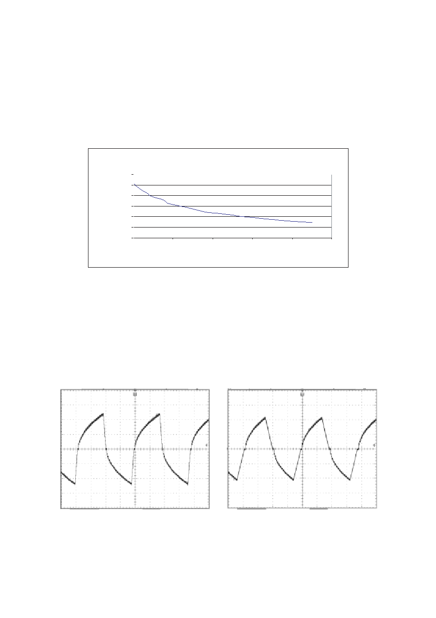
IV. Wave-Shape Selection
The D381A driver IC uses a patented wave-shaping technique for reducing audible noise from an EL lamp. The linear
discharge of the output waveform may be adjusted by selecting a proper value for the wave-shaping resistor (Rena) to
the E pin. The optimal discharge level for an application depends on the lamp size, lamp brightness, and application
conditions. To ensure that the D381A is configured optimally, various discharge levels should be evaluated. In many
cases, the lower discharge levels result in lower audible noise from the EL lamp.
9
Typical waveshapes corresponding to the various discharge levels for a 4in
2
lamp are shown below. The waveshape
with the smoothest transition slope in the discharge portion of the waveform yields the lowest audible noise.
R
ena
=0
R
ena
=82k
Figure 6: R
ena
selection for discharge control (C
LOAD
=15nF), (E= 3V)
D381 Discharge Control
0.00
2.00
4.00
6.00
8.00
10.00
12.00
0.0
20.0
40.0
60.0
80.0
100.0
Rena (KOhm)
ldischarge (mA)
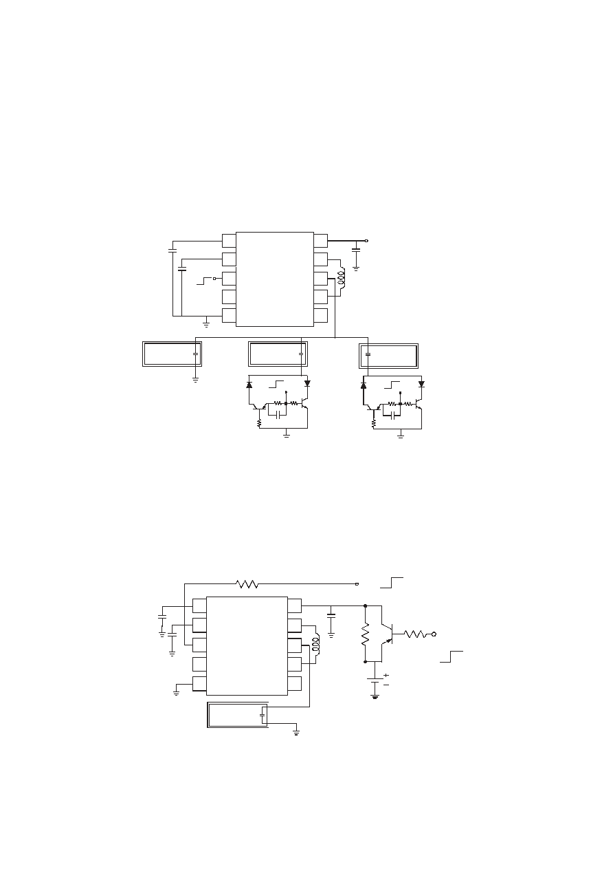
D381A Design Ideas
I. Driving Multi-segment Lamps
The D381A may be used to drive multiple EL lamp segments. An external transistor switching circuit is used to turn
each lamp segment on or off independently or simultaneously. A high signal at the corresponding E input will enable
the corresponding lamp segment. In this configuration, EL Lamp 1 is always turned on when the IC is enabled.
Otherwise, always make sure that at least one segment is selected when the D381A is enabled.
10
II. Two-Level Dimming
Two level dimming may be achieved with the circuit below. When DIM is low, the external PNP transistor is saturated
and the EL lamp runs at full brightness. When DIM is high, the external PNP turns off and the 47
resistor reduces the
voltage at (V+) and dims the EL lamp.
OFF
ON
V
bat
R
switch
1k
DIM
2N3906
1
2
3
4
5
6
7
8
9
10
CHF
CLF
E
N/C
GND
N/C
L-
Vout
L+
V+
EL
Lamp
CLF
L
CHF
D381A
V
ENA
1.0 u F
R
enable
BRIGHT
DIM
3V
0V
1
2
3
4
5
6
7
8
9
10
CHF
CLF
E1
N/C
GND
N/C
L-
Vout
L+
V+
D381A
Vbat
0.1 u F
OFF
ON
EL Lamp 2
EL Lamp 3
E2
2.2K
4.7K
BAS21LT1
BAS21LT1
MMBT5401LT1
MMBT5551LT1
1K
E3
2.2K
4.7K
BAS21LT1
BAS21LT1
MMBT5401LT1
MMBT5551LT1
1K
EL Lamp 1
100 nF
100 nF
OFF
ON
OFF
ON
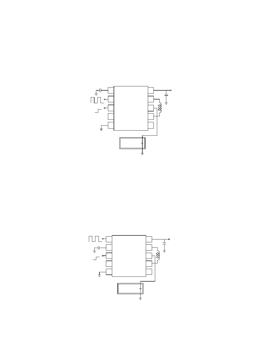
III. Lamp Frequency Control with an External Clock Signal
An external clock signal may be used to control the EL lamp frequency (LF) of the D381A instead of using a capacitor.
There is an internal frequency divider in the IC so that the output lamp frequency will be half of the input clock signal.
For example, if a 500Hz input clock signal is used, the resulting lamp frequency will be 250Hz. The clock signal voltage
should not exceed V+. A typical duty cycle for the clock input is +50%.
IV. EL Brightness through HF Clock Pulse Width Modulation
The inductor oscillating frequency may also be controlled on the D381A EL driver IC using an external clock input to
CHF. In addition, pulse-width modulation of the external HF clock signal to the D381A may be used to regulate the
brightness of the EL lamp load. High frequency input is typically in the range of 10kHz to 40kHz, with duty cycle in the
range of 15% to 100%. In general, a lower HF frequency results in higher brightness and using a lower duty cycle
results in higher brightness. The clock signal voltage should not exceed V+. Prior to finalization of the circuit, contact
Durel to verify that the frequency, duty cycle, and setup chosen are acceptable for EL driver performance.
11
1
2
3
4
5
6
7
8
9
10
CHF
CLF
E
N/C
GND
N/C
L-
Vout
L+
V+
D381A
Vbat
0.1 u F
OFF
ON
EL Lamp
1.0V Min
0.2V Max
10KHz - 40KHz
15%-75% Duty
1
2
3
4
5
6
7
8
9
10
CHF
CLF
E
N/C
GND
N/C
L-
Vout
L+
V+
D381A
Vbat
0.1 uF
OFF
ON
EL Lamp
1.0V Min
0.2V Max
200Hz - 2KHz
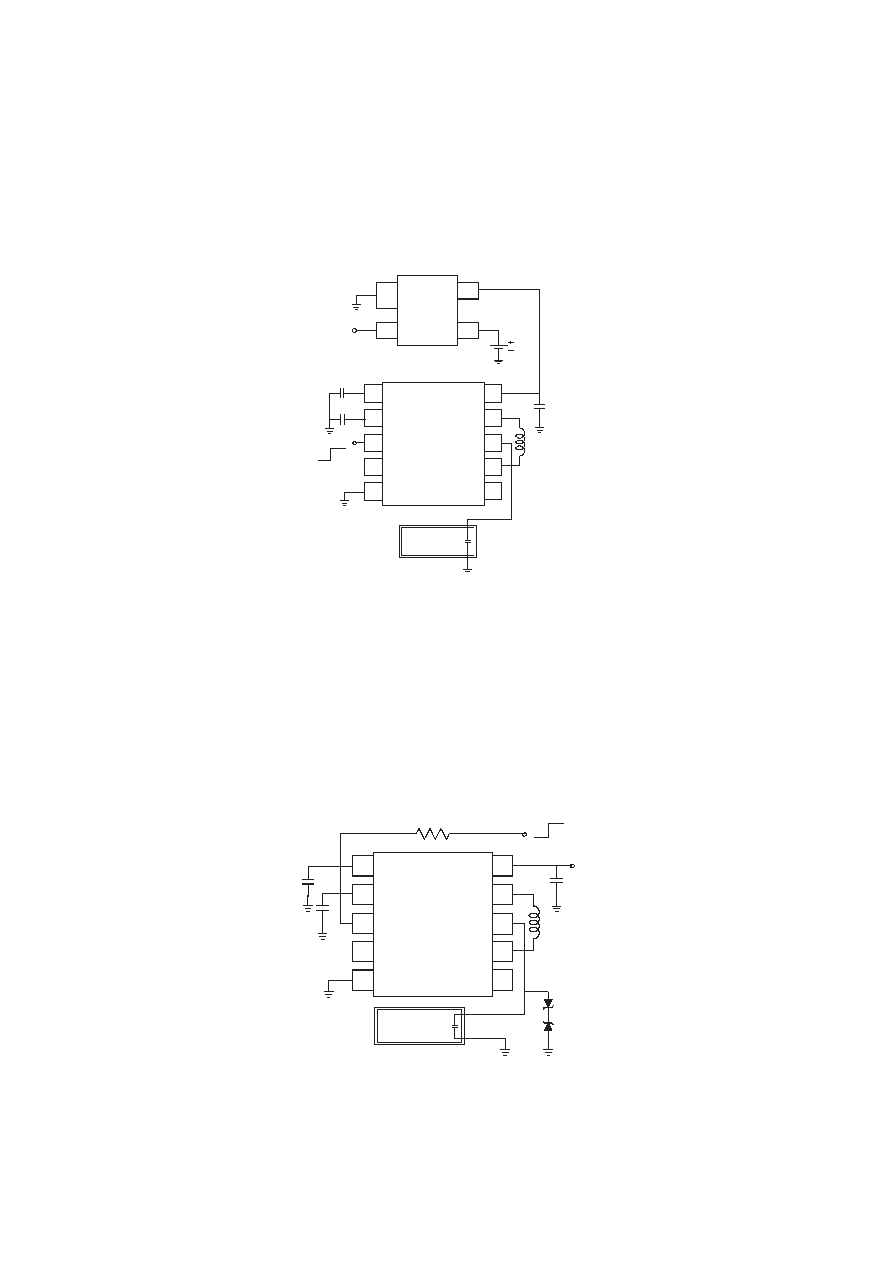
V. EL Lamp Brightness Regulation
Regulating the DC supply input voltage to the D381A will result in a constant brightness level from the EL lamp,
regardless of battery voltage. In this example, a Micrel voltage regulator is used.
12
VI. Output Voltage Limit Control
An EL driver system using the D381A driver IC should be designed such that the output voltage does not exceed the
maximum rated value of 220Vpp. A pair of zener diodes connected to the output as shown below is recommended to
limit Vout to within 200Vpp or less. This circuit protects the device from over-voltage when typical performance is near
the maximum limit for the D381A.
1
2
3
4
5
6
7
8
9
10
CHF
CLF
E
N/C
GND
N/C
L-
Vout
L+
V+
EL
Lamp
CLF
L
CHF
D381A
V
BAT
1.0 uF
R
enable
1N5271 or
equivalent
100V zener
diodes
OFF
ON
1
2
3
4
5
6
7
8
9
10
CHF
CLF
E
N/C
GND
N/C
L-
Vout
L+
V+
D381A
0.1 uF
OFF
ON
EL Lamp
Vbat
1 GND
2 E
OUT
IN
4
3
MIC5203
E
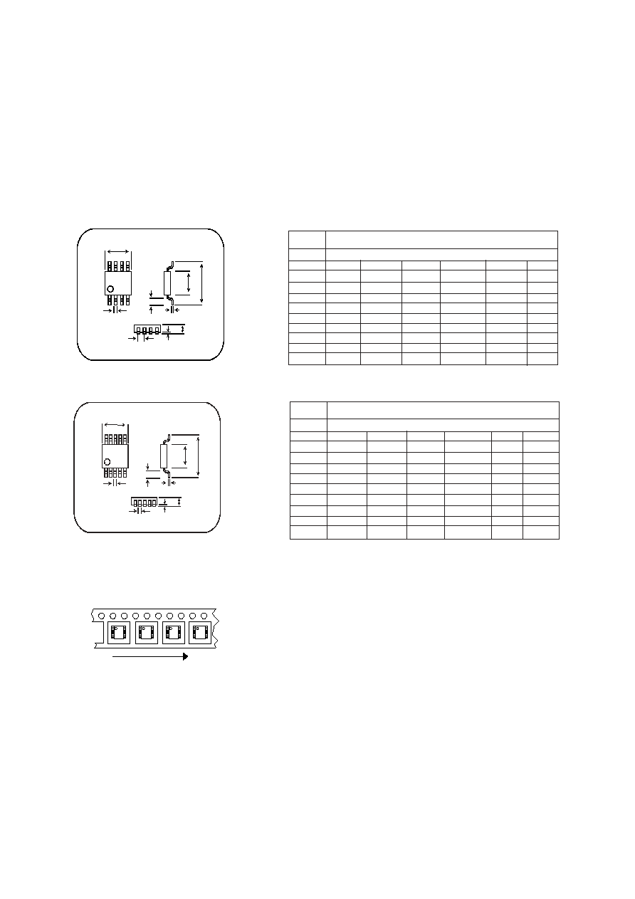
The D381A IC is available in standard MSOP-8 or MSOP-10 plastic package tape and reel. A Durel D381A Designer's
Kit (1DDD381AA-K01) provides a vehicle for evaluating and identifying the optimum component values for any
particular application using D381A. Durel engineers also provide full support to customers, including specialized
circuit optimization and application retrofits.
Ordering Information
MSOPs in Tape and Reel:
MSOP-8: 1DDD381AA-M02
MSOP-10: 1DDD381AA-M04
Tape Orientation
Embossed tape on 360 mm diameter per reel.
2500 units per reel.
13
A
0.92
0.036
1.00
0.039
1.08
0.043
B
0.05
0.002
0.10
0.004
0.15
0.006
C
0.15
0.006
0.23
0.009
0.31
0.012
D
0.40
0.016
0.55
0.022
0.70
0.028
E
0.13
0.005
0.18
0.007
0.23
0.009
F
2.90
0.114
3.00
0.118
3.10
0.122
G
0.35
0.014
0.50
0.020
0.65
0.026
H
4.75
0.187
4.90
0.193
5.05
0.199
I
2.90
0.114
3.00
0.118
3.10
0.122
MSOPs are marked with part number (381A), 5-digit wafer lot code and a 3-digit date
code. Bottom of marking is on the Pin 1 side.
F
H
I
A
B
G
C
D
E
A
0.94
0.037
1.02
0.040
1.09
0.043
B
0.05
0.002
0.10
0.004
0.15
0.006
C
0.20
0.008
0.33
0.013
0.46
0.018
D
0.41
0.016
0.53
0.021
0.65
0.026
E
0.13
0.005
0.18
0.007
0.23
0.009
F
2.84
0.112
3.00
0.118
3.15
0.124
G
0.43
0.017
0.65
0.026
0.83
0.033
H
4.70
0.185
4.90
0.193
5.11
0.201
I
2.84
0.112
3.00
0.118
3.25
0.128
Description
mm.
in.
mm.
in.
mm.
in.
MSOP-8
Min.
Typical
Max.
mm.
in.
mm.
in.
mm.
in.
MSOP-10
Min.
Typical
Max.
MSOPs are marked with part number (381A), 5-digit wafer lot code and a 3-digit date
code. Bottom of marking is on the Pin 1 side.
F
H
I
A
B
G
C
D
E
14
The DUREL name and logo are registered trademarks of DUREL CORPORATION.
This information is not intended to and does not create any warranties, express or implied, including any warranty of merchantability or fitness for a
particular purpose. The relative merits of materials for a specific application should be determined by your evaluation.
This driver is covered by the following U.S. patents: #5,313,141, #5,347,198; #5,789,870 #6,043,610. Corresponding foreign patents are issued and pending.
DUREL Corporation
2225 W. Chandler Blvd.
Chandler, AZ 85224-6155
Tel: (480) 917-6000
FAX: (480) 917-6049
Website: http://www.durel.com
© 2001, 2002 Durel Corporation
Printed in U.S.A.
LIT-I 9040 Rev. A03
ISO 9001 Certified
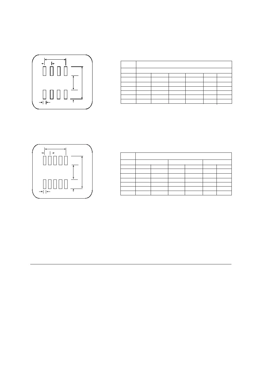
RECOMMENDED PAD LAYOUT
e
c
a
b
d
f
mm.
in.
mm.
in.
mm.
in.
Min.
Typical
Max.
a
0.60
0.0236
0.6
0.0256
0.70
0.0276
b
1.90
0.0748
1.9
0.0768
2.00
0.0788
c
3.3
0.130
3.45
0.136
d
0.89
0.035
0.9
0.038
1.05
0.041
e
5.26
0.207
5.41
0.213
f
0.41
0.016
0.4
0.018
0.51
0.020
MSOP-8 PAD LAYOUT
e
c
a
b
d
f
mm.
in.
mm.
in.
mm.
in.
Min.
Typical
Max.
MSOP-10 PAD LAYOUT
a
0.5
0.0197
b
2.0
0.0788
c
3.3
0.130
3.45
0.136
d
0.89
0.035
0.97
0.038
1.05
0.041
e
5.26
0.207
5.41
0.213
f
0.3
0.012
WWW.ALLDATASHEET.COM
Copyright © Each Manufacturing Company.
All Datasheets cannot be modified without permission.
This datasheet has been download from :
www.AllDataSheet.com
100% Free DataSheet Search Site.
Free Download.
No Register.
Fast Search System.
www.AllDataSheet.com