 | –≠–ª–µ–∫—Ç—Ä–æ–Ω–Ω—ã–π –∫–æ–º–ø–æ–Ω–µ–Ω—Ç: D6002 | –°–∫–∞—á–∞—Ç—å:  PDF PDF  ZIP ZIP |
S
ilicore
SHAOXING SILICORE TECHNOLOGY CO.,LTD
www. Silicore. com. cn
CHMC
1/6
RADIO CONTROLLED RECEIVER IC D6002
DESCRIPTION
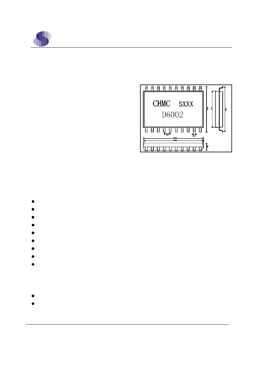
Out li ne Dra wi ng
The D6002 i s a bi pola r integrate d straight
through rec eiver c ircuit in the frequency range
from 40kHz up t o 200kHz wit h ASK modula tion.
The IC rece ivers and demodul at es ti me code
signals transmi tt ed by DCF77,M SF , WWVB
and G2AS.
The devi ces is designed for radi o c ontrolle d
cl oc k a ppli cat ions wi th very hi gh sensi tivi ty.
Int egrated funct ions as s tand by mode and
compl ementa ry out put st age s offer fe atures for
uni ve rsa l appli cat ions.
The BIP2 te chnology makes al l the above feat ures possible for ve ry l ow cost
applic ati ons.
FEATURE
Single chi p strai ght through rece ive r.
Low power ba tt ery a ppli cati ons(1. 1~ 3.6V)
Very low power c onsumpti on.
Powe r down modus.
Wi de fre quency range (40~ 200kHz )
Very high se nsi ti vi ty.
High sel ecti vi ty by qua rt z re sonator.
Comple menta ry output sta ge s.
M inimum exte rnal compone nt s.
APPLICATIONS
Re cei ve r for t ime c ode t rans mit te r signal's
Re cei ver for ASK modul ate d dat e si gnal 's.
Silicore
D6002
SHAOXING SILICORE TECHNOLOGY CO.,LTD
www. Silicore. com. cn
CHMC
2/6
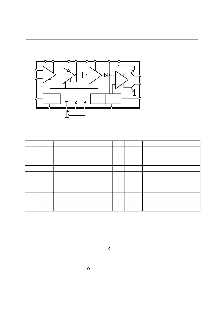
BLOCK DIAGRAM
+
-
Peak
Detector
Gain
Control
RF Amp
Post Amp
Bias
Comparator
O1
O2
IC
CD1 CD2
IA1
IA2
VDD
Vcc
GND1
GND2
GND3
CAGC
CDEM
CD3
OD1
OD2
PON
STOP
(Post Amp)
(RF Amp)
PIN DEFINITION
Pin Symbol
Desc ri pti on
Pin
Symbol
Desc ri ption
1
GND2
Ground 2 (R F sta ge s).
11
PON
Power on
2
C D1
Decoupli ng ca pa cit or C 1
12
STOP
AGC st op
3
C D2
Decoupli ng c apacit or C 1
13
C AGC
AGC ca pa cit or
4
IA1
Antenna i nput 1
14
C DE M
Demodulat ion capaci tor
5
Vcc
Supply vol tage
15
GND3
Ground 3(Post ampli fier)
6
IA2
Antenna i nput 2
16
NC
Not c onne cte d
7
V
D D
Supply vol tage for
compa ra tor and output st age
17
CD3
Dec oupl ing capaci tor C2
8
OD1
Data out put 1 (pul l down)
18
IC
C ryst al input
9
OD2
Dat a out put 2 (pul l up)
19
O2
Non-inverting RF output
10
GND1
Ground 1(output sta ge s)
20
O1
Invert ing RF output
PON Power on/ off c ontrol
If PON is connect ed to GND/ Vc c t he D6002 rece iver is acti ve/st and-by.
OD1 Da ta output 1
The output si gnal can dire ctl y dec oded by a mic roproce ssor.
The output OD1 i s a PNP ope n coll ect or stage wi th hi gh ac tive l ogi c. The
connec tion wi th a n ext erna l re sist or of 100k t o GND i s possibl e.
OD2 Da ta output 2
The output OD2 is a NPN open coll ect or stage wit h low ac ti ve logic. The connect ion
wit h an external re sist or of 100k t o Vcc is possible.

Silicore
D6002
SHAOXING SILICORE TECHNOLOGY CO.,LTD
www. Silicore. com. cn
CHMC
3/6
GND1 Ground 1
GND1 i s the c ontrol ground pote ntia l for the complet e ci rcui t. GND1 have to
connec ted t o GND2/ GND3.
GND2 Ground 2
The Pin GND2 i s t he ground potenti al for t he RF ampl ifi er and ha s t o connec ted t o
GND1.
GND3 Ground 3
The Pin GND3 is the ground potent ial for the Post ampl ifie r and has to connec ted
to GND1.
STOP AGC stop
If STOP is c onne cte d t o GND/ Vcc the AGC c ircuit is off/on
CAGC AGC capaci tor
The Pi n CAGC i s connect ed to an exte rnal capaci tor aga inst GND. It i s ne cessary
t o generat e the pea k val ue of t he de modul ator output vol ta ge signal . The pe ak val ue
cont rol s the AGC.
CDEM Demodulat ion capaci tor
The Pin CDEM i s c onne cte d to an exte rnal c apaci tor agai nst GND. It is necessary
for t he demodulat ion of the AM signal.
CD3 Decoupli ng c apac it or C2
The Pin CD3 is conne cte d t o an e xt erna l ca pac it or agai nst GND. It is nec essary for
the st abil ity of the post ampl ifie r. The values of t he e xt erna l capac itor i nfl ue nc e t he
fre quency response of the post ampl ifie r.
ABSOLUTE MAXIMUM RATINGS
(Ta =25 C)
Chara cte ri sti c
Symbol
M in
Ma x
Uni t
Supply Vol tage Vcc
Vcc
0
5.5
V
Supply Vol tage V
D D
V
D D
0
5.5
V
Out put Volt age OD1
V
O D 1
-0.3
V
D D
+ 0.3
V
Out put Volt age OD2
V
O D 2
-0.3
V
D D
+ 0.3
V
Swit ch Volt age STOP
V
S T O P
-0.3
V
D D
+ 0.3
V
Swit ch Volt age PON
V
P O N
-0. 3
V
D D
+ 0.3
V
Junc tion Te mperat ure
Tj
-55
150
C
St orage Tempe rature R ange
Tst g
-55
150
C
El ect rost ati c handl ing (M IL s tanda rd 863C )
ESD
-2000
+ 2000
V

Silicore
D6002
SHAOXING SILICORE TECHNOLOGY CO.,LTD
www. Silicore. com. cn
CHMC
4/6
ELECTRICAL CHARACTERISTICS
(They apply wit hin the spec ifie d ope rati ng condit ions unle ss otherwise speci fi ed.)
Chara cte ri sti cs
Symbol
Test c ondi tions
M in Typ Ma x
Uni t
Out put pulse Durati on(OD1,OD2)
t
W O D k
170
195
230
ms
Input Vol tage(IC)
V
I N I C
30
300
Vrms
Input R esist anc e(IA1,IA2)
R
I N
600
k
Input R esist anc e(IC )
R
I N
400
k
Input R esi st ance De modul ator
R
I N
50
k
RF-gai n
G
R F m a x
V
C A G C
=0V
56
dB
RF ga in
G
R F m i n
V
C A G C
=Vcc
-40
dB
Out put Volt age Demodula tor
V
O U T D E M
0.25
Vp-p
TEST CIRCUIT
+
-
Peak
Detector
Gain
Control
RF Amp
Post Amp
Bias
Comparator
O1
O2
IC
CD1
CD2
IA1
IA2
VDD
Vcc
GND1
GND2
GND3
CAGC
CDEM
CD3
OD1
OD2
PON
STOP
(Post Amp)
(RF Amp)
C4
4.7uF
C3
C2
C1
6.8nF
Q1
VDD
Vcc
Tr
1M

Silicore
D6002
SHAOXING SILICORE TECHNOLOGY CO.,LTD
www. Silicore. com. cn
CHMC
5/6
TYPICAL APPLICATION CIRCUIT
O1
O2
IC
CD1
CD2
IA1
IA2
VDD
Vcc
GND1
GND2
GND3
CAGC
CDEM
CD3
OD1
OD2
PON
STOP
6.8nF
1.8nF~6.8nF
VDD=3V
Antenna L1
f =77.5kHz
R EG
4.7uF
22nF
47nF
VDD
µc
D
6
0
0
2
APPLICATION CIRCUIT for WWVB 60kHz
O1
O2
IC
CD1
CD2
IA1
IA2
VDD
Vc c
GND1
GND2
GND3
CAGC
CDEM
CD3
OD1
OD2
PON
STOP
6.8nF
1.8nF~6.8nF
VDD=3V
Antenna L1
f =60kHz
R EG
4.7uF
22nF
47nF
VDD
µc
D
6
0
0
2

Silicore
D6002
SHAOXING SILICORE TECHNOLOGY CO.,LTD
www. Silicore. com. cn
CHMC
6/6
APPLICATION CIRCUIT for MSF 50kHz
O1
O2
IC
CD1
CD2
IA1
IA2
VDD
Vcc
GND1
GND2
GND3
CAGC
CDEM
CD3
OD1
OD2
PON
STOP
6.8nF
1.8nF~6.8nF
VDD=3V
Antenna L1
f =50kHz
R EG
4.7uF
22nF
47nF
VDD
µc
D
6
0
0
2
APPLICATION HINT'S
The PC B has to be desi gned for RF condit ions.
The fe rrit e a nt enna is a crit ica l devi ce s of t he c ompl et e c lock recei ve r.
The di me nsi oning of the antenna resonant resi sta nce is a compromi se be twee n hi gh
si gnal vol tage and low antenna noi se volt age . The Q-fac tor of antenna should be hi gh
for a tt enuat ion of infe rence signal's. In t he appl ic ati on circui t i s t he Rref 100k,
Q=80.
To achieve a hi gh sel ect ivit y the parasit ic paral lel capacit ance of the crysta l should be
1~1.5pF.
For a t roubl e-free re cepti on the ca pac it or on GND and CD3 have t o be arranged nearby
the chi p foot prints.