 | ÐлекÑÑоннÑй компоненÑ: DM134B | СкаÑаÑÑ:  PDF PDF  ZIP ZIP |
Äîêóìåíòàöèÿ è îïèñàíèÿ www.docs.chipfind.ru

DM134B
DM135B
Version :
A.001
Issue Date :
2004/4/29
File Name
:
SP-DM134B,135B-A.001.doc
Total Pages:
18
16-Bit Constant Current LED Drivers with
3.3v ~ 5v Supply Voltage
9
9
9
9
7
7
7
7
1
1
1
1
SILICON TOUCH TECHNOLOGY INC.
9-7F-1, Prosperity Road I, Science Based Industrial Park,
Hsin-Chu, Taiwan 300, R.O.C.
Tel886-3-5645656 Fax886-3-5645626

DM134B
DM135B
SILICON TOUCH TECHNOLOGY INC.
16-Bit Constant Current LED Drivers
-
1-
Version
A.001
Preliminary
DM134B
DM135B
16-Bit Constant Current LED Drivers with
3.3v ~ 5v Supply Voltage
General Description
The DM134BDM135B are constant current drivers specifically designed for LED display
applications. The value of constant current can be varied using an external resistor. The devices
include a 16-bit shift register, latches, and constant current drivers on a single Silicon CMOS
chip.
Features
3.3V~5V CMOS Compatible Input
Maximum Clock Frequency: 25MHz (Cascade Operation)
Maximum Output Voltage: 17V
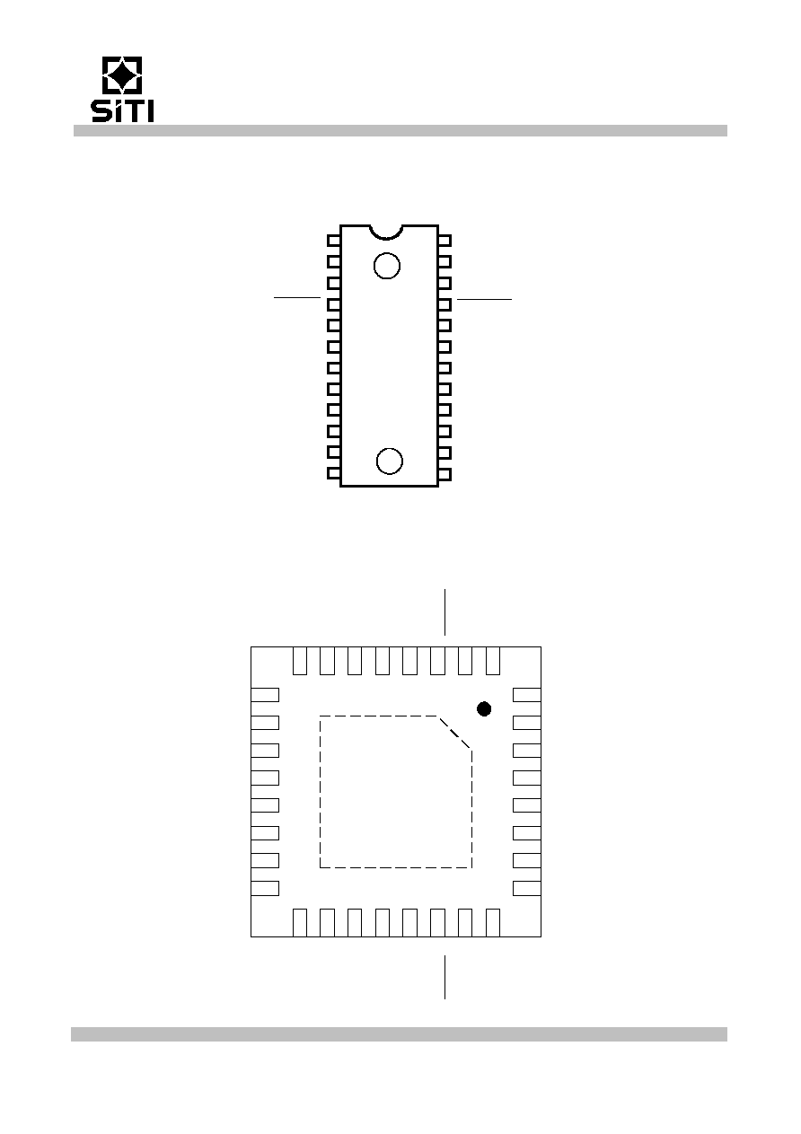
Package:
DIP24,
SOP24,
SSOP24,
QFN32
Package and Pin Layout:
Pin layout and functionality are similar to those of the ST2221C.
(Each characteristic value is different.)
Constant Current Matching: (Ta = 25
°
CV
DD
= 5.0V)
Chip-to-Chip:
±
10.0%
Bit-to-Bit:
DM134B:
±
4.0% @ I
OUT
= 30 ~ 90mA
±
6.0% @ I
OUT
= 20 ~ 30mA
DM135B:
±
4.0% @ I
OUT
= 20 ~ 60mA
±
6.0% @ I
OUT
= 5 ~ 20mA
DM134B
DM135B
SILICON TOUCH TECHNOLOGY INC.
16-Bit Constant Current LED Drivers
-
2-
Version
A.001
Preliminary
Pin Connection
(Top view)
DIP24SOP24SSOP24
Pin Connection
(Bottom view)
QFN32
GND
SERIAL-IN
SERIAL-OUT
CLOCK
OUT0
OUT1
OUT2
OUT3
OUT12
OUT13
OUT14
OUT15
R-EXT
V
DD
8
7
6
5
4
3
2
1
17
18
11
12
13
14
15
16
ENABLE
LATCH
OUT4
OUT5
OUT6
OUT7
OUT11
OUT10
OUT9
OUT8
9
10
19
20
21
22
23
24
GND
GND
VDD
RE
X
T
GND
E
NAB
L
E
GND
OUT
1
4
OUT
1
3
OUT5
OUT
1
2
OUT11
OUT9
OUT8
SE
R
I
AL
_IN
OUT10
GND
GND
GND
LA
TCH
GN
D
OU
T
1
OU
T
2
OU
T
3
OUT4
OUT6
OUT7
VDD
OU
T
0
OUT
1
5
CL
O
C
K
SE
R
I
AL
_OUT
Th
e
r
m
a
l
P
A
D
16
15
14
13
12
11
10
9
8
7
6
5
4
3
2
1
32
31
30
29
28
27
26
25
24
23
22
21
20
19
18
17
DM134B
DM135B
SILICON TOUCH TECHNOLOGY INC.
16-Bit Constant Current LED Drivers
-
3-
Version
A.001
Preliminary
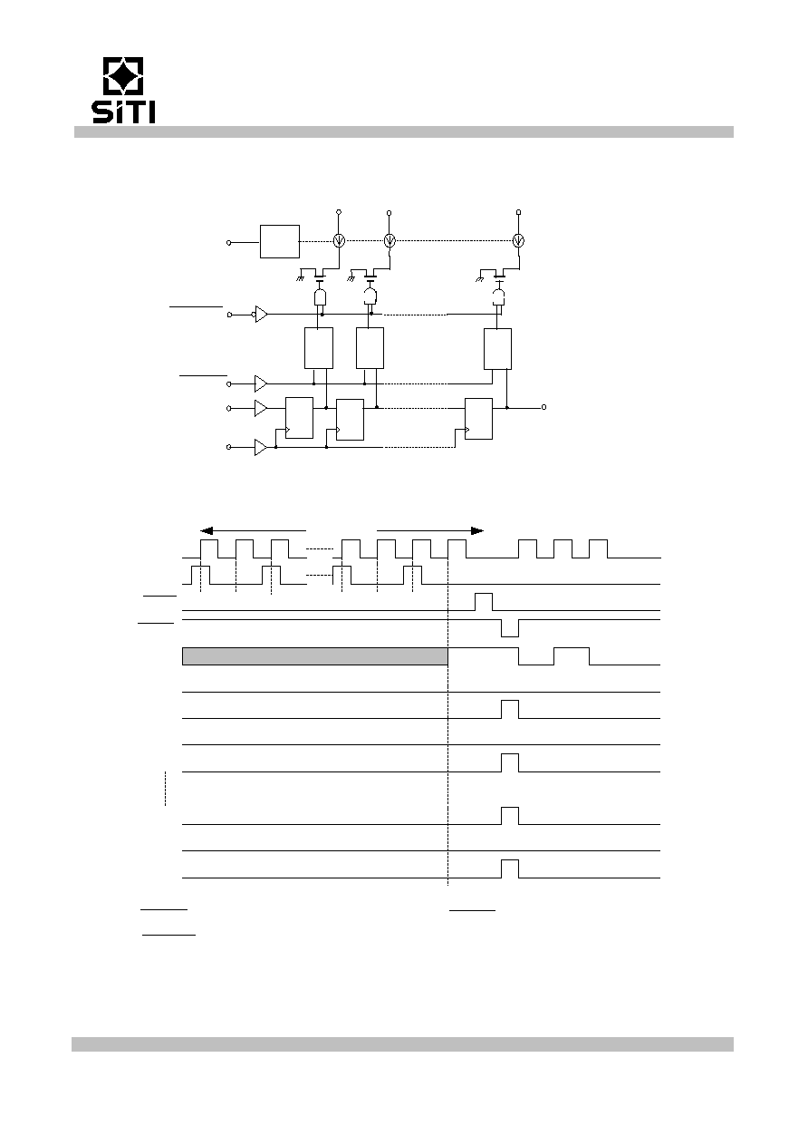
Block Diagram
Timing Diagram
(Note) Latches are level sensitive (not edge triggered).
LATCH-terminal = H level, latches become transparent; LATCH-terminal = L level, latches hold data.
ENABLE-terminal = H level, all outputs (OUT0~15) are off.
An external resistor is connected between R-EXT and GND for setting up the value of constant current.
SERIAL-OUT changes state on the rising edges of clock.
CLOCK
SERIAL_IN
LATCH
ENABLE
OUT0
OUT1
OUT2
OUT3
OUT13
OUT14
OUT15
5V
0V
5V
0V
5V
0V
5V
0V
ON
OFF
ON
OFF
ON
OFF
ON
OFF
ON
OFF
ON
OFF
ON
OFF
5V
0V
SERIAL_OUT
Previous Data
16 Clocks
CK
CK
CK
D
D
D
Q
Q
Q
D
ST
Q
CLOCK
I-REG.
SERIAL-IN
LATCH
R-EXT
SERIAL-OUT
OUT15
OUT1
OUT0
D
ST
ST
Q
Q
D
ENABLE
DM134B
DM135B
SILICON TOUCH TECHNOLOGY INC.
16-Bit Constant Current LED Drivers
-
4-
Version
A.001
Preliminary
Pin Description
PIN No.
PIN NAME
FUNCTION
1 GND
Ground
terminal
2
SERIAL-IN
Input terminal of a data shift register
3
CLOCK
Input terminal of a clock for shift register
4
LATCH
Input terminal of data strobe
5~20 OUT0~15
Output
terminals
21
ENABLE
Input terminal of output enable (active low)
22
SERIAL-OUT
Output terminal of a data shift register
23
R-EXT
Input terminal of an external resistor
24 V
DD
5V Supply voltage terminal
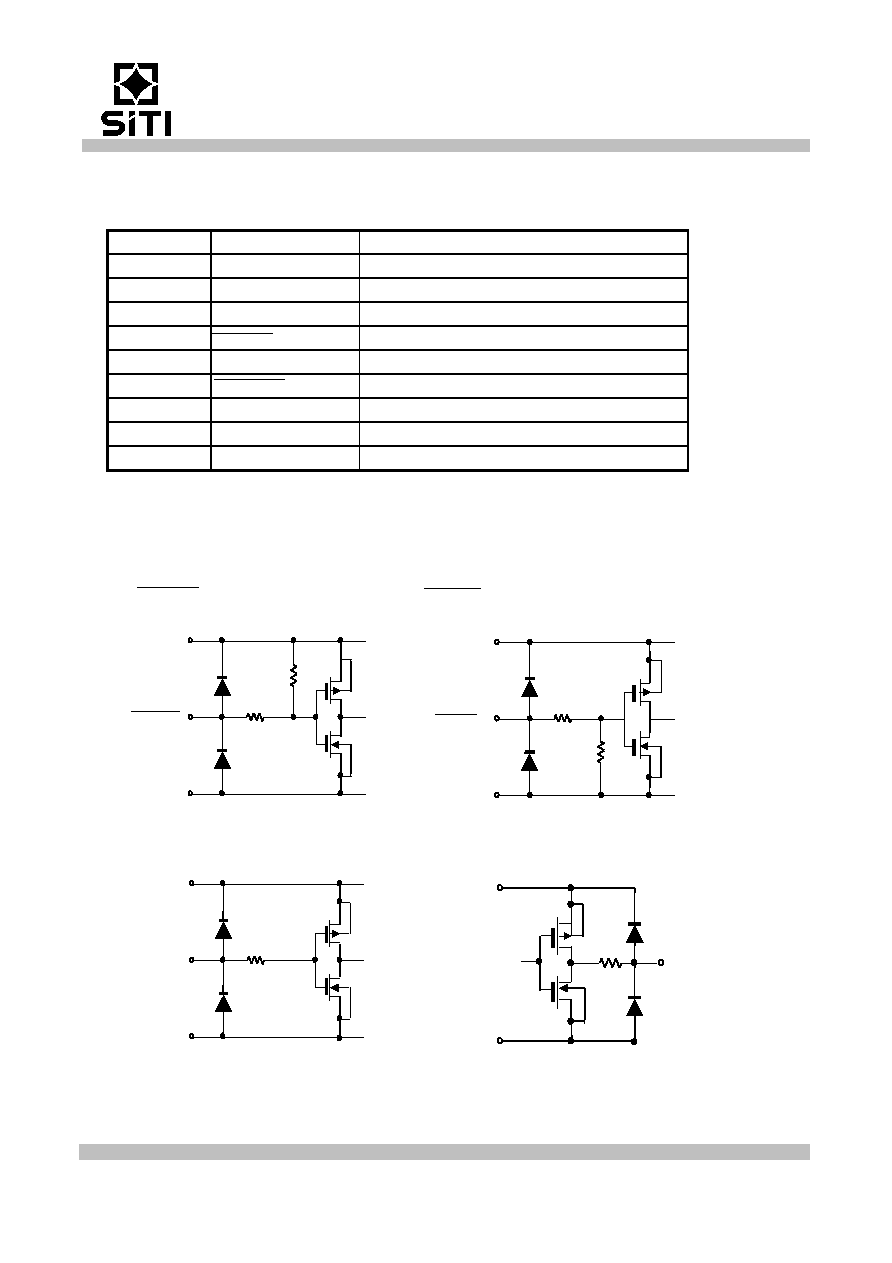
Equivalent Circuit of Inputs and Outputs
1. ENABLE terminal
2. LATCH terminal
3. CLOCK, SERIAL-IN terminal
4. SERIAL-OUT terminal
CLOCK,
SERIAL-IN
GND
V
DD
GND
V
DD
RIN (up)
ENABLE
SERIAL-OUT
GND
V
DD
LATCH
GND
V
DD
RIN