 | –≠–ª–µ–∫—Ç—Ä–æ–Ω–Ω—ã–π –∫–æ–º–ø–æ–Ω–µ–Ω—Ç: FA5511N | –°–∫–∞—á–∞—Ç—å:  PDF PDF  ZIP ZIP |
FA551X
1
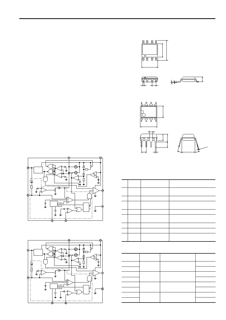
Block diagram
FA5510P (N), FA5511P (N)
FA5514P (N), FA5515P (N)
FA551X series
Dimensions, mm
SOP-8
FA5510P (N), FA5511P (N)
FA5514P (N), FA5515P (N)
Description
The FA551X series are the PWM type switching power supply
control ICs that can directly drive power MOSFET. These ICs
use a CMOS device with high dielectric strength (30V) to
implement low power consumption. These ICs contain many
function in a small 8-pin package. With these ICs, a high-
performance and compact power supply can be created
because not many external discrete components are needed.
Features
∑ Low current consumption by CMOS process with high
dielectric strength (30V)
∑ Standby current of 2µA or less (at Vcc=14V), and operating
current of 1.5mA (typ)
∑ Overvoltage protection function detecting the Vcc voltage
∑ A drive circuit for connecting a power MOSFET directly
∑ Output peak current: ±1.5A
∑ Pulse-by-pulse overcurrent limiting function
∑ Overload protection function (latch or non-latch mode selectable)
∑ Output ON-OFF function by external signal
∑ Latch-mode overvoltage shutdown function
∑ Undervoltage lockout function (16.5V ON / 9V OFF)
∑ Reference voltage output (5V)
∑ 8-pin package (DIP/SOP)
CMOS IC
For Switching Power Supply Control
4.9
3.9
6.0
±
0.2
0.4
±
0.1
1.27
0.20
+0.1
≠0.05
0~8
∞
1
4
8
5
1.8max
DIP-8
1
8
5
4
9.3
6.4
7.62
3.3
4.5max
1.5
±
0.3
3.0min
0~15∞
0~15∞
0.46
±
0.1
2.54
0.25
+0.1
≠0.05
Type
Max. duty
Polarity of overcurrent Package
cycle (typ.)
detection
FA5510P
46%
+
DIP-8
FA5510N
SOP-8
FA5511P
70%
+
DIP-8
FA5511N
SOP-8
FA5514P
46%
≠
DIP-8
FA5514N
SOP-8
FA5515P
70%
≠
DIP-8
FA5515N
SOP-8
0.8V/0.68V
8.5V/7.9V
5V VCC
ENB
5V REF
3.5V
4V
RT CT
OSC
+0.24V
R
S
QB
Q
ENB
OUT
PUT
16.5V/9V
UVLO
15.5V
15.5V
5.2
µ
A
0.95mA
PWM
0.8V
Dmax
FA5510: 46%
FA5511: 70%
5V Controlled block
FB
(2)
REF
(7)
CS(8)
VCC(6)
OUT
(5)
GND
(4)
IS+(3)
RT(1)
FF
0.8V/0.68V
8.5V/7.9V
5V VCC
ENB
5V REF
3.5V
4V
RT CT
OSC
-0.17V
R
S
QB
Q
ENB
OUT
PUT
16.5V/9V
UVLO
15.5V
15.5V
5.2
µ
A
0.95mA
PWM
0.8V
Dmax
FA5514: 46%
FA5515: 70%
5V Controlled block
FB
(2)
REF
(7)
CS(8)
VCC(6)
OUT
(5)
GND
(4)
IS-(3)
RT(1)
FF
Pin Pin
Function
Description
No. symbol
1
RT
Oscillator timing
Setting oscillation frequency
resistor
2
FB
Feedback
Input of PWM comparator
3
IS
Overcurrent
Input of the overcurrent
detection
limiting function
4
GND
Ground
Ground
5
OUT
Output
Output for driving a power
MOSFET
6
VCC
Power supply
Power supply
7
REF
Reference voltage
Reference voltage output (5V)
8
CS
Soft-start and
Soft-start, ON/OFF function and
ON/OFF control
latch-mode shutdown operations
FA551X
2
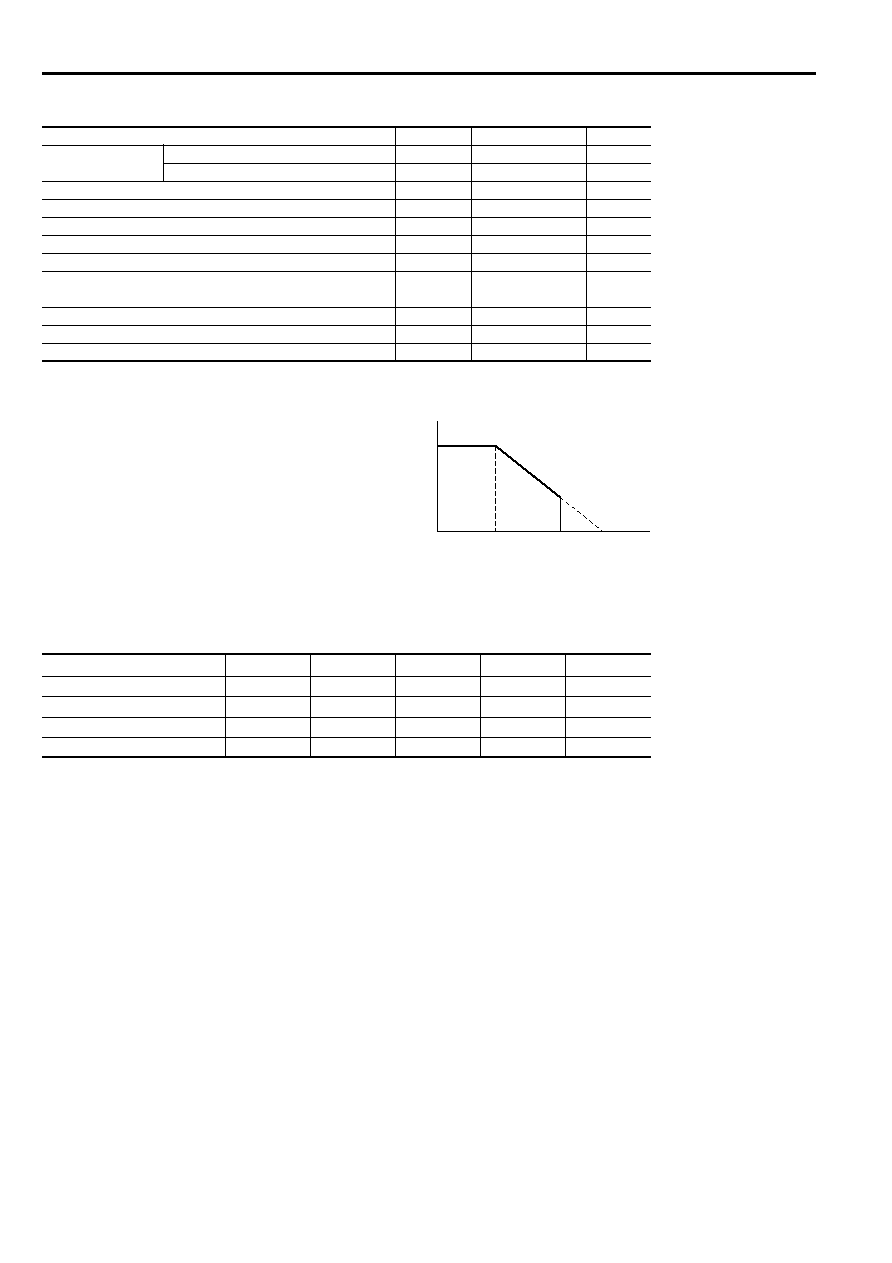
Maximum power dissipation curve
Absolute maximum ratings
I
tem
Symbol
Rating
Unit
Supply Voltage
Low impedance source (I
CC
>15mA)
V
CC1
30
V
Internal zener clamp (I
CC
<15mA)
V
CC2
Self limiting
V
Output peak current
I
OUT
±1.5
A
FB pin input voltage
V
FB
≠0.3 to 5.0
V
IS pin input voltage
V
IS
≠0.3 to 5.0
V
REF pin source current
I
REF
≠10
mA
CS pin sink current
I
CS
+2.0
mA
Total power dissipation (Ta=25∞C)
Pd
800 (DIP-8)
mW
400 (SOP-8)
Ambient temperature
Ta
≠30 to +85
∞C
Maximum junction temperature
Tj
125
∞C
Storage temperature
Tstg
≠40 to +150
∞C
Note: There are cases where the IC cannot output the rating current depending on Vcc voltage or temperature.
≠30
25
85
125
0
Ambient temperature Ta [∞C]
Max.
po
w
er
dissipation
400mW (SOP)
800mW (DIP)
Recommended operating conditions
Item
Symbol
Min.
Typ.
Max.
Unit
Supply voltage
V
CC
10
28
V
Oscillation frequency
f
OSC
10
500
kHz
REF-GND capacitor
Cref
0.1
0.47
µF
Soft start capacitor
C
S
0.01
1
µF
FA551X
3
Electrical characteristics (V
CC
=18V, R
T
=47k
, Ta=25∞C)
Reference voltage section (REF pin)
Item
Symbol
Test condition
Min.
Typ.
Max.
Unit
Reference voltage
V
REF
Tj=25∞C
4.75
5.00
5.25
V
Line regulation
V
dv1
V
CC
=10 to 28V
±6
±20
mV
Load regulation
V
dv2
I
L
=0 to 10mA, V
CC
=18V
≠40
≠12
mV
Temperature stability
V
dT
Ta=≠30 to 85∞C
±0.5
mV/∞C
Oscillator section (RT pin)
Item
Symbol
Test condition
Min.
Typ.
Max.
Unit
Oscillation frequency
f
OSC
R
T
=47k
, Tj=25∞C
92.6
100
107.4
kHz
Voltage stability
f
dv
V
CC
=10 to 28V
±1.0
%
Temperature stability
f
dT
Ta=≠30 to 85∞C
±0.02
%/∞C
Pulse width modulation circuit section (FB pin)
Item
Symbol
Test condition
FA5510/14
FA5511/15
Unit
Min.
Typ.
Max.
Min.
Typ.
Max.
FB pin source current
I
FB
V
FB
=0
≠855
≠720
≠585
≠855
≠720
≠585
µA
Input threshold voltage (FB pin)
V
TH FB0
Duty cycle =0%
0.9
1
0.9
1
V
V
TH FBM
Duty cycle =
D
MAX
1.92
2.40
V
Maximum duty cycle
D
MAX
42
46
50
66
70
74
%
Overcurrent limiting circuit section (IS pin)
Item
Symbol
Test condition
FA5510/11
FA5514/15
Unit
Min.
Typ.
Max.
Min.
Typ.
Max.
Input threshold voltage (IS pin)
V
THIS
220
240
260
≠190
≠170
≠150
mV
Source current (IS pin)
I
IS
V
IS
=0V
±5
≠28
≠20
≠12
µA
Delay time
t
pdIS
150
150
ns
Output ON/OFF control circuit section (CS pin)
Item
Symbol
Test condition
Min.
Typ.
Max.
Unit
Source current (CS pin)
I
S0CS
V
CS
=0V, Tj=25∞C
≠7.2
≠5.2
≠3.2
µA
ON/OFF control threshold voltage (CS pin)
V
THON
OFF
ON, Tj=25∞C
0.8
0.93
V
V
THOFF
ON
OFF, Tj=25C
0.50
0.68
V
Hysteresis voltage
V
THOHS
0.12
V
Soft start circuit section (CS pin)
Item
Symbol
Test condition
FA5310/14
FA5311/15
Unit
Min.
Typ.
Max.
Min.
Typ.
Max.
Charge current (CS pin)
I
CHG
V
CS
=1V, Tj=25∞C ≠7.2
≠5.2
≠3.2
≠7.2
≠5.2
≠3.2
µA
Input threshold voltage (CS pin)
V
TH CS0
Duty cycle =0%
0.90
1.0
0.90
1.0
V
V
TH CSM
Duty cycle =
D
MAX
1.92
2.40
V

FA551X
4
Overload cutoff circuit section (FB pin)
Item
Symbol
Test condition
Min.
Typ.
Max.
Unit
Overload threshold voltage (FB pin)
V
TH FB
3.2
3.5
3.8
V
Overvoltage cutoff circuit section (VCC pin)
Item
Symbol
Test condition
Min.
Typ.
Max.
Unit
Overvoltage threshold voltage (VCC pin)
V
TH VCC
Tj=25∞C
30
31.8
34
V
Cutoff operating supply current (VCC pin)
I
VCC
Tj=25∞C, V
CC
=V
THVCC
14
mA
Charge current (CS pin)
I
S0CS2
V
CS
=6.5V
≠1.4
≠0.95
≠0.5
mA
Undervoltage lockout circuit section (VCC pin)
Item
Symbol
Test condition
Min.
Typ.
Max.
Unit
OFF-to-ON threshold voltage
V
CC ON
Tj=25∞C
15.5
16.5
17.5
V
ON-to-OFF threshold voltage
V
CC OFF
Tj=25∞C
8.5
9.0
10.0
V
Hysteresis voltage
V
HYS
Tj=25∞C
6.8
7.5
8.2
V
Output circuit section (OUT pin)
Item
Symbol
Test condition
Min.
Typ.
Max.
Unit
Low output voltage
V
OL
I
OL
=100mA
0.7
1.5
V
High output voltage
V
OH
I
OH
=≠100mA, V
CC
=18V
15
16.5
V
Rise time
tr
C
L
=1nF
40
ns
Fall time
tf
C
L
=1nF
25
ns
Latch-mode cutoff circuit section (CS pin)
Item
Symbol
Test condition
Min.
Typ.
Max.
Unit
Sink current (CS pin)
I
SICS
V
CS
=6.5V, V
FB
=1V, Tj=25∞C
18
30
45
µA
Cutoff threshold voltage (CS pin)
V
TH CSF
ON
OFF, Tj=25∞C
8.0
8.5
9.0
V
V
TH CSN
OFF
ON, Tj=25∞C
7.4
7.9
8.4
V
Hysteresis voltage
V
THHIS
0.6
V
Supply current (VCC pin)
Item
Symbol
Test condition
Min.
Typ.
Max.
Unit
Stand-by current
I
CCSTB
V
CC
=14V
2
µA
Startup current
I
CCST
V
CC
=OFF-to-ON threshold voltage
12
30
µA
Operating-state supply current
I
CCOP
No load
1.5
2.5
mA
OFF-state supply current
I
CCOF
V
CC
=17V, CS=0V
80
200
µA
Latch mode supply current
I
CCL
V
CC
=10V
45
80
µA

FA551X
5
Characteristic curves (V
CC
=18V, R
T
=47k
, Ta=25∞C)
Oscillation frequency (f
OSC
) vs.
Oscillation frequency (f
OSC
) vs. supply voltage (V
CC
)
timing resistor resistance (R
T
)
Oscillation frequency (f
OSC
) vs.
FB pin source current (I
FB
) vs. FB pin voltage (V
FB
)
junction temperature (Tj)
Maximum duty cycle (D
MAX
) vs. timing resitor resistance (R
T
)
Maximum duty cycle (D
MAX
) vs. timing resitor resistance (R
T
)
FA5510/14
FA5511/15
1
10
100
1000
1
10
100
1000
R
T
(k
)
fosc (kHz)
99.9
99.92
99.94
99.96
99.98
100
100.02
100.04
100.06
100.08
100.1
10
15
20
25
30
Vcc (V)
fosc (kHz)
98.5
99
99.5
100
100.5
101
101.5
102
≠50
0
50
100
150
Tj (∞C)
fosc (kHz)
-800
-700
-600
-500
-400
-300
-200
-100
0
0
1
2
3
4
5
V
FB
(V)
I
FB
(
µ
A)
42
43
44
45
46
47
48
49
1
10
100
1000
R
T
(k
)
D
MAX
(%)
67
68
69
70
71
72
1
10
100
1000
R
T
(k
)
D
MAX
(%)