
Regarding the change of names mentioned in the document, such as Hitachi
Electric and Hitachi XX, to Renesas Technology Corp.
The semiconductor operations of Mitsubishi Electric and Hitachi were transferred to Renesas
Technology Corporation on April 1st 2003. These operations include microcomputer, logic, analog
and discrete devices, and memory chips other than DRAMs (flash memory, SRAMs etc.)
Accordingly, although Hitachi, Hitachi, Ltd., Hitachi Semiconductors, and other Hitachi brand
names are mentioned in the document, these names have in fact all been changed to Renesas
Technology Corp. Thank you for your understanding. Except for our corporate trademark, logo and
corporate statement, no changes whatsoever have been made to the contents of the document, and
these changes do not constitute any alteration to the contents of the document itself.
Renesas Technology Home Page: http://www.renesas.com
Renesas Technology Corp.
Customer Support Dept.
April 1, 2003
To all our customers

Cautions
Keep safety first in your circuit designs!
1. Renesas Technology Corporation puts the maximum effort into making semiconductor products better
and more reliable, but there is always the possibility that trouble may occur with them. Trouble with
semiconductors may lead to personal injury, fire or property damage.
Remember to give due consideration to safety when making your circuit designs, with appropriate
measures such as (i) placement of substitutive, auxiliary circuits, (ii) use of nonflammable material or
(iii) prevention against any malfunction or mishap.
Notes regarding these materials
1. These materials are intended as a reference to assist our customers in the selection of the Renesas
Technology Corporation product best suited to the customer's application; they do not convey any
license under any intellectual property rights, or any other rights, belonging to Renesas Technology
Corporation or a third party.
2. Renesas Technology Corporation assumes no responsibility for any damage, or infringement of any
third-party's rights, originating in the use of any product data, diagrams, charts, programs, algorithms, or
circuit application examples contained in these materials.
3. All information contained in these materials, including product data, diagrams, charts, programs and
algorithms represents information on products at the time of publication of these materials, and are
subject to change by Renesas Technology Corporation without notice due to product improvements or
other reasons. It is therefore recommended that customers contact Renesas Technology Corporation
or an authorized Renesas Technology Corporation product distributor for the latest product information
before purchasing a product listed herein.
The information described here may contain technical inaccuracies or typographical errors.
Renesas Technology Corporation assumes no responsibility for any damage, liability, or other loss
rising from these inaccuracies or errors.
Please also pay attention to information published by Renesas Technology Corporation by various
means, including the Renesas Technology Corporation Semiconductor home page
(http://www.renesas.com).
4. When using any or all of the information contained in these materials, including product data, diagrams,
charts, programs, and algorithms, please be sure to evaluate all information as a total system before
making a final decision on the applicability of the information and products. Renesas Technology
Corporation assumes no responsibility for any damage, liability or other loss resulting from the
information contained herein.
5. Renesas Technology Corporation semiconductors are not designed or manufactured for use in a device
or system that is used under circumstances in which human life is potentially at stake. Please contact
Renesas Technology Corporation or an authorized Renesas Technology Corporation product distributor
when considering the use of a product contained herein for any specific purposes, such as apparatus or
systems for transportation, vehicular, medical, aerospace, nuclear, or undersea repeater use.
6. The prior written approval of Renesas Technology Corporation is necessary to reprint or reproduce in
whole or in part these materials.
7. If these products or technologies are subject to the Japanese export control restrictions, they must be
exported under a license from the Japanese government and cannot be imported into a country other
than the approved destination.
Any diversion or reexport contrary to the export control laws and regulations of Japan and/or the
country of destination is prohibited.
8. Please contact Renesas Technology Corporation for further details on these materials or the products
contained therein.

HA16129AFPJ
Single Watchdog Timer
ADE-204-067 (Z)
Rev. 0
Mar. 2001
Description
The HA16129AFPJ is a watchdog timer IC that monitors a microprocessor for runaway. In addition to the
watchdog timer function, the HA16129AFPJ also provides a function for supplying a high-precision
stabilized power supply to the microprocessor, a power on reset function, a power supply voltage
monitoring function, and a fail-safe function that masks the microprocessor outputs if a runaway is
detected.
Functions
∑
Watchdog timer (WDT) function
Monitors the P-RUN signal output by the microprocessor, and issues an auto-reset (
RES) signal if a
microprocessor runaway is detected.
∑
Stabilized power supply
Provides power to the microprocessor.
∑
Power on and clock off functions
The power on function outputs a low level signal to the microprocessor for a fixed period when power
is first applied.
The clock off function outputs a
RES signal to the microprocessor a fixed period after a runaway
occurs.
∑
Power supply monitoring function
When the reference voltage (Vout) falls and becomes lower than the
NMI detection voltage (4.63 V,
Typ) or the
STBY detection voltage (3.0 V Typ), this function outputs either an NMI signal or an STBY
signal, respectively. Note that NMI detection can be set to monitor either V
CC
or Vout.
∑
OUTE function
*1
(fail-safe function)
Outputs a signal used to mask microprocessor outputs when a microprocessor runaway has been
detected.
∑
RES delay function
Sets the delay between the time the
NMI signal is output and the time the RES signal is output.
∑
Protection functions
The HA16129AFPJ incorporates both Vout overvoltage prevention and short detection functions.
Note: 1. OUTE function: OUTE is an abbreviation for output enable.

HA16129AFPJ
2
Features
∑
High-precision output voltage: 5.0 V
±
1.5%
∑
The WDT supports both frequency and duty detection schemes.
∑
High-precision power supply monitoring function: 4.625 V
±
0.125 V
∑
Built-in OUTE function
∑
All functions can be adjusted with external resistors and/or capacitors.
Pin Arrangement
(Top view)
V
CC
STBY
1
2
3
4
5
6
7
8
9
10
P-RUN
Rf
Cf
GND
Voadj
OUTE
20
19
18
17
16
15
14
13
12
11
STBYadj
NMIadj
NMIsns
CONT
CS
V
OUT
C
RES
R
R
C
R
R
T
RES
NMI
HA16129AFPJ
3
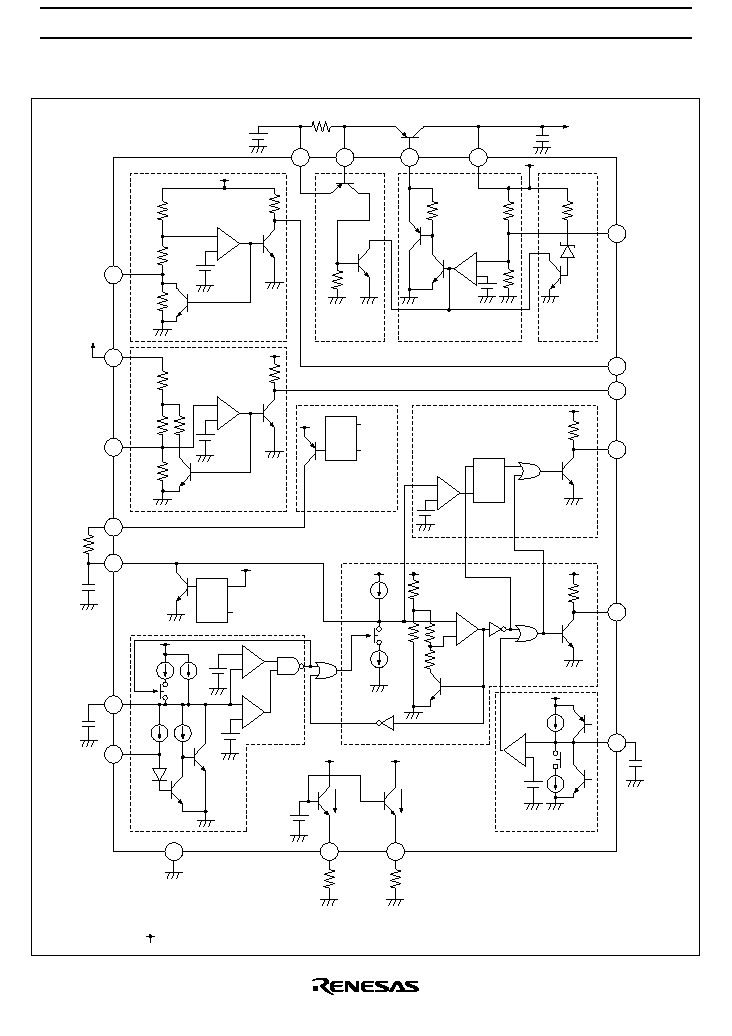
Block Diagram
-
+
71k
1.5V
STBY
detection
block
36.8k
-
+
2k
NMI
detection
block
25k
1.18V
70k
80k
3.3k
19
15
STBYadj
NMIsns
16
NMIadj
To Vout
31.2k
Q
R
S
RES
STBY
t
ON
detection
block
6
R
T
5
C
R
Q
R
S
NMI
3
Cf
If*16
If/6
1
P-RUN
-
+
-
+
-
WDT block
I
R
I
R
*4/3
Delay circuit block
-
8.4k
20k
33k
19k
18
3.3k
+
-
+
7
C
RES
RES
-
+
Q
R
S
OUTE
block
10
3.3k
OUTE
17
NMI
20
STBY
11
12
13
Regulator block
+
-
V
CC
CS
CONT
Short
detection
block
9
Voadj
14
V
OUT
To microprocessor
(or other device)
power supply
connections
RES
block
4
R
R
2
Rf
I
R
If
2V
8
GND
3.3k
1.24V
Overvoltage
detection
block
Note: The current, voltage, and resistor values listed in the diagram are reference values.
: Connect to Vout

HA16129AFPJ
4
Pin Function
Related
Function
Pin
No.
Symbol
Function
WDT.
1
P-RUN
Watchdog timer pulse input. The auto-reset function is controlled by the
duty cycle or frequency of this input pulse signal.
2
Rf
The resistor connected to this pin determines the current that flows in the
Cf pin capacitor. Use the resistor value from 100 k
to 500 k
3
Cf
The current determined by the Rf pin charges the Cf capacitor and the
potential on this pin determines the watchdog timer frequency band.
t
RH
, t
RL
, t
OFF
4
R
R
The resistor connected to this pin determines the current that flows in the
C
R
pin capacitor. Use the resistor value from 100 k
to 500 k
5
C
R
The current determined by the R
R
pin charges the capacitor C
R
and the
potential on this pin controls the
RES
function (toff, t
RH
, and t
RL
).
t
ON
6
R
T
The resistor R
T
, which determines only the time t
ON
for the
RES
function is
connected to this pin. This resistor determines the current that charges the
capacitor C
R
for the time t
ON
. Use the resistor value from 100 k
to 500 k
tr, t
RES
7
C
RES
The current determined by the Rf pin charges the capacitor C
RES
, and the
RES
delay times (Tr and T
RES
) are determined by the potential of this
capacitor.
--
8
GND
Ground
Vout
9
Voadj
Insert the resistor Roadj if fine adjustment of the regulator output voltage
Vout is required. Leave this pin open if Vout does not need to be changed.
Output
10
OUTE
Output for the OUTE function
Power
supply
11
V
CC
Power supply
Short
detection
12
CS
Connect the overcurrent detection resistor between the CS pin and the V
CC
pin. If this function is not used, short this pin to V
CC
. Also, connect this pin
to the emitter of the external transistor.
Vout
13
CONT
Connect this pin to the base of the external transistor.
14
V
OUT
Provides the regulator output voltage and the IC internal power supply.
Connect this pin to the collector of the external transistor.
NMI
15
NMIsns
This pin senses the
NMI
detection voltage. If V
CC
is to be detected,
connect this pin to the V
CC
pin (however, note that an external resistor is
required), and if Vout is to be detected, connect this pin to the V
OUT
pin.
16
NMIadj
Insert a resistor if fine adjustment of the
NMI
detection voltage is required.
Leave this pin open if fine adjustment is not required.
Output
17
NMI
NMI
output
Output
18
RES
RES
output
STBY
19
STBYadj
Insert a resistor if fine adjustment of the
S T B Y
detection voltage is
required. Leave this pin open if fine adjustment is not required.
Output
20
STBY
STBY
output

HA16129AFPJ
5
Functional Description
This section describes the functions provided by the HA16129FPJ. See the section on formulas for details
on adjustment methods.
Regulator Block
Vout Voltage
This IC provides a stabilized 5 V power supply by controlling the base current of an external transistor. The
largest current (the maximum CONT pin current) that can be drawn by the base of this external transistor is
20 mA. Also note that the Vout output is also used for the power supply for this IC's internal circuits.
Short Detection Block
When a current detection resistor (R
CS
) is connected between the V
CC
pin and the CS pin, and the voltage
between these pins exceeds the V
CS
voltage (700 mV Typ), the CONT pin function turns off and the output
voltage supply is stopped.
Output Voltage (Vout) Adjustment
The output voltage can be adjusted by connecting an external resistor at the output voltage adjustment pin
(Voadj). However, if for some reason the voltage on this Vout line increases and exceeds the voltage
adjustment range (7 V Max), the CONT pin function turns off and the output voltage supply is stopped.
Refer to the timing charts in conjunction with the following items.
LVI (Low Voltage Inhibit)
NMI Detection Voltage
This function monitors for drops in the power-supply voltage. This function can be set up to monitor either
V
CC
or Vout. When Vout is monitored, a low level is output from the
NMI pin if that voltage falls under the
detection voltage (4.63 V Typ). Then, when the power-supply voltage that fell rises again, the
NMI pin
will output a high level. Note that this function has a fixed hysteresis of 50 mV (Typ). The monitored
power supply is selected by connecting the NMIsns pin either to the V
CC
pin or to the V
OUT
pin. When
detecting V
CC
, an external adjustment resistor is required.)
The detection voltage can also be adjusted with the NMIadj pin.
STBY Detection Voltage
This function monitors for drops in the Vout voltage. It monitors the Vout voltage, and outputs a low level
from the
STBY pin if that voltage drops below the detection voltage (3.0 V Typ). Then, when the power-
supply voltage that fell rises again, the
STBY pin will output a high level. Note that this function has a
fixed hysteresis of 1.35 V (Typ).
The detection voltage can also be adjusted with the STBYadj pin.

HA16129AFPJ
6
Function Start Voltage
This is the minimum required Vout voltage for the
RES, NMI, STBY, and OUTE output pin functions to
start operating. It is stipulated as the voltage that Vout must reach after power is first applied for these pins
to output a low level.
Hysteresis
This is the difference between the LVI function detection voltage when the power-supply voltage drops,
and the clear (reset) voltage when the power-supply voltage rises.
(V
HYSN
= V
NMI
'
-
V
NMI
; V
HYSS
= V
STBY
'
-
V
STBY
)
OUTE Function
When a microprocessor is in the runaway state, its outputs are undefined, and thus it is possible that the
outputs may be driven by incorrect signals. This function is used to mask such incorrect microprocessor
outputs. When the WDT function recognizes normal operation (when the
RES output is high), the OUTE
output will be held high. When the WDT function recognizes an abnormal state and an auto-reset pulse is
output from the
RES pin, the OUTE output will be held low. Thus microprocessor outputs during
microprocessor runaway can be masked by taking the AND of those outputs and this signal using external
AND gates.
The OUTE output will go high when the C
R
pin voltage exceeds VthHcr2, and will go low when that
voltage falls below VthLcr.
There are limitation that apply when the OUTE function is used. Refer to the calculation formulas item for
details.
RES Function
t
RH
This period is the length of the high-level output period of the
RES pulse when the P-RUN signal from the
microprocessor stops. This is the time required for the C
R
potential to reach VthLcr from VthHcr1.
t
RL
This period is the length of the low-level output period of the
RES pulse when the P-RUN signal from the
microprocessor stops. This is the time required for the C
R
potential to reach VthHcr1 from VthLcr.
t
OFF
This is the time from the point the P-RUN signal from the microprocessor stops to the point a low level is
output from the
RES pin. During normal microprocessor operation, the potential on the C
R
pin will be
about Vout
-
0.2 V (although this value may change with the P-RUN signal input conditions, so it should
be verified in the actual application circuit) and t
OFF
is the time for the C
R
pin potential to reach VthLcr
from that potential.

HA16129AFPJ
7
t
ON
t
ON
is the time from the point the
NMI output goes high when power is first applied to the point the RES
output goes low. t
ON
is the time for the potential of the C
R
pin to reach VthHcr1 from 0 V.
tr
The time tr is the fixed delay time between the point the
NMI output goes from low to high after the power-
supply voltage comes up to the point
RES goes from low to high. The time tr is the time for the CRES pin
potential to fall from the high voltage (about 1.9 V) to Vthcres.
t
RES
The time t
RES
is the fixed delay time between the point the
NMI output goes from high to low when the
power-supply voltage falls to the point
RES goes from high to low. The time t
RES
is the time for the C
RES
pin
potential to rise from 0 V to Vthcres.
WDT Function
This function determines whether the microprocessor is operating normally or has entered a runaway state
by monitoring the duty or frequency of the P-RUN signal. When this function recognizes a runaway state,
it outputs a reset pulse from the
RES pin and sets the OUTE pin to low from high. It holds the RES and
OUTE pins fixed at high as long as it recognizes normal microprocessor operation.
In this function, the potential of the Cf capacitor is controlled by the P-RUN signal. This Cf pin potential
charges the capacitor C
R
that controls the reset pulse to be between VthLcf and VthHcf. The judgment as
to whether or not the microprocessor is operating normally, is determined by the balance between the
charge and discharge voltage on the capacitor C
R
at this time.

HA16129AFPJ
8
Calculation Formulas
Item
Formula
Notes
Reference
voltage
Vout = 1.225 1 +
R1, R2; k
37 // R1
12 // R2
(
(
While the Vout voltage will be 5 V
±
1.5% when the
Voadj pin is open, the circuit shown here should be
used to change the Vout voltage externally.
Voadj
V
CC
CS
Vout
R2
R1
Short
detection
voltage
V
CS
(700 mV Typ)
<
I
L
R
CS
When this function operates, the base current to the
external transistor connected to the CS pin stops and
the Vout output is lowered.
V
CC
CS
Vout
R
CS
I
L
OVP
--
This function prevents the microprocessor from being
damaged if the Vout voltage is inadvertently increased
to too high a level. The OVP detection voltage is fixed.
t
RH
, t
RL
t
RH
t
RL
= 3.3
◊
C
R
R
R
= 1.1
◊
C
R
R
R
These determine the reset pulse frequency and duty.
RES
t
RH
t
RL
t
ON
t
ON
= 1.1
◊
C
R
R
T
Sets the time from the rise of the
NMI
signal to the point
the
RES
output is cleared.
NMI
t
ON
RES
t
OFF
t
OFF
= 6.5
◊
C
R
R
R
Sets the time from the point the P-RUN pulse stops to
the point a reset pulse is output.
RES
toff
P-RUN

HA16129AFPJ
9
Calculation Formulas (cont)
Item
Formula
Notes
V
STBY
V
STBY
= 1.48
◊
67.6
29.5 + 36.2 // R1
+ 1
(
(
The voltage at which the
STBY
signal is output when
Vout falls. The
STBY
detection voltage can be adjusted
by connecting a resistor between the STBYadj pin and
ground (R3). However, the
STBY
recovery voltage
cannot be adjusted.
STBY
V
STBY
V
STBY
'
Vout
t
STBYadj
Vout
STBY
R1
V
NMI
(Vout
detection)
V
NMI
= 1.2
◊
1 +
R1, R2; k
R1 // 73
R2 // 25
(
(
The voltage at which the
NMI
signal is output when
Vout falls. (When NMIsns is connected to Vout.)
The
N M I
detection voltage can be adjusted by
connecting resistors between the NMIadj pin and Vout
(R1), and between the NMIadj pin and ground (R2).
NMI
V
NMI
V
NMI
'
Vout
t
Vout
R1
NMI
NMIsns
NMIadj
R2
GND
V
NMI
(V
CC
detection)
V
NMI
= 4.62
◊
Recovery voltage
R1
R2 // 97.1
(
(
+ 1
V
NMI
= 4.68
◊
R1, R2; k
R1
R2 // 45.5
(
(
+ 1
The voltage at which the
NMI
signal is output when V
CC
falls. (When NMIsns is connected to V
CC
.)
The
N M I
detection voltage can be adjusted by
connecting resistors between the NMIsns pin and V
CC
(R1), and between the NMIsns pin and ground (R2).
NMI
V
NMI
V
NMI
'
V
CC
t
Vout
NMI
NMIsns
R2
GND
R1
V
CC
CS
OUTE
C
R
◊
R
R
>
19.3
◊
Cf
◊
Rf
If the OUTE function is used, the relationship shown at
the left must be fulfilled to assure that pulses are not
incorrectly generated in this output when a
microprocessor runaway state is detected.
HA16129AFPJ
10
Calculation Formulas (cont)
Item
Formula
Notes
WDT.
f
Line1
=
f
Line2
= 24% (fixed)
f
Line3
=
f
Line4
= 99%
The relationship between
f
Line1
and f
Line3
f
Line1
= f
Line3
◊
12.9 (Du
-
24)
0.31
◊
(Du
-
24)
Cf
Rf
0.024
Cf
Rf
The WDT function judges whether the P-RUN pulse
signal is normal or not. If the WDT function judges the
P-RUN pulse signal to be abnormal, it outputs a reset
signal. The normal range is the area enclosed by f
Line1
to
f
Line4
in the figure.
t
L
t
H
Du: The P-RUN signal duty cycle
Du =
◊
100
t
H
t
H
+ t
L
f
Line1
Duty
Frequency
Normal
operation
area
f
Line2
f
Line3
f
Line4
HA16129AFPJ
11
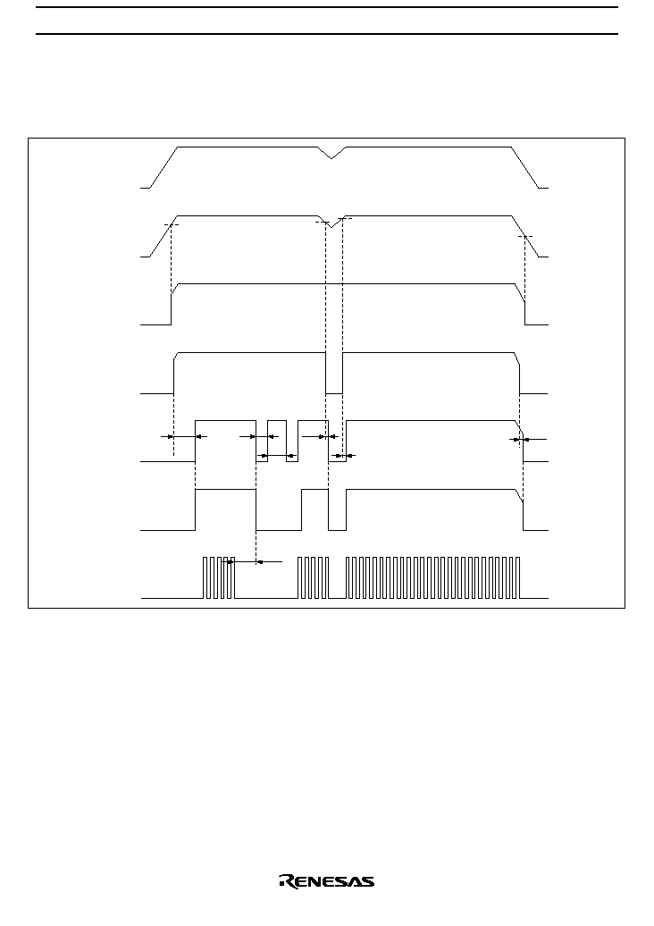
Timing Charts
Whole system timing chart
t
OFF
V
CC
t
ON
t
RL
t
RH
tr
t
RES
t
RES
Microprocessor
runaway
V
STBY
'
V
NMI
V
NMI
'
V
STBY
V
OUT
STBY
NMI
RES
OUTE
P-RUN
HA16129AFPJ
12
WDT. timing chart
Cf
Normal
operation
High-frequency
runaway
Low-frequency runaway
P-RUN
VthHcf
VthLcf
C
R
RES
OUTE
V
OUT
VthHcr2
t
RH
t
OFF
t
RL
VthHcr1
VthLcr
(5 V)
LVI timing chart
V
CC
t
ON
V
STBY
'
V
NMI
V
NMI
'
V
STBY
V
OUT
STBY
NMI
RES
&
OUTE
C
RES
tr
t
RES
Vthcres
C
R

HA16129AFPJ
13
Absolute Maximum Ratings (Ta = 25
∞
C)
Item
Symbol
Rating
Unit
Power supply voltage
V
CC
40
V
CS pin voltage
V
CS
V
CC
V
CONT pin current
Icont
20
mA
CONT pin voltage
Vcont
V
CC
V
Vout pin voltage
Vout
12
V
P-RUN pin voltage
V
PRUN
Vout
V
NMIsns pin voltage
V
NMIsns
V
CC
V
NMI
pin voltage
V
NMI
Vout
V
STBY
pin voltage
V
STBY
Vout
V
RES
pin voltage
V
RES
Vout
V
OUTE pin voltage
V
OUTE
Vout
V
Power dissipation
*1
P
T
400
mW
Operating temperature
Topr
-
40 to +85
∞
C
Storage temperature
Tstg
-
50 to +125
∞
C
Note:
1. This is the allowable value when mounted on a 40
◊
40
◊
1.6 mm glass-epoxy printed circuit
board with a mounting density of 10% at ambient temperatures up to Ta = 77
∞
C. This value must
be derated by 8.3 mW/
∞
C above that temperature.
400
300
200
100
0
Power Dissipation P
T
(mW)
Ambient Temperature Ta (
∞
C)
77
∞
C
85
∞
C
0
20
40
60
80
-
20
-
40
140
100
120

HA16129AFPJ
14
Electrical Characteristics (Ta = 25
∞
C, V
CC
= 12V, Vout = 5.0V, Rf = R
R
= 180k
, Cf =
3300pF, C
R
= 0.1
µ
F, R
T
= 390k
, C
RES
= 1500pF, R
CS
= 0.2
)
Item
Symbol
Min
Typ
Max
Unit
Test
conditions
Power supply current
I
CC
10
15
mA
Short detection voltage
V
CS
400
700
900
mV
V
CS
= (V
CC
pin
voltage
-
CS pin
voltage)
Regulator
block
Output voltage
Vout
4.925
5.00
5.075
V
V
CC
= 12V,
Icont = 5mA
Input voltage stabilization Volin
-
30
30
mV
V
CC
=
6 to 17.5V,
Icont = 10mA
Load current stabilization Voload
-
30
30
mV
Icont =
0.1 to 15mA
Ripple exclusion ratio
R
REJ
(45)
75
dB
Vi = 0.5Vrms,
fi = 1kHz
Output voltage
temperature coefficient
|
Vout/
T
|
40
(200)
ppm/
∞
C Icont = 5mA
Output voltage
adjustment range
V
oMAX
7.0
V
P-RUN
input block
Input high-level voltage
V
iH
2.0
V
Input low-level voltage
V
iL
0.8
V
Input high-level current
I
iH
300
500
µ
A
V
iH
= 5.0V
Input low-level current
I
iL
-
5
0
5
µ
A
V
iL
= 0.0V
NMI
output
block
High level
V
OHN
Vout
-
0.2 Vout
Vout + 0.2 V
I
OHN
= 0mA
Low level
V
OLN
0.4
V
I
OLN
= 2.0mA
Function start voltage
V
STN
0.7
1.4
V
STBY
output
block
High level
V
OHS
Vout
-
0.2 Vout
Vout + 0.2 V
I
OHS
= 0mA
Low level
V
OLS
0.4
V
I
OLS
= 2.0mA
Function start voltage
V
STS
0.7
1.4
V
Note:
Values in parentheses are design reference values.

HA16129AFPJ
15
Electrical Characteristics (Ta = 25
∞
C, V
CC
= 12V, Vout = 5.0V, Rf = R
R
= 180k
, Cf =
3300pF, C
R
= 0.1
µ
F, R
T
= 390k
, C
RES
= 1500pF, R
CS
= 0.2
) (cont)
Item
Symbol
Min
Typ
Max
Unit
Test
conditions
RES
output
block
High level
V
OHR
Vout
-
0.2 Vout
Vout + 0.2 V
I
OHR
= 0mA
Low level
V
OLR
0.4
V
I
OLR
= 2.0mA
Function start voltage
V
STR
0.7
1.4
V
OUTE
output
block
High level
V
OHE
Vout
-
0.2 Vout
Vout + 0.2 V
I
OHE
= 0mA
Low level
V
OLE
0.4
V
I
OLE
= 2.0mA
Function start voltage
V
STE
0.7
1.4
V
RES
function
Power on time
ton
25
40
60
ms
Clock off time
toff
80
130
190
ms
Reset pulse high time
t
RH
40
60
90
ms
Reset pulse low time
t
RL
15
20
30
ms
LVI
function
NMI
function
(Vout
detection)
Detection
voltage 1
V
NMI1
4.5
4.63
4.75
V
Hysteresis 1 V
HYSN1
50
100
mV
Temperature
coefficient
|
V
NMI
/
T
|
100
(400)
ppm/
∞
C
NMI
function
(V
CC
detection)
Detection
voltage 2
V
NMI2
5.0
5.4
5.7
V
R1 = 13k
,
R2 = 390k
Hysteresis 2 V
HYSN2
0.5
0.8
1.3
V
R1 = 13k
,
R2 = 390k
STBY
function
Detection
voltage
V
STBY
2.70
3.00
3.30
V
Hysteresis
V
HYSS
1.20
1.35
1.50
V
Temperature
coefficient
|
V
STBY
/
T
|
100
(400)
ppm/
∞
C
RES
delay time
Disable time
t
RES
(100)
200
(300)
µ
s
Recovery time
tr
(100)
200
(300)
µ
s
Note:
Values in parentheses are design reference values.
HA16129AFPJ
16
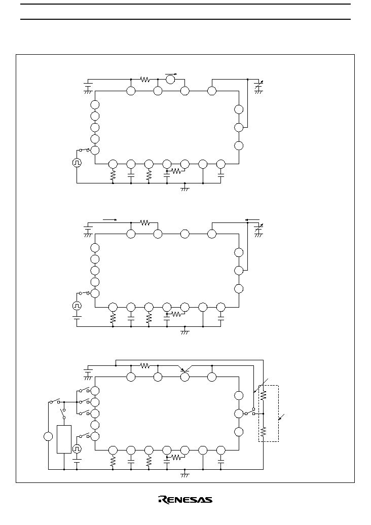
Test Circuits
STBY
NMI
RES
Voadj
P-RUN
Rf
Cf
R
R
C
R
R
T
GND
C
RES
STBYadj
NMIsns
NMIadj
V
CC
CS
CONT
Vout
A
Icont
390k
3300p
0.1
µ
180k
180k
1500p
Here, the Vout voltage is for a V
CC
of 12V, and Icont is monitored as
Vout is varied.
V
CC
f = 1kHz
duty = 50%
STBY
NMI
RES
Voadj
P-RUN
Rf
Cf
R
R
C
R
R
T
GND
C
RES
STBYadj
NMIsns
NMIadj
V
CC
CS
CONT
Vout
I
IN
390k
3300p
0.1
µ
180k
180k
1500p
V
CC
f = 1kHz
duty = 50%
STBY
NMI
RES
Voadj
P-RUN
Rf
Cf
R
R
C
R
R
T
GND
C
RES
STBYadj
NMIsns
NMIadj
V
CC
CS
CONT
Vout
390k
3300p
0.1
µ
180k
180k
1500p
V
CC
f = 1kHz
duty = 50%
Iout
Vout
Vout
*I
CC
= I
IN
+ Iout
∑
Vout test circuit
∑
I
CC
test circuit
∑
Test circuit for other parameters
Units: Resistors
Capacitors F
V
Frequency
counter
R2
390k
R1
13k
NMI
Vout
detection
NMI
V
CC
detection
HA16129AFPJ
HA16129AFPJ
HA16129AFPJ
HA16129AFPJ
17
System Circuit Examples
V
CC
STBY
P-RUN
Rf
Cf
GND
Voadj
OUTE
STBYadj
NMIadj
NMIsns
CONT
CS
V
OUT
C
RES
R
R
C
R
R
T
RES
NMI
1
2
3
4
5
6
7
8
9
10
20
19
18
17
16
15
14
13
12
11
HA16129AFPJ
0.2
+
200
µ
+
IGN
SW.
BATTERY
DS
STBY
RES
NMI
PORT
V
CC
(5 V)
Microprocessor
PORT
Load
To other power supplies
1500p
0.1
µ
3300p
180k
390k
180k
V
CC
STBY
P-RUN
Rf
Cf
GND
Voadj
OUTE
STBYadj
NMIadj
NMIsns
CONT
CS
V
OUT
C
RES
R
R
C
R
R
T
RES
NMI
1
2
3
4
5
6
7
8
9
10
20
19
18
17
16
15
14
13
12
11
HA16129AFPJ
0.2
+
200
µ
STBY
RES
NMI
PORT
V
CC
(5V)
Microprocessor
PORT
Load
1500p
0.1
µ
3300p
180k
390k
180k
+
IGN
SW.
BATTERY
D
S
To other power supplies
D
Z
Primary detection
Backup circuit
∑
Example of a basic system
∑
Example of a system using a backup circuit and a primary voltage monitoring circuit
D
S
:
D
Z
:
R2
R1
R3
R4
Q1
Q2
D1
R5
Schottky diode
Zener diode

HA16129AFPJ
18
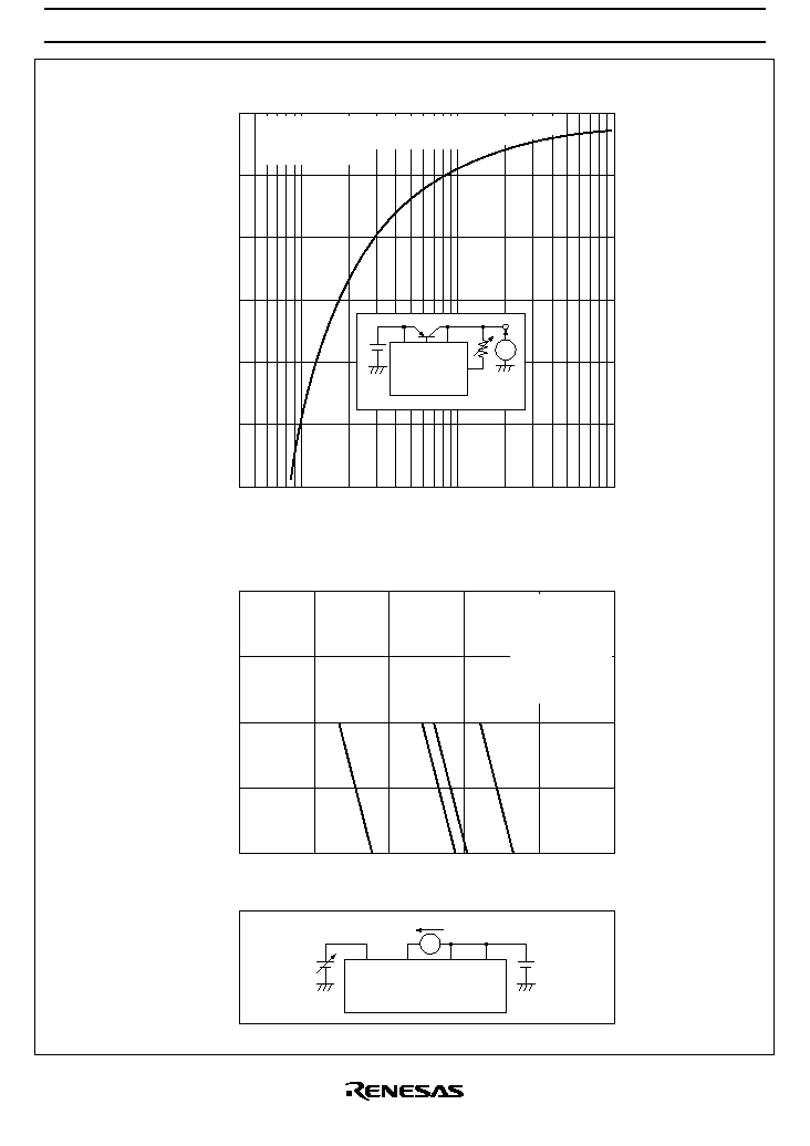
Operating Waveforms
100k
10k
100
10
20
30
Frequency vs. Duty Characteristics
40
50
60
70
80
90
100
Duty (%)
Frequency (Hz)
1k
Ta = 25
∞
C, C
R
= 0.1
µ
F, R
R
= 180k
,
R
T
= 390k
, Rf = 180k
, Cf = 3300pF
C
RES
= 1500pF
Runaway area
RES and OUTE
runaway detection
lines
OUTE normal
recovery line
Normal area
Pulse generator
V
OH
: 5V
V
OL
: 0V
RES
OUTE
Monitor
1000
100
10
1
10
Power On Time (t
ON
) vs. R
T
Resistance Characteristics
100
500
1000
R
T
Resistance (k
)
Power On Time (t
ON
) (ms)
50
Ta = 25
∞
C, V
CC
= 0
12V, Rf = 180k
,
Cf = 3300pF, C
RES
= 1500pF
5
500
50
C
R
= 0.47
µ
F
C
R
= 0.1
µ
F
C
R
= 0.033
µ
F

HA16129AFPJ
19
1000
500
50
10
Clock Off Time (toff) vs. R
R
Resistance Characteristics
Clock Off Time (toff) (ms)
100
Ta = 25
∞
C, Rf = 180k
, Cf = 3300pF,
C
RES
= 1500pF, R
T
= 390k
1000
100
10
1
10
Reset Pulse High Time (t
RH
) vs. R
R
Resistance Characteristics
100
500
1000
R
R
Resistance (k
)
Reset Pulse High Time (t
RH
) (ms)
50
Ta = 25
∞
C, Rf = 180k
, Cf = 3300pF,
R
T
= 390k
, C
RES
= 1500pF
5
500
50
C
R
= 0.47
µ
F
C
R
= 0.1
µ
F
C
R
= 0.033
µ
F
10
100
500
1000
R
R
Resistance (k
)
50
C
R
= 0.033
µ
F
C
R
= 0.1
µ
F
C
R
= 0.47
µ
F

HA16129AFPJ
20
Ta = 25
∞
C, Rf = 180k
, Cf = 3300pF,
R
T
= 390k
, C
RES
= 1500pF
10000
1000
100
10
10
100
500
1000
Rf Resistance (k
)
500
Ta = 25
∞
C, Cf = 3300pF, R
R
= 180k
,
R
T
= 390k
, C
R
= 0.1
µ
F
50
5000
50
C
RES
= 0.01
µ
F
C
RES
= 1500pF
C
RES
= 560pF
1000
100
10
1
10
100
500
1000
R
R
Resistance (k
)
50
5
500
50
RES
Delay Time and Recovery Time (tr) vs.
Rf Resistance Characteristics
RES
Delay Time and Recovery Time (tr) (
µ
s)
Reset Pulse Low Time (t
RL
) vs.
R
R
Resistance Characteristics
Reset Pulse Low Time (t
RL
) (ms)
C
R
= 0.033
µ
F
C
R
= 0.1
µ
F
C
R
= 0.47
µ
F

HA16129AFPJ
21
6.0
5.6
5.2
4.8
5000
∑
Roadj Resistance (to Ground) (k
)
5.4
Ta = 25
∞
C, V
CC
= 12V, Cf = 3300pF, Rf = 180k
,
C
R
= 0.1
µ
F, R
R
= 180k
, R
T
= 390k
, C
RES
= 1500pF
5.0
5.8
500
Output Voltage vs.
Roadj Resistance (to Ground) Characteristics
Output Voltage (V)
10000
1000
100
10
10
100
500
1000
Rf Resistance (k
)
500
Ta = 25
∞
C, Cf = 3300pF, R
R
= 180k
,
C
R
= 0.1
µ
F, R
T
= 390k
50
5000
50
C
RES
= 0.01
µ
F
C
RES
= 1500pF
C
RES
= 560pF
RES
Delay Time and Disable Time (t
RES
) vs.
Rf Resistance Characteristics
RES
Delay Time and Disable Time (t
RES
) (
µ
s)
100
1000
V
CC
Vout
Voadj
V
Roadj
HA16129AFPJ
22
Vout
V
CC
5.0
4.6
4.2
3.8
5 M
10 M
Roadj Resistance (to Vout) (k
)
4.4
Ta = 25
∞
C, V
CC
= 12V, Cf = 3300pF, Rf = 180k
,
C
R
= 0.1
µ
F, R
R
= 180k
, R
T
= 390k
,
C
RES
= 1500pF
4.0
4.8
500 k
Output Voltage vs.
Roadj Resistance (to Vout) Characteristics
Output Voltage Vout (V)
100 k
1 M
V
CC
Vout
Voadj
V
Roadj
CONT
A
CS
Vout
V
CC
12 V
I
CONT
5.00
5.02
4.96
4.94
4.98
4.92
40
0
20
10
30
I
CONT
Current (
µ
A)
Vout Voltage (V)
I
CONT
Current vs. Vout Voltage Characteristics
Vout Voltage (V)
Ta = 25
∞
C,
Cf = 3300pF,
Rf = 180k
,
C
R
= 0.1
µ
F,
R
R
= 180k
,
R
T
= 390k
,
C
RES
= 1500pF
HA16129AFPJ
23
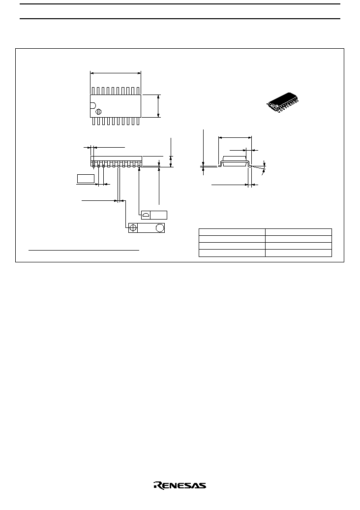
Package Dimensions
Hitachi Code
JEDEC
EIAJ
Mass (reference value)
FP-20DA
--
Conforms
0.31 g
Unit: mm
*Dimension including the plating thickness
Base material dimension
*0.42
±
0.08
0.12
0.15
M
20
10
1
*0.22
±
0.05
0.80 Max
11
12.6
5.5
2.20 Max
13 Max
0
∞
≠ 8
∞
0.70
±
0.20
+ 0.20
≠ 0.30
7.80
1.27
0.10
±
0.10
1.15
0.40
±
0.06
0.20
±
0.04

HA16129AFPJ
24
Cautions
1. Hitachi neither warrants nor grants licenses of any rights of Hitachi's or any third party's patent,
copyright, trademark, or other intellectual property rights for information contained in this document.
Hitachi bears no responsibility for problems that may arise with third party's rights, including
intellectual property rights, in connection with use of the information contained in this document.
2. Products and product specifications may be subject to change without notice. Confirm that you have
received the latest product standards or specifications before final design, purchase or use.
3. Hitachi makes every attempt to ensure that its products are of high quality and reliability. However,
contact Hitachi's sales office before using the product in an application that demands especially high
quality and reliability or where its failure or malfunction may directly threaten human life or cause risk
of bodily injury, such as aerospace, aeronautics, nuclear power, combustion control, transportation,
traffic, safety equipment or medical equipment for life support.
4. Design your application so that the product is used within the ranges guaranteed by Hitachi particularly
for maximum rating, operating supply voltage range, heat radiation characteristics, installation
conditions and other characteristics. Hitachi bears no responsibility for failure or damage when used
beyond the guaranteed ranges. Even within the guaranteed ranges, consider normally foreseeable
failure rates or failure modes in semiconductor devices and employ systemic measures such as fail-
safes, so that the equipment incorporating Hitachi product does not cause bodily injury, fire or other
consequential damage due to operation of the Hitachi product.
5. This product is not designed to be radiation resistant.
6. No one is permitted to reproduce or duplicate, in any form, the whole or part of this document without
written approval from Hitachi.
7. Contact Hitachi's sales office for any questions regarding this document or Hitachi semiconductor
products.
Hitachi, Ltd.
Semiconductor & Integrated Circuits.
Nippon Bldg., 2-6-2, Ohte-machi, Chiyoda-ku, Tokyo 100-0004, Japan
Tel: Tokyo (03) 3270-2111 Fax: (03) 3270-5109
Copyright © Hitachi, Ltd., 2001. All rights reserved. Printed in Japan.
Hitachi Asia Ltd.
Hitachi Tower
16 Collyer Quay #20-00,
Singapore 049318
Tel : <65>-538-6533/538-8577
Fax : <65>-538-6933/538-3877
URL : http://www.hitachi.com.sg
URL
NorthAmerica
: http://semiconductor.hitachi.com/
Europe
: http://www.hitachi-eu.com/hel/ecg
Asia
: http://sicapac.hitachi-asia.com
Japan
: http://www.hitachi.co.jp/Sicd/indx.htm
Hitachi Asia Ltd.
(Taipei Branch Office)
4/F, No. 167, Tun Hwa North Road,
Hung-Kuo Building,
Taipei (105), Taiwan
Tel : <886>-(2)-2718-3666
Fax : <886>-(2)-2718-8180
Telex : 23222 HAS-TP
URL : http://www.hitachi.com.tw
Hitachi Asia (Hong Kong) Ltd.
Group III (Electronic Components)
7/F., North Tower,
World Finance Centre,
Harbour City, Canton Road
Tsim Sha Tsui, Kowloon,
Hong Kong
Tel : <852>-(2)-735-9218
Fax : <852>-(2)-730-0281
URL : http://semiconductor.hitachi.com.hk
Hitachi Europe GmbH
Electronic Components Group
Dornacher Straþe 3
D-85622 Feldkirchen, Munich
Germany
Tel: <49> (89) 9 9180-0
Fax: <49> (89) 9 29 30 00
Hitachi Europe Ltd.
Electronic Components Group.
Whitebrook Park
Lower Cookham Road
Maidenhead
Berkshire SL6 8YA, United Kingdom
Tel: <44> (1628) 585000
Fax: <44> (1628) 585200
Hitachi Semiconductor
(America) Inc.
179 East Tasman Drive,
San Jose,CA 95134
Tel: <1> (408) 433-1990
Fax: <1>(408) 433-0223
For further information write to:
Colophon 3.0