 | –≠–ª–µ–∫—Ç—Ä–æ–Ω–Ω—ã–π –∫–æ–º–ø–æ–Ω–µ–Ω—Ç: I80134 | –°–∫–∞—á–∞—Ç—å:  PDF PDF  ZIP ZIP |

1
I80134
Product Data Sheet
Version 1.1 (December 1998)
Integrated Telecom Express, Inc.
I80134-ADSL Analog Front End
Features
!
Integrated Analog Front End (AFE) for
ADSL
!
8.8 MS/s ADC, 13 bits
!
Two 8.8 MS/s DACs, 12 bits
!
Low noise and distortion
!
4-bit digital interface
!
1V full scale input
!
16 dB programmable transmitter gain at
1 dB per step
!
31 dB programmable receive gain at 1
dB per step
!
Differential analog I/O
!
64-pin LQFP package
!
0.5 watts at 3.3V
!
3rd and 4th order tunable continuous
time low pass filters for channel filtering
for both TX and RX
General Description
ITeX's I80134 is a CMOS AFE designed for
Discrete MultiTone(DMT)-based, T1.413
Issue 2 compliant ADSL modems. The AFE
includes two 12-bit DACs and one 13-bit
ADC.
The I80134 has programmable low pass
filters for each of the three channels and
automatic gain control. The filter bank is
configured between the ATU-R and ATU-C
modes by the configuration pins. The
pipeline ADC architecture provides 13-bit
dynamic range and a signal bandwidth of
1.1 MHz. The AFE has a 0.5 watt power
consumption when it is in full operation.
The AFE also provides a power down mode
for standby function.
The I80134 can be used in both the ATU-R
and ATU-C side. The selection consists
mainly of a filter interchange between the
RX and TX path. The filters feature a
programmable cutoff frequency and use
automatic continuous time tuning to avoid a
time varying phase characteristic, which
could be of dramatic consequence for DMT
modems. The I80134 requires few external
components, and uses a 3.3V supply (a
separate 3.0V supply of the digital part is
possible).
An optional second TX path is also provided
for echo cancellation provision. The path
can be used in combination with an
additional adaptive filter (digital) to tune the
hybrid frequency response, in order to
reduce the power of the echoed TX signal.
On the digital interface, an alternative
modem with lower sampling rate (OSR=2;
4.4 MS/s) is provided, which allows support
of xDSL digital components operating at
different frequencies.
The I80134 is in a 64-pin LQFP package.

2
I80134
Product Data Sheet
Version 1.1 (December 1998)
Integrated Telecom Express, Inc.
Block Diagram
Introduction
The Receiver (RX) Subsystem
The DMT signal coming from the line to the
I80134 is first filtered by the two following
external filters:
!
POTS HP filter: Attenuation of speech
and POTS signaling
!
Channel filter: Attenuation of echo
signal to improve RX dynamic
An analog multiplexer allows the selection
between two input ports, which can be used
to select an attenuated (0,10 dB for ex.)
version of the signal in case of short loop or
large echo. The signal is amplified by a low
noise programmable gain stage (0-31 dB)
then low-pass filtered to avoid anti-aliasing,
and to ease further digital processing by
removing unwanted high frequency out-of-
band noise.
A 13 bit A/D converter samples the data at
8.832 MS/s (a 4.416Ms/s mode is also
possible), transforms the signal into a digital
representation, and sends it to the DMT
signal processor via the digital interface.
The Transmitter (TX/TXE)
Subsystem
The 12 bits of data at 8.832 MS/s (or 4.416
Ms/s) that comes from the DMT signal
processor through the digital interface is
transformed by a D/A converter into an
analog signal.
This signal is then filtered to decrease the
DMT sidelobes level and meet the ANSI
transmitter spectral response, as well as
reduce the out-of-band noise (which can be
echoed to the RX path) to an acceptable
level. The pre-driver buffers the signal for
the external line driver, and in case of a
CTRL/TST
INTERFACE
XTAL-DRIVER
VCXO
DAC
IV-REF
R-MOS-C
TUNING
DIGITAL INTERFACE
MUX
MUX
ADC
DAC
DACE
MUX
138kHz
SC1
138kHz
SC2
1.1MHz
HC1
1.1MHz
HC2
- +
+ -
+ -
- +
- +
+ -
13 bits
4 bits
12 bits
4 bits
4 bits
12 bits
TXEP
TXEN
TXP
TXN
RXP(0:1)
RXN(0:1)
AGCtxe
AGCtx
AGCrx
G=-15...0dB
step=1dB
G=-15...0dB
step=1dB
G=0...31
step=1dB

3
I80134
Product Data Sheet
Version 1.1 (December 1998)
Integrated Telecom Express, Inc.
short loop, provides an attenuation
provision (-15..0dB).
A second identical path is provided for echo
cancellation. If it is not used the TXE path
can be put in power down state.
The VCXO Control Subsystem
The VCXO is divided into an XTAL driver
and an auxiliary 8 bits DAC for timing
recovery.
The XTAL driver operates at 35.328 MHz
and provides an amplitude regulation
mechanism to avoid
temperature/supply/technology dependent
frequency pulling.
The DAC, which is driven by the CTRLIN pin
provides a current output with 8 bits
resolution that can be used to tune the
XTAL frequency with the help of external
components. The time constant of VCXO
tuning is set (via the CTRLIN interface) by
an internal switch and resistor network and
an external capacitor (on VCOC pin).
The Digital Interface Part
The digital part of the I80134 can be
divided in two parts:
The data interface converts the multiplexed
data from/to the DMT signal processor into
valid representation for the TX/TXE DAC
and RX ADC.
The control interface allows the board
processor to configure the I80134 paths
(RX/TX gains, filter band, etc.) or settings
(OSR, echo/vcodec enable, digital/analog
loopback, etc.).
Pin Diagram
64
63
62
61
60
59
58
57
56
55
54
53
52
51
50
48
17
18
19
20
21
22
23
24
25
26
27
28
29
30
31
32
47
46
45
44
43
42
41
40
39
38
37
36
35
34
33
49
1
2
3
4
5
6
7
8
9
10
11
12
13
14
15
16
TX1
TX0
TXE3
TXE2
TXE1
TXE0
CTRLIN
DVSS1
CLKM
CLNIB
CLWD
RX3
RX2
RX1
RX0
DVDD1
RXIP0
RXIN0
GC1
GC0
VCOC
GP2
AVDD6
AVDD5
TINN
TINP
AGND
TON
TOP
AVSS5
AVSS4
GP1
RXIN1
RXIP1
AVSS6
AVSS2
VCXO
IVCO
AVDD2
IREF
XTAL BYPASS
AVDD1
XTALI
XTALO
TX2
TX3
DVSS2
AVSS1
TXN
TXP
TXEN
TXEP
VREF
VRAN
AVD03
AVDD4
VRAP
AVSS3
GPO
TEST
DVDD2
PDOWN
LTNT
RSTIN
I80134
ANALOG FRONT END
4
I80134
Product Data Sheet
Version 1.1 (December 1998)
Integrated Telecom Express, Inc.
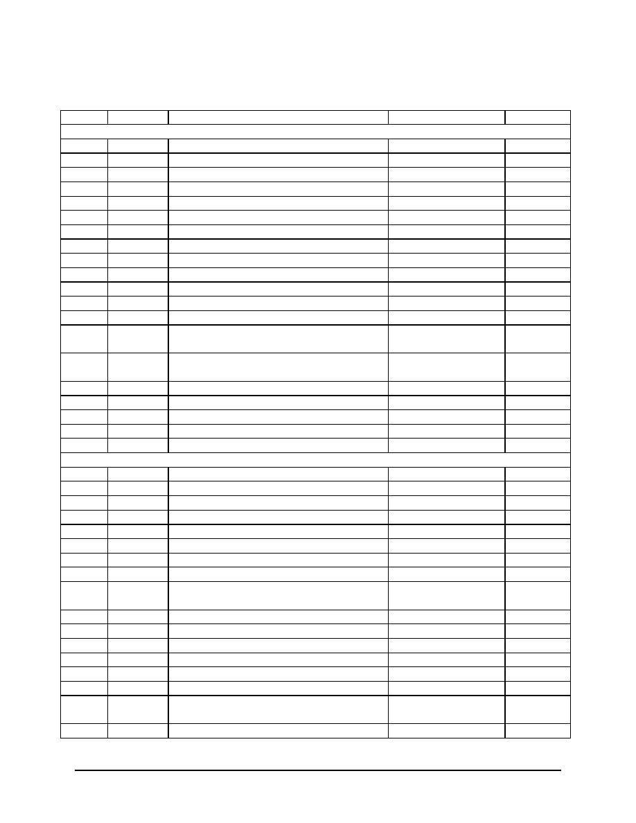
Pin Assignment and Description
Pin #
Name
Function
PCB Connection
Supply
Analog Interface
24
VRAP
positive voltage reference ADC
Decoupling network
AVDD3
25
VREF
ground reference ADC
Decoupling network
AVDD3
26
VRAN
negative voltage reference ADC
Decoupling network
AVDD3
29
TXEP
pre driver output for echo
LNA input
AVDD4
30
TXEN
pre driver output for echo
LNA input
AVDD4
31
TXP
pre driver output
Line driver input
AVDD4
32
TXN
pre driver output
Line driver input
AVDD4
38
AGND
virtual analog ground (AVDD/2=1.65V)
Decoupling network
AVDD5
44
VCOC
VCODAC time constant capacitor
VCODAC cap.
AVDD5
45
GC0
external gain control output LSB
AVDD5
46
GC1
external gain control output MSB
AVDD5
47
RXN0
analog receive negative input Gain 0
Echo filter output
AVDD5
48
RXP0
analog receive negative input Gain 0
Echo filter output
AVDD5
49
RXN1
analog receive negative input Gain 1
(most sensitive input)
Echo filter output
AVDD5
50
RXP1
analog receive negative input Gain 1
(most sensitive input)
Echo filter output
AVDD5
53
IREF
current reference TX DAC/DACE
Decoupling network
AVDD2
55
IVCO
current reference VCO DAC
VCO bias network
AVDD1
56
VCXO
VXCO control current
VCXO filter
AVDD1
59
XTALI
XTAL oscillator input pin
Crystal + varicap
AVDD1
60
XTALO
XTAL oscillator output pin
Crystal + varicap
AVDD1
Digital Interface
1
TX1
Digital transmit input, parallel data
DVDD2
2
TX0
Digital transmit input, parallel data
DVDD2
3
TXE3
Digital echo transmit input, parallel data
DVDD2
4
TXE2
Digital echo transmit input, parallel data
DVDD2
5
TXE1
Digital echo transmit input, parallel data
DVDD2
6
TXE0
Digital echo transmit input, parallel data
DVDD2
7
CTRLIN
Serial data input (settings)
sync interface
DVDD2
9
CLKM
Master clock output, f=35.328MHz
Load=CL<30pF
DVDD2
10
CLNIB
Nibble clock output, f=17.664MHz
(OSR=2) or ground (OSR=4)
Load=CL<30pF
DVDD2
11
CLWD
Word clock output, f=8.832/4.416MHz
Load=CL<30pF
DVDD2
12
RX3
Digital receive output, parallel data
Load=CL<30pF
DVDD2
13
RX2
Digital receive output, parallel data
Load=CL<30pF
DVDD2
14
RX1
Digital receive output, parallel data
Load=CL<30pF
15
RX0
Digital receive output, parallel data
Load=CL<30pF
DVDD2
18
PDOWN
Power down select, "1"=power down
Power down input
DVDD2
19
LTNT
NT(ATU-R)//LT(ATU-C) select pin,
NT=0/LT=1/test mode MSB
VDD in ATU-C mode
DVDD2
20
RESETN
Reset pin (active low)
RC-reset
DVDD2

5
I80134
Product Data Sheet
Version 1.1 (December 1998)
Integrated Telecom Express, Inc.
22
GP0
General purpose output 0 (on AVDD 1)
Echo filter output
AVDD
33
GP1
General purpose output 0 (on AVDD 1)
Echo filter output
AVDD
43
GP2
General purpose output 0 (on AVDD 1)
Echo filter output
AVDD
63
TX3
Digital transmit input, parallel data
Load=CL<30pF
DVDD2
64
TX2
Digital transmit input, parallel data
Load=CL<30pF
DVDD2
57
XTAL
bypass
DC coupling for XTAL
AVSS
AVDD1
Supply Voltages
8
DVSS1
DVSS
16
DVDD1
Digital I/O supply voltage
DVDD
17
DVDD2
Digital internal supply voltage
DVDD
23
AVSS3
AVSS
27
AVDD3
ADC supply voltage
AVDD
28
AVDD4
TX pre-drivers supply
AVSS
34
AVSS4
AVSS
35
AVSS5
AVSS
41
AVDD5
CT filter supply
AVDD
42
AVDD6
LNA supply
AVDD
51
AVSS6
AVSS
52
AVSS2
AVSS
54
AVDD2
DAC and support circuit
AVDD
58
AVDD1
XTAL oscillator supply voltage
AVDD
61
AVSS1
AVSS
62
DVSS2
DVSS
Package
The I80134 is in a 64-pin LQFP package.
©1998 ITeX
and Alcatel Alsthom. ITeX
is a trademark of Integrated Telecom Express, Inc. All other
trademarks are the sole property of their respective owners. Windows is a trademark of Microsoft
Corporation. ITeX's Standard Terms and Conditions, available upon request, apply to all sales. All
specifications are subject to change without notice.