Integrated Telecom Express, Inc.
1
I90188
Product Data Sheets
Version 1.3 (July 1999)
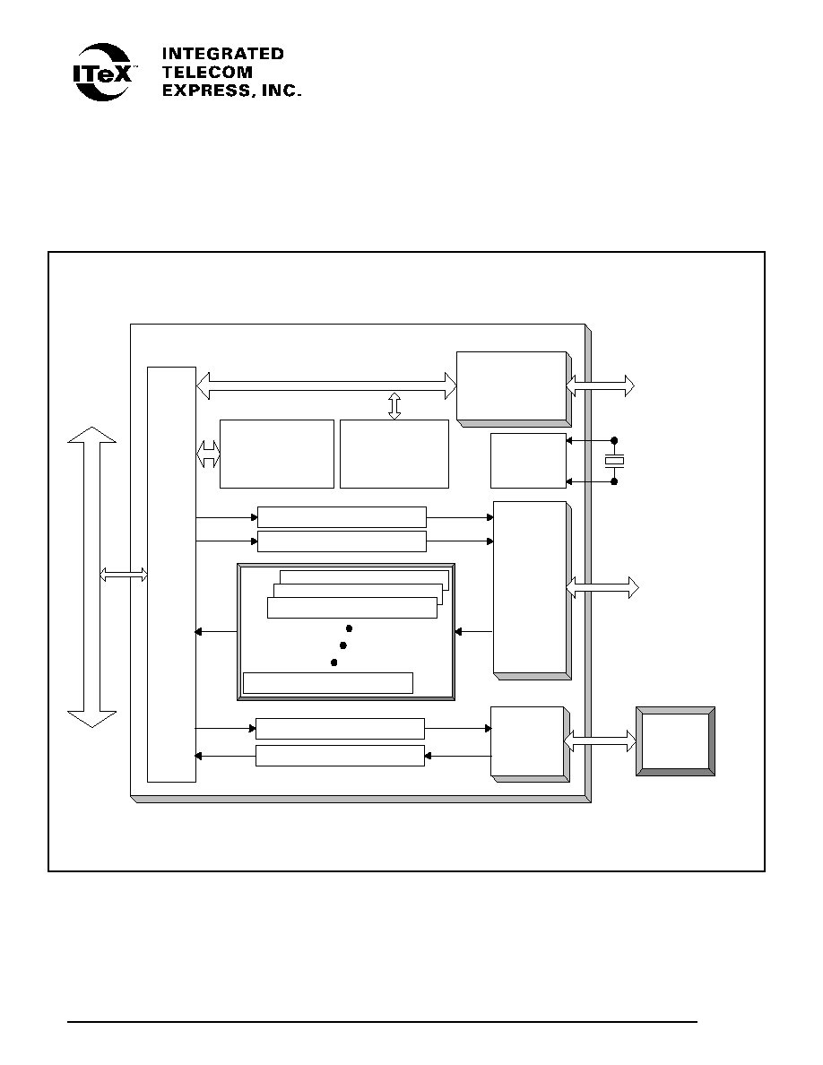
I90188-PCI/Utopia Interface Chip
Features
!
PCI Interface
-
Compliant with PCI Specification
v2.2
-
32-bit address/data bus
-
Bus frequency up to 33 MHz
-
Supports PCI master/slave device
-
Supports +3.3V or +5V PCI interface
!
Utopia Interface
-
Utopia level 1 and 2 support for D0
and D3 hot
-
8-bit data path
-
Full duplex
-
Cell-based-only
!
Supports T1.413 issue 2, ITU-T G.992.1
(G.dmt), and G.992.2 (G.lite) full rate
speed
!
ITeX I90135 interface
!
AC'97 Digital Controller
-
Compliant with AC'97 Component
Specification R2.1
-
Provides standard AC97-link
interface for AC'97 modem codec
-
Supports multiple sample rates
!
Eight general purpose I/O pins
-
Can be individually enabled or
disabled via software configuration
registers
-
Can be individually set as input or
output via software configuration
registers
!
+3.3V & +5V Power Supply
!
Package: 160-pin PQFP
General Description
The I90188 is a PCI to the Utopia interface
and an AC97-link digital bridge device. The
I90188 has an 8-bit full duplex cell-based-
only Utopia interface that connects to an
ADSL controller. The AC'97 digital controller
provides an Intel AC'97 v2.1 standard AC-
link interface. The device's 32-bit PCI
interface supports PCI slave/master devices,
and is PCI specification v.2.2 compliant.
The I90188 requires a single 25 MHz clock
frequency input and supports a 3.3V power
supply. The I90188 is available in a 160-pin
PQFP.
Integrated Telecom Express, Inc.
5
I90188
Product Data Sheets
Version 1.3 (July 1999)
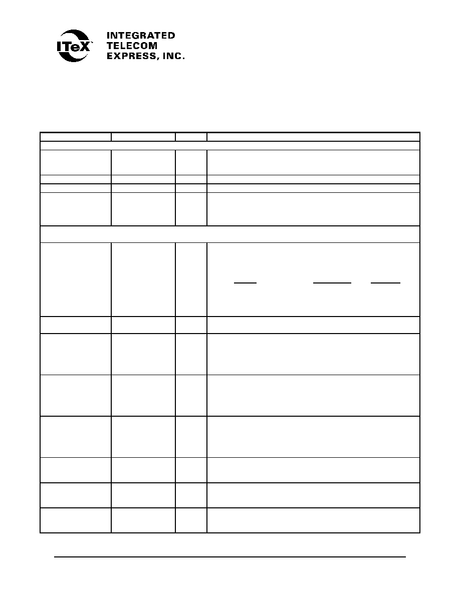
Pin Description
Symbol
Pin #
Type
Description
POWER SUPPLIES
V3
6, 16, 25, 35, 41,
57, 68, 80, 105,
121, 149, 160
PWR
+3.3V OR +5V Power Supply for PCI bus, I90135 and
Utopia Interface.
V35-AC97
138, 141
PWR
+3.3V OR +5V Power Supply for AC'97 (AC-LINK) Interface
V5
51, 87, 133, 135
PWR
+5V Power Supply for PUB core.
GND
1, 11, 20, 30, 40,
46, 63, 74, 81, 94,
112, 120, 126,
131, 143, 155
GND
Ground.
PCI BUS INTERFACE SIGNALS
AD[31:0]
150 - 154, 156 -
158, 3 - 5, 7 - 10,
12, 26 - 29, 31 -
34, 37 - 39,
42 - 45, 47.
DI/O
PCI Multiplexed Address / Data 31 - 0.
32-bit bi-directional address/data multiplexed lines AD31 is the MSB
and AD0 is the LSB. The direction of these pins are defined below:
PHASE
Bus Master
Target
Address Phase
Output
Input
Read Data Phase
Input
Output
Write Data Phase
Output
Input
C/BE[3:0]#
159, 13, 24, 36
DI/O
Command/Byte Enable 3 - 0 #.
Multiplexed bus command and byte enables.
DEVSEL#
18
DI/O
Device Select #.
When driven active low, the signal indicates the driving device has
decoded its address as the target of the current access. This pin
acts as an output pin when the I90188 (including ISA slave) is the
slave of PCI bus cycle transaction. Otherwise, it is an input pin.
TRDY#
17
DI/O
Target Ready #.
This signal indicates that the target of the current data phase of the
transaction is ready to be completed. This pin acts as an output pin
when the I90188 (including ISA slave) is the slave of the PCI bus
cycle transaction. Otherwise, it is an input pin.
IRDY#
15
DI/O
Initiator Ready #.
This signal indicates that the initiator is ready to complete the
current data phase of the transaction. This pin acts as an output pin
when the I90188 is the bus master of the PCI bus. Otherwise, it is
an input pin.
FRAME#
14
DI/O
FRAME #.
This signal is driven by the initiator to indicate the beginning and
duration of a PCI access.
IDSEL
2
DI
Initialization Device Select.
This signal is used as a chip select during configuration read and
write transactions.
PAR
23
DI/O
Parity
This signal is used for the even parity check on both AD[31:0] &
C/BE[3:0]# lines. The PAR input/output direction follows the