 | –≠–ª–µ–∫—Ç—Ä–æ–Ω–Ω—ã–π –∫–æ–º–ø–æ–Ω–µ–Ω—Ç: IAISM-AN1 | –°–∫–∞—á–∞—Ç—å:  PDF PDF  ZIP ZIP |
1
IA4420 Universal ISM Band
FSK Transceiver
D A T A S H E E T
W I R E L E S S
FEATURES
∑ Fully integrated (low BOM, easy design-in)
∑ No alignment required in production
∑ Fast-settling, programmable, high-resolution PLL synthesizer
∑ Fast frequency-hopping capability
∑ High bit rate (up to 115.2 kbps in digital mode and 256 kbps
in analog mode)
∑ Direct differential antenna input/output
∑ Integrated power amplifier
∑ Programmable TX frequency deviation (15 to 240 KHz)
∑ Programmable RX baseband bandwidth (67 to 400 kHz)
∑ Analog and digital RSSI outputs
∑ Automatic frequency control (AFC)
∑ Data quality detection (DQD)
∑ Internal data filtering and clock recovery
∑ RX synchron pattern recognition
∑ SPI compatible serial control interface
∑ Clock and reset signals for microcontroller
∑ 16 bit RX Data FIFO
∑ Two 8 bit TX data registers
∑ Low power duty cycle mode
∑ Standard 10 MHz crystal reference
∑ Wake-up timer
∑ 2.2 to 5.4 V supply voltage
∑ Low power consumption
∑ Low standby current (0.3
µ
A)
∑ Compact 16 pin TSSOP package
TYPICAL APPLICATIONS
∑ Remote control
∑ Home security and alarm
∑ Wireless keyboard/mouse and other PC peripherals
∑ Toy controls
∑ Remote keyless entry
∑ Tire pressure monitoring
∑ Telemetry
∑ Personal/patient data logging
∑ Remote automatic meter reading
See back page for ordering information.
DESCRIPTION
Integration's IA4420 is a single chip, low power, multi-channel FSK transceiver
designed for use in applications requiring FCC or ETSI conformance for unlicensed
use in the 315, 433, 868 and 915 MHz bands. The IA4420 transceiver is a part of
Integration's EZRadio
TM
product line, which produces a flexible, low cost, and
highly integrated solution that does not require production alignments. The chip
is a complete analog RF and baseband transceiver including a multi-band PLL
synthesizer with PA, LNA, I/Q down converter mixers, baseband filters and
amplifiers, and an I/Q demodulator. All required RF functions are integrated.
Only an external crystal and bypass filtering are needed for operation.
The IA4420 features a completely integrated PLL for easy RF design, and its rapid
settling time allows for fast frequency-hopping, bypassing multipath fading and
interference to achieve robust wireless links. The PLL's high resolution allows the
usage of multiple channels in any of the bands. The receiver baseband bandwidth
(BW) is programmable to accommodate various deviation, data rate and crystal
tolerance requirements. The transceiver employs the Zero-IF approach with I/Q
demodulation. Consequently, no external components (except crystal and
decoupling) are needed in most applications.
The IA4420 dramatically reduces the load on the microcontroller with the
integrated digital data processing features: data filtering, clock recovery, data
pattern recognition, integrated FIFO and TX data register. The automatic frequency
control (AFC) feature allows the use of a low accuracy (low cost) crystal. To
minimize the system cost, the IA4420 can provide a clock signal for the
microcontroller, avoiding the need for two crystals.
For low power applications, the IA4420 supports low duty cycle operation based
on the internal wake-up timer.
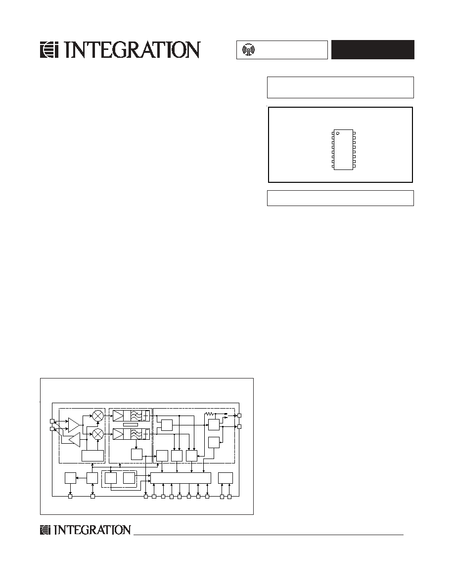
FUNCTIONAL BLOCK DIAGRAM
IA4420-DS Rev 1.4r 0705
www.integration.com
PRELIMINARY
IA4420
PIN ASSIGNMENT
revC and later
SDI
SCK
nSEL
SDO
nIRQ
FSK / DATA / nFFS
DCLK / CFIL / FFIT
CLK
nINT / VDI
ARSSI
VDD
VSS
RF1
RF2
nRES
XTL / REF
RF Parts
Low Power parts
Data processing units
BB Amp/Filt./Limiter
AMP
OC
AMP
OC
LNA
MIX
I
Q
MIX
Data Filt
CLK Rec
data
clk
DQD
COMP
RSSI
AFC
PLL & I/Q VCO
with cal.
Controller
Xosc
Self cal.
LBD
WTM
with cal.
CLK div
Bias
13
RF1
RF2 12
8
9
CLK
XTL /
REF
10
15
nINT /
VDI
ARSSI
2
3
4
5
11
SCK
nSEL
SDO
nIRQ
14
1
VSS
VDD
SDI
7
6
DCLK /
CFIL /
FFIT /
FSK /
DATA /
nFFS
FIFO
16
nRES
PA
I/Q
DEMOD
2
IA4420
DETAILED FEATURE-LEVEL DESCRIPTION
The IA4420 FSK transceiver is designed to cover the unlicensed
frequency bands at 315, 433, 868 and 915 MHz. The devices
facilitate compliance with FCC and ETSI requirements.
The receiver block employs the Zero-IF approach with I/Q
demodulation, allowing the use of a minimal number of external
components in a typical application. The IA4420 incorporates a
fully integrated multi-band PLL synthesizer, PA with antenna tuning,
an LNA with switchable gain, I/Q down converter mixers, baseband
filters and amplifiers, and an I/Q demodulator followed by a data
filter.
PLL
The programmable PLL synthesizer determines the operating
frequency, while preserving accuracy based on the on-chip crystal-
controlled reference oscillator. The PLL's high resolution allows the
usage of multiple channels in any of the bands.
The RF VCO in the PLL performs automatic calibration, which requires
only a few microseconds. Calibration always occurs when the
synthesizer starts. If temperature or supply voltage changes
significantly, VCO recalibration can be invoked easily. Recalibration
can be initiated at any time by switching the synthesizer off and
back on again.
The power amplifier has an open-collector differential output and
can directly drive a loop antenna with a programmable output power
level. An automatic antenna tuning circuit is built in to avoid costly
trimming procedures and the so-called "hand effect."
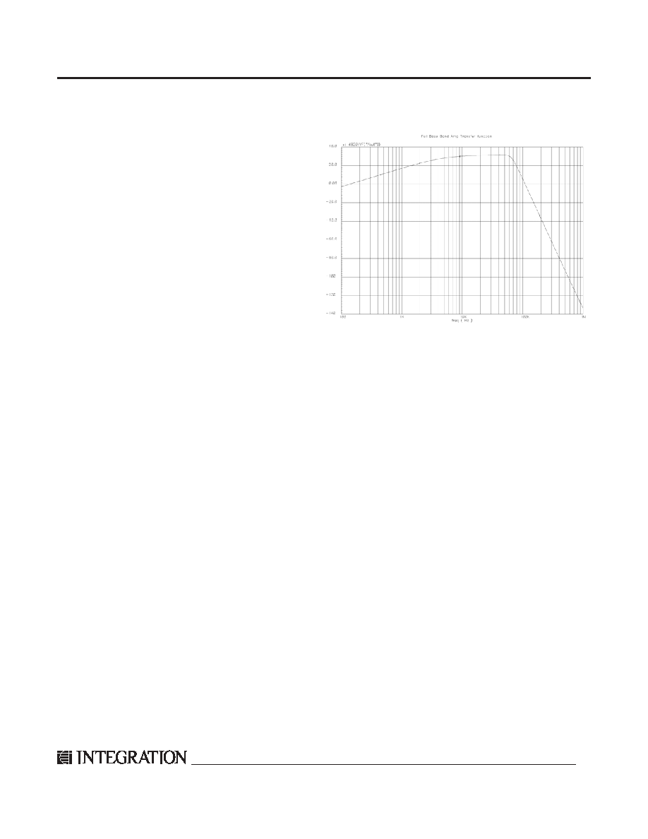
Baseband Filters
The receiver bandwidth is selectable by programming the bandwidth
(BW) of the baseband filters. This allows setting up the receiver
according to the characteristics of the signal to be received.
An appropriate bandwidth can be chosen to accommodate various
FSK deviation, data rate and crystal tolerance requirements. The
filter structure is 7th order Butterworth low-pass with 40 dB
suppression at 2*BW frequency. Offset cancellation is done by
using a high-pass filter with a cut-off frequency below 7 kHz.
LNA
The LNA has 250 Ohm input impedance, which functions well with
the proposed antennas (see: Application Notes available from
http://www.integration.com)
If the RF input of the chip is connected to 50 Ohm devices, an
external matching circuit is required to provide the correct matching
and to minimize the noise figure of the receiver.
The LNA gain can be selected (0, ≠6, ≠14, ≠20 dB relative to the
highest gain) according to RF signal strength. It can be useful in an
environment with strong interferers.
Data Filtering and Clock Recovery
Output data filtering can be completed by an external capacitor or by
using digital filtering according to the final application.
Analog operation:
Analog operation:
Analog operation:
Analog operation:
Analog operation: The filter is an RC type low-pass filter followed
by a Schmitt-trigger (St). The resistor (10 kOhm) and the St are
integrated on the chip. An (external) capacitor can be chosen according
to the actual bit rate. In this mode, the receiver can handle up to 256
kbps data rate. The FIFO can not be used in this mode and clock is
not provided for the demodulated data.
Digital operation:
Digital operation:
Digital operation:
Digital operation:
Digital operation: A digital filter is used with a clock frequency at
29 times the bit rate. In this mode there is a clock recovery circuit
(CR), which can provide synchronized clock to the data. Using this
clock the received data can fill a FIFO. The CR has three operation
modes: fast, slow, and automatic. In slow mode, its noise immunity
is very high, but it has slower settling time and requires more accurate
data timing than in fast mode. In automatic mode the CR automatically
changes between fast and slow mode. The CR starts in fast mode,
then after locking it automatically switches to slow mode
(Only the digital data filter and the clock recovery use the bit rate
clock. For analog operation, there is no need for setting the correct
bit rate.)
RF Power Amplifier (PA)
3
IA4420
Crystal Oscillator
The IA4420 has a single-pin crystal oscillator circuit, which provides
a 10 MHz reference signal for the PLL. To reduce external parts and
simplify design, the crystal load capacitor is internal and
programmable. Guidelines for selecting the appropriate crystal can
be found later in this datasheet.
The transceiver can supply the clock signal for the microcontroller;
so accurate timing is possible without the need for a second crystal.
Interface and Controller
An SPI compatible serial interface lets the user select the frequency
band, center frequency of the synthesizer, and the bandwidth of the
baseband signal path. Division ratio for the microcontroller clock,
wake-up timer period, and low supply voltage detector threshold are
also programmable. Any of these auxiliary functions can be disabled
when not needed. All parameters are set to default after power-on;
the programmed values are retained during sleep mode. The interface
supports the read-out of a status register, providing detailed
information about the status of the transceiver and the received
data.
The transmitter block is equipped with an 8 bit wide TX data register.
It is possible to write 8 bits into the register in burst mode and the
internal bit rate generator transmits the bits out with the predefined
rate.
It is also possible to store the received data bits into a FIFO register
and read them out in a buffered mode.
By using an integrated Automatic Frequency Control (AFC) feature,
the receiver can minimize the TX/RX offset in discrete steps, allowing
the use of:
∑
Inexpensive, low accuracy crystals
∑
Narrower receiver bandwidth (i.e. increased sensitivity)
∑
Higher data rate
AFC
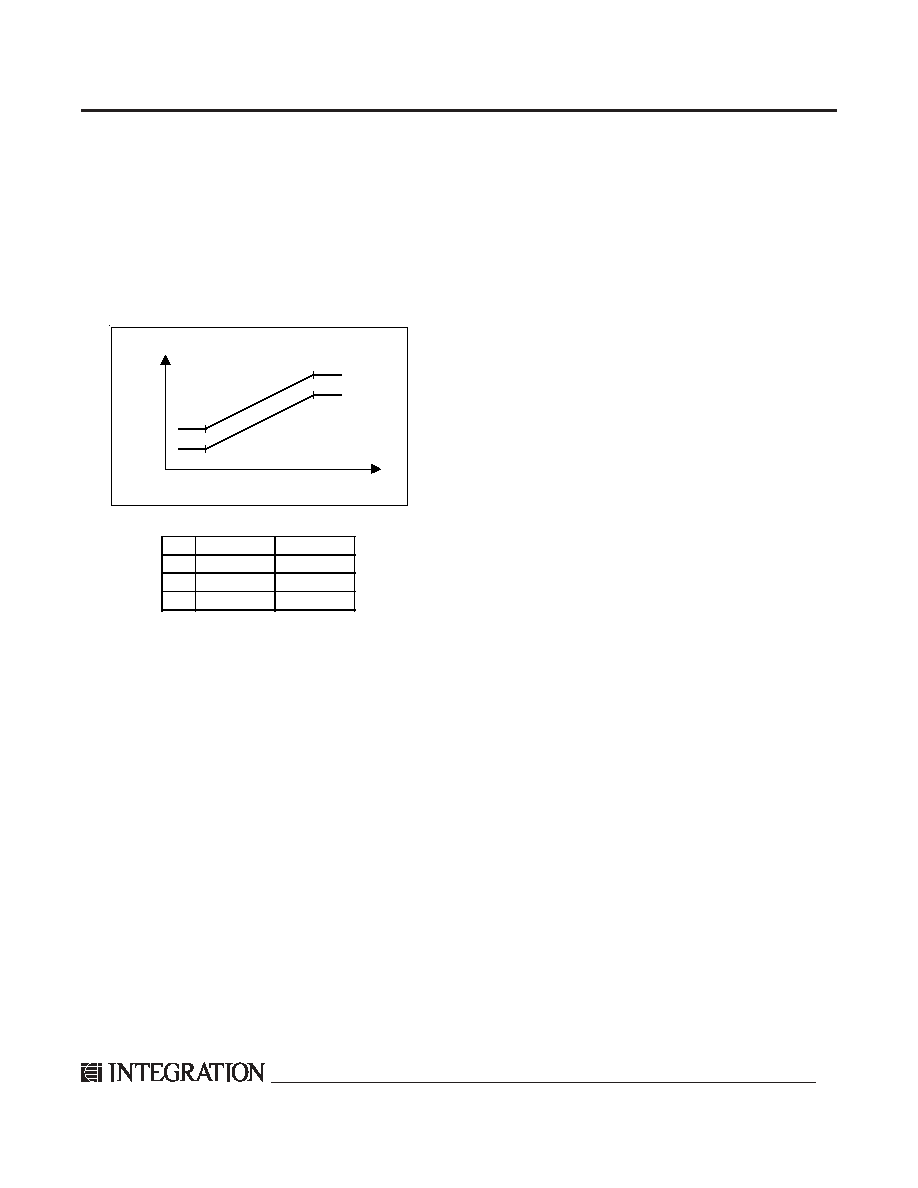
P1
-65 dBm
1300 mV
P2
-65 dBm
1000 mV
P3
-100 dBm
600 mV
P4
-100 dBm
300 mV
Input Power [dBm]
RSSI
voltage
[V]
P4
P2
P1
P3
Data Validity Blocks
R S S I
R S S I
R S S I
R S S I
R S S I
A digital RSSI output is provided to monitor the input signal level. It
goes high if the received signal strength exceeds a given
preprogrammed level. An analog RSSI signal is also available. The
RSSI settling time depends on the external filter capacitor. Pin 15 is
used as analog RSSI output. The digital RSSI can be can be monitored
by reading the status register.
Low Battery Voltage Detector
The low battery detector circuit monitors the supply voltage and
generates an interrupt if it falls below a programmable threshold
level. The detector circuit has 50 mV hysteresis.
Wake-Up Timer
The wake-up timer has very low current consumption (1.5 uA typical)
and can be programmed from 1 ms to several days with an accuracy
of ±5%.
It calibrates itself to the crystal oscillator at every startup, and then
at every 30 seconds. When the crystal oscillator is switched off, the
calibration circuit switches it back on only long enough for a quick
calibration (a few milliseconds) to facilitate accurate wake-up timing.
Event Handling
In order to minimize current consumption, the transceiver supports
different power saving modes. Active mode can be initiated by several
wake-up events (negative logical pulse on nINT input, wake-up timer
timeout, low supply voltage detection, on-chip FIFO filled up or
receiving a request through the serial interface).
If any wake-up event occurs, the wake-up logic generates an interrupt
signal, which can be used to wake up the microcontroller, effectively
reducing the period the microcontroller has to be active. The source
of the interrupt can be read out from the transceiver by the
microcontroller through the SDO pin.
D Q D
D Q D
D Q D
D Q D
D Q D
The Data Quality Detector is based on counting the spikes on the
unfiltered received data. For correct operation, the "DQD threshold"
parameter must be filled in by using the Data Filter Command.
Analog RSSI Voltage vs. RF Input Power
When the microcontroller turns the crystal oscillator off by clearing
the appropriate bit using the Configuration Setting Command, the
chip provides a fixed number (196) of further clock pulses ("clock
tail") for the microcontroller to let it go to idle or sleep mode.
4
IA4420
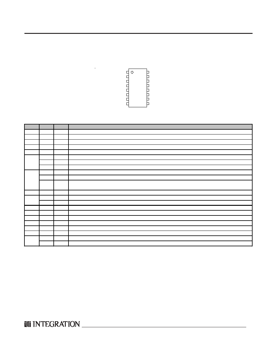
PACKAGE PIN DEFINITIONS
Pin type key: D=digital, A=analog, S=supply, I=input, O=output, IO=input/output
Note:
Note:
Note:
Note:
Note: The actual mode of the multipurpose pins (pin 6 and 7) is determined by the TX/RX data I/O settings of the
transceiver.
SDI
SCK
nSEL
SDO
nIRQ
FSK / DATA / nFFS
DCLK / CFIL / FFIT
CLK
nINT / VDI
ARSSI
VDD
VSS
RF1
RF2
nRES
XTL / REF
Pin
Name
Type
Function
1
SDI
DI
Data input of the serial control interface (SPI compatible)
2
SCK
DI
Clock input of the serial control interface
3
nSEL
DI
Chip select input of the serial control interface (active low)
4
SDO
DO
Serial data output with bus hold
5
nIRQ
DO
Interrupt request output (active low)
FSK
DI
Transmit FSK data input
DATA
DO
Received data output (FIFO not used)
nFFS
DI
FIFO select input (active low) In FIFO mode, when bit ef is set in Configuration Setting Command
DLCK
DO
Received data clock output (Digital filter used, FIFO not used)
CFIL
AIO
External data filter capacitor connection (Analog filter used)
FFIT
DO
FIFO interrupt (active high) Number of the bits in the RX FIFO that reach the preprogrammed limit
In FIFO mode, when bit ef is set in Configuration Setting Command
8
CLK
DO
Microcontroller clock output
XTL
AIO
Crystal connection (the other terminal of crystal to VSS) or external reference input
REF
AIO
External reference input. Use 33 pF series coupling capacitor
10
nRES
DIO
Open drain reset output with internal pull-up and input buffer (active low)
11
VSS
S
Ground reference voltage
12
RF2
AIO
RF differential signal input/output
13
RF1
AIO
RF differential signal input/output
14
VDD
S
Positive supply voltage
15
ARSSI
AO
Analog RSSI output
nINT
DI
Interrupt input (active low)
VDI
DO
Valid data indicator output
7
16
6
9
5
IA4420
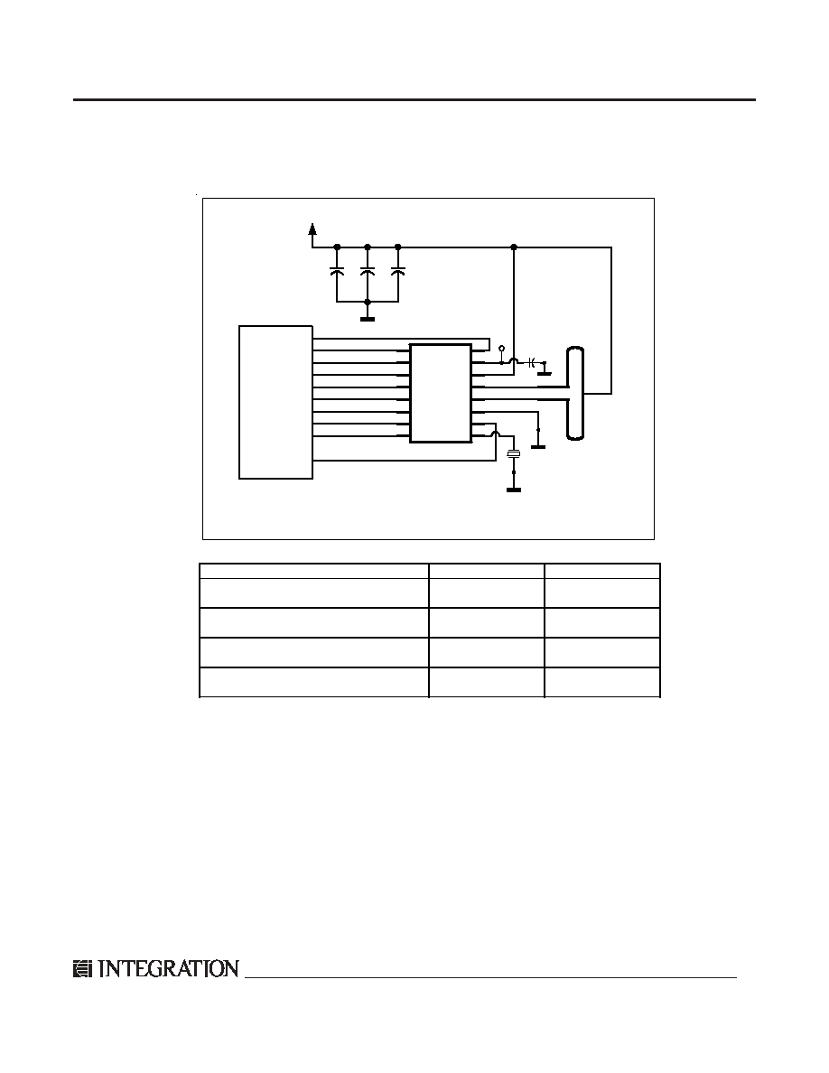
Typical Application
Typical application with FIFO usage
Pin 6
Pin 7
Transmit mode
el=0 in Configuration Setting Command
Transmit mode
el=1 in Configuration Setting Command
Receive mode
ef=0 in Configuration Setting Command
Receive mode
ef=1 in Configuration Setting Command
RX Data output
RX Data clock output
nFFS input
FFIT output
TX Data input
-
Connect to logic high
-
C2
100p
C3
10p
X1
10MHz
C1
1u
IA4420
1
3
4
2
5
7
6
8
9
10
11
12
13
14
15
16
VCC
SCK
SDO
nIRQ
P4
P3
P1
P2
SDI
CLKin
nSEL
nFFS
FFIT
nRES
PCB
Antenna
M
i
c
r
o
c
o
n
t
r
o
l
l
e
r
P5
P6
P7
nRES
C4
2.2n
P0
CLK
(optional)
TP
(optional)
(optional)
(optional)
(optional)
(optional)
VDI