IBM31T1100A
Integrated Infrared Transceiver Module
Highlights
x
IrDA 1.1, HP-SIR and Sharp ASK compliant
x
Supports IrDA data rates up to 4 Mbps
x
Low profile (height = 5.6 mm max.)
x
Minimum external components
x
On-chip LED protection circuit
x
Low power consumption
x
5 V Supply Voltage
x
Complete differential receiver design
x
Ambient light and noise rejection circuitry
x
Shutdown pin for power management
x
Programmable bandwidth control
x
Compatible with all major Super I/Os
General Description
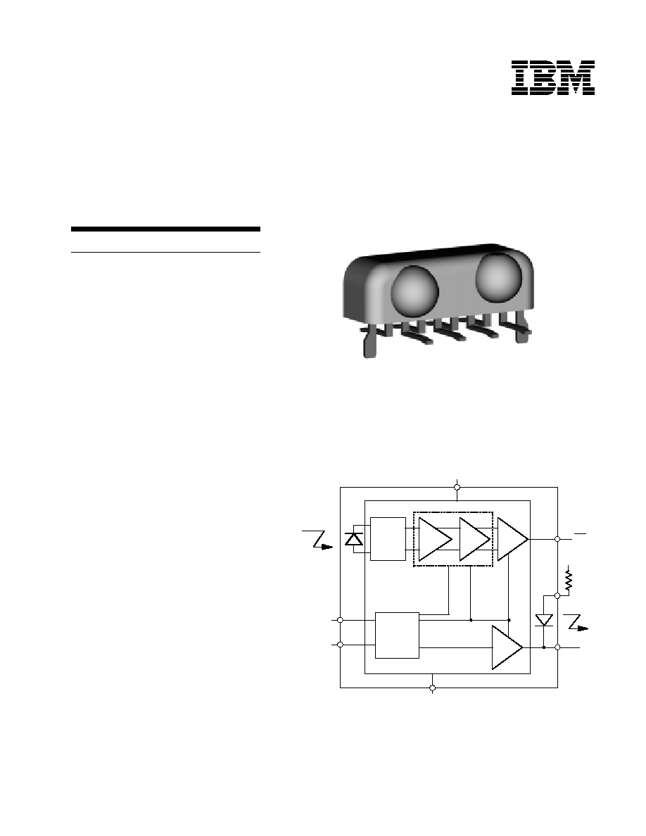
The IBM31T1100A is a multi-mode integrated
infrared (IR) transceiver module for data
communication systems. The transceiver supports
IrDA speeds up to 4 Mbps, HP-SIR and Sharp ASK
modes. Integrated into this tiny package is a
photodiode, LED and analog transceiver ASIC to
provide a total solution in a single package. A
current limiting resistor in series with the LED and
a Vcc bypass capacitor are the only external
components required to implement a complete
transceiver.
Package
GND
RX
1
8
2
TX
7
3
Vcc
6
4
Vcc
SD/BW
Driver
Comp
+
-
Noise
Rejection
Circuit
Amp
Driver
Control
logic
BW
SD
LEDC
LEDA
Block Diagram
IBM31T1100A
2
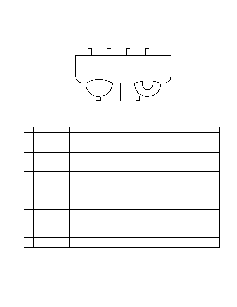
Pin Assignments and Descriptions
8
7
6
5
4
3
2
1
Photodiode
LED
LEDA
TX
SD/BW
NC
LEDC
RX
V
CC
GND
Pin
Pin Name
Description
I/O
Active
1
LEDC
Indicates the state of the internal LED cathode. Normally not connected.
O
Low
2
RX
Indicates received serial data. It is a push-pull CMOS driver capable of driving a
standard CMOS or TTL load. No external pull-up or pull-down resistor is required. May
switch indeterminately when the IBM31T1100A is transmitting.
O
Low
3
V
cc
Connect to +5 V power supply. Place a 1.0-10
PF ceramic bypass capacitor as close as
possible to this pin.
4
GND
Connect to ground of the power supply. A solid ground plane is recommended for proper
operation.
5
NC
This pin is reserved for special application use only. No signal should be connected to
this pin.
6
SD/BW
This CMOS input is used to put the IBM31T1100A in shutdown mode. Nominal supply
current draw in this mode is 35
PA versus 5 mA in normal mode. Together with the TX
input, this pin also sets the receiver bandwidth. If TX is low when SD/BW transitions
from high to low, the receiver bandwidth is optimized for operation up to 1.2 Mbps. If
TX is high when SD/BW transitions from high to low, the receiver bandwidth is
optimized for operation at 4 Mbps.
I
High
7
TX
Used to transmit serial data when SD/BW is low. This CMOS input controls the LED
driver. An on-chip protection circuit disables the LED driver if TX is high for more than
60
Psec. This pin is also used to program the bandwidth of the receiver. See SD/BW pin
description.
I
High
8
LEDA
Connect this input to Vcc through a resistor to set the proper LED current. Add an
external LED in series to increase output intensity if required.
I
Guide Pins
(not shown above)
Two through-hole guide pins provide mechanical stability during board mounting. They
also improve heat conduction when the part is in operation.
NOTE: The IBM31T1100A is pin and plug compatible with the Temic TFDS6000D.

IBM31T1100A
3
Electrical and Timing Specifications
Absolute Maximum Ratings
Symbol
Parameter
Min
Typ
Max
Unit
Condition
V
C C
Supply Voltage Range
- 0.5
6
V
P
D
Power Dissipation
450
mW
T
J
Junction Temperature
125
∞C
Storage Temperature Range
- 25
85
∞C
Soldering Temperature
240
∞C
See application notes
I
LED
LED Current
0.8
A
<2 µs, ton<10%
Voltage at Any Pin
- 0.5
Vcc+ 0.5
V
Recommended Operating Conditions
Symbol
Parameter
Min
Typ
Max
Unit
Condition
V
C C
Supply Voltage
4.5
5
5.5
V
T
A
Operating Temperature Range
0
70
∞C
DC Electrical Characteristics
T
A
= 0 - 70
qC, V
CC
= 5 V
r 10 %, unless otherwise specified
Symbol
Parameter
Min
Typ
Max
Unit
Condition
I
C C
Dynamic Supply Current
5
7
mA
SD = 0 V
I
C C
Standby Supply Current
35
100
uA
SD = V
CC
- 0.5, SC = NC
I
LED
Repetitive Pulsed LED Current
0.55
A
< 60 µs, ton d 25 %
V
OL
RX
Output Voltage Low @ I
OL
= 2.5 mA
0.3
0.5
V
V
OH
RX
Output Voltage High @ -I
OH
= 2.5 mA
V
CC
- 0.5
V
V
IL
Input Voltage Low (TX, SD/BW)
0
0.8
V
V
IH
Input Voltage High (TX)
3.0
V
V
IH
Input Voltage High (SD/BW)
V
CC
- 0.5
V
I
L
Input Leakage Current
-10
+10
uA
C
I
Input Capacitance
5
pF

IBM31T1100A
4
AC Electrical Characteristics
T
A
= 0 - 70
qC, V
CC
= 5 V
r 10 %, unless otherwise specified
Symbol
Parameter
Min
Typ
Max
Unit
Condition
t
R
RX
Rise Time
10
40
ns
R
LED
= 2.0 K
:, C = 50 pF
t
F
RX
Fall Time
10
40
ns
R
LED
= 2.0 K
:, C = 50 pF
t
S
TX Setup Time to SD/BW Low
200
ns
t
H
TX Hold Time from SD/BW Low
200
ns
t
PW
RX
Pulse Width
0.8
20
us
9.6 kbps
t
PW
RX
Pulse Width
100
500
ns
1.2 Mbps
t
PW
RX
Pulse Width
60
165
ns
4 Mbps
t
PW
RX
Pulse Width
185
290
ns
4 Mbps double pulse
t
D
Output Delay @ E
e
= 40 mW/cm
2
1
2
us
d 1.2 Mbps
t
L
Latency
120
us
t
R XEN
RX
Valid After Shutdown
60
us
t
DIS_ LED
LEDC Inactive After TX High
60
us
Optical Characteristics
T
A
= 0 - 70
qC, V
CC
= 5 V
r 10%, unless otherwise specified
Symbol
Parameter
Min
Typ
Max
Unit
Condition
E
emin
Minimum Detection Irradiance (SIR mode)
0.025
0.035
Wm
-2
9.6 - 115 kbps
E
emin
Minimum Detection Irradiance
0.035
0.05
Wm
-2
1.2 Mbps
E
emin
Minimum Detection Irradiance
0.07
0.08
Wm
-2
4 Mbps
E
emax
Maximum Detection Irradiance
5000
Wm
-2
All speeds
I
e
Output Radiant Intensity
100
140
320 (1)
mW/sr
Tx = High, SD = Low, R
LED
= 5.6
:
V
CC
=5.0,
D=0 q, D=r15 q, T
A
=25
qC
0.4
uW/sr
Tx=Low or SD=High, R
LED
=5.6
:
V
CC
=5.0,
D=0 q, D=r15 q, T
A
=25
qC
D
Output Radiant Intensity Half Angle
r24
q
O
P
Peak Wavelength
880
900
nm
Optical Overshoot
25
%
1.
Maximum intensity specified for class 1 operation of IEC 825-1
IBM31T1100A
5
I
F
o
r
wa
r
d
C
u
r
r
e
n
t
(
m
A
)
F
2.0
2.2
2.4
100
2.6
400
500
600
700
300
200
Max
Min
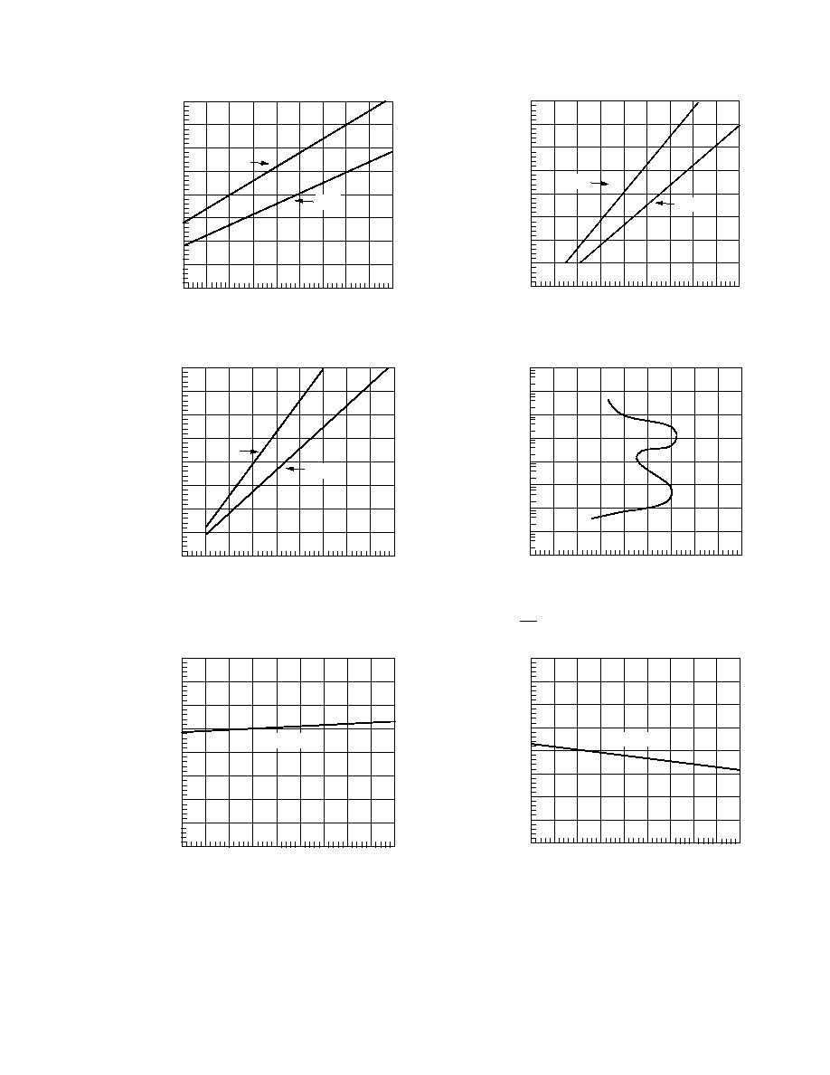
VLEDA Forward Voltage (V) - T = 25∞C
A
Figure 1. VLEDA to GND Voltage vs. peak LED current.
1.5
1.7
1.9
100
2.1
400
500
600
700
V LED Forward Voltage (V) - T = 25∞C
F
300
200
Max
I
L
E
D
F
o
rw
a
r
d
C
u
rre
n
t
(
m
A
)
F
A
Min
Figure 2. LED Forward Voltage vs. Current
0.2
0.4
0.6
25
Ou
tp
u
t
In
te
n
s
it
y
i
n
mW
/S
r
I Forward Current in Amperes
0.8
100
125
150
175
F
75
50
Typ
Min
Figure 3. Output Intensity vs. Current
50
100
150
0.001
I
n
p
u
t
I
rra
d
i
a
n
c
e
in
m
W
/
c
m
**2
RX pulse width in ns
200
1.0
10.0
100
1000
0.1
0.01
Figure 4.
RX
pulse width vs. Irradiance - 4 Mbps mode.
20
40
60
1.8
VL
ED
A
t
o
G
N
D
Vo
l
t
a
g
e
(
V
)
Temperature in ∞C
80
2.1
2.2
2.3
2.4
2.0
1.9
I =430mA
F
10
30
50
70
Figure 5. VLEDA to GND Voltage vs. Temperature.
20
40
60
25
Ou
tp
u
t
In
t
e
n
s
i
t
y
in
m
W
/S
r
Temperature in ∞C
80
100
125
150
175
75
50
I =430mA
F
10
30
50
70
Figure 6. Output Intensity vs. Temperature