
JA32050
8-Bit MCU,ADC,LCD Controller
Features
Operating Voltage: 2.4 V ~ 5.2V
Stand-by Current=2uA @VDD=3V
Operating Current = 2mA @ Fsys=2M
VDD=3V, ADC off
Built-in LCD driver: 4 COM * 20 SEG
LCD duty option: 1/3 duty or 1/4 duty
LCD bias option: 1/2 bias or 1/3 bias
R-Bias or C-Bias for LCD by mask option
RC oscillation for system clock (R external)
External 32.768 KHz crystal for RTC
Internal RC 32k for WDT or timer
Internal with dual slope ADC and 3 OP
amplifiers
Internal with an 8-bit I/O port dedicated for
ADC interface (Port A)
Normal 8-bit I/O port for general I/O (Port B)
with interrupt function
Internal with two16-bit timers (TMR0, TMR1)
Internal 8-bit WDT (watchdog timer)
R/F circuit available (PB0, PB1)
7K bytes of Program ROM
128 bytes of data RAM
STOP and HALT mode for power saving
Low battery detect
AVdd source current 20 mA
AVdd and Vdd separated
General Description
The JA32050 incorporates an 8-bit MCU, ADC,
LCD controller, timers, WDT, 8 programmable
general I/Os and R/F circuits inside. It is designed
for measuring application, especially suitable for
pressure related product such as manometer.
Block Diagram
Preliminary
19-1 Ver.0.0
TEL 886-3-5770755 FAX 886-3-5770756 E-mail sales@jaztek.com.tw Web-site www.jaztek.com.tw

JA32050
Pad Assignment
Pad Coordinates
Pad No.
Pad Name
X
Y
Pad No.
Pad Name
X
Y
1
SEG6
70.00
1866.18
13
OP1O
70.00
455.30
2
SEG5
70.00
1755.98
14
OP2O
70.00
327.40
3
SEG4
70.00
1645.78
15
OP2N
124.30
70.00
4
SEG3
70.00
1535.58
16
OP2P
234.50
70.00
5
SEG2
70.00
1425.38
17
OP3P
344.70
70.00
6
SEG1
70.00
1315.18
18
OP3N
454.90
70.00
7
SEG0
70.00
1204.98
19
OP3O
613.46
70.00
8
VDD
70.00
1085.47
20
REF1
779.94
70.00
9
VCC
70.00
969.06
21
VSS
890.14
70.00
10
VPP
70.00
849.00
22
RR
1000.34
70.00
11
OP1P
70.00
738.80
23
RC
1110.54
70.00
12
OP1N
70.00
628.60
24
CC
1262.95
70.00
Preliminary
19-2
Ver.0.0
TEL 886-3-5770755 FAX 886-3-5770756 E-mail sales@jaztek.com.tw Web-site www.jaztek.com.tw

JA32050
Pad No.
Pad Name
X
Y
Pad No.
Pad Name
X
Y
25
PB7
1419.58
70.00
42
COM2
2003.58
1619.08
26
PB6
1529.78
70.00
43
COM1
1974.44
1893.38
27
PB5
1639.98
70.00
44
COM0
1864.24
1893.38
28
PB4
1750.18
70.00
45
VLCD
1754.04
1893.38
29
PB3
1860.38
70.00
46
SEG19
1643.84
1893.38
30
PB2
1970.58
70.00
47
SEG18
1533.64
1893.38
31
PB1
2003.58
344.96
48
SEG17
1423.44
1893.38
32
PB0
2003.58
455.16
49
SEG16
1313.24
1893.38
33
SC
2003.58
588.93
50
SEG15
1203.04
1893.38
34
PDET
2003.58
724.48
51
SEG14
1092.84
1893.38
35
VDD
2003.58
834.68
52
SEG13
982.64
1893.38
36
OSCI
2003.58
944.88
53
SEG12
872.44
1893.38
37
VSS
2003.58
1055.08
54
SEG11
762.24
1893.38
38
RESB
2003.58
1165.28
55
SEG10
652.04
1893.38
39
XT1
2003.58
1275.48
56
SEG9
541.84
1893.38
40
XT2
2003.58
1385.68
57
SEG8
431.64
1893.38
41
COM3
2003.58
1508.88
58
SEG7
321.44
1893.38
Chip Size : 2073.58 x 1963.38( m)
2
Pin Descriptions
Pad No Pad Name
I/O
Description
1
SEG6
O
Segment 6
2
SEG5
O
Segment 5
3
SEG4
O
Segment 4
4
SEG3
O
Segment 3
5
SEG2
O
Segment 2
6
SEG1
O
Segment 1
7
SEG0
O
Segment 0
8
VDD
O
Positive power supply
9
AVDD
O Analog power supply (ON/Off by PA5)
10
VPP
I
Sensor power supply (SPWR)
11
OP1P
I
OP1 "+" input
12
OP1N
I
OP1 "-" input
13
OP1O
O OP1 output
14
OP2O
O OP2 output
15
OP2N
I
OP2 "-" input
16
OP2P
I
OP2 "+" input
17
OP3P
I
OP3 "+" input
18
OP3N
I
OP3 "-" input
19
OP3O
O OP3 output
20
REF1
O For reference voltage input
21
VSS
-- Negative power supply or GND
22
RR
I
2
nd
stage of internal amplifier
23
RC
I
2
nd
stage of OPA negative input end
24
CC
O 2
nd
stage of OPA output end
25
PB7
I/O PB I/O pin 7
Preliminary
19-3
Ver.0.0
TEL 886-3-5770755 FAX 886-3-5770756 E-mail sales@jaztek.com.tw Web-site www.jaztek.com.tw

JA32050
26
PB6
I/O PB I/O pin 6
27
PB5
I/O PB I/O pin 5
28
PB4
I/O PB I/O pin 4
29
PB3
I/O PB I/O pin 3
30
PB2
I/O PB I/O pin 2
31
PB1
I/O PB1: normal I/O pin 1 or RS, RF control pin
32
PB0
I/O PB0: normal I/O pin 0 or RS, RF control pin
33
SC
I/O R/F output pin, connected to MCU TMR pin
34
PDET
I
Low battery detect input
35
VDD
O Positive power supply
36
OSC
-- Oscillator generator I/O pins
37
VSS
-- Negative power supply or GND
38
RESB
I
System reset input, low active
39
X1
I
32.768k Hz crystal input
40
X2
I
32.768k Hz crystal input
41
COM3
O Common 3 of LCD
42
COM2
O Common 2 of LCD
43
COM1
O Common 1 of LCD
44
COM0
O Common 0 of LCD
45
VLCD
I
LCD panel bias voltage
46
SEG19
O
Segment 19, in C bias mode, this pin will be CAP2
47
SEG18
O
Segment 18, in C bias mode, this pin will be CAP1
48
SEG17
O
Segment 17, in C bias mode, this pin will be V30
49
SEG16
O
Segment 16, in C bias mode, this pin will be V15
50
SEG15
O
Segment 15
51
SEG14
O
Segment 14
52
SEG13
O
Segment 13
53
SEG12
O
Segment 12
54
SEG11
O
Segment 11
55
SEG10
O
Segment 10
56
SEG9
O
Segment 9
57
SEG8
O
Segment 8
58
SEG7
O
Segment 7
Electrical Characteristics
Test Condition
Symbol
Parameter
VDD
Condition
Min..
Typ.
Max.
Unit
VDD
Operating Voltage
2.2
3.0
5.2
V
IDD
Operating Current
3V
No Load,
Fsys=2MHz
2
3
mA
ISTB1
Standby Current
3V
Fsys OFF, 32K ON
3
5
A
ISTB2
Standby Current
3V
Fsys OFF, 32K
OFF
1
3
A
RPH
Pull high resistor
3V
PB0 � PB7
100
k
IOH1
PB0, PB1 Source
Current
3V
VOH1=2.7V
20
30
mA
IOL1
PB0, PB1 Sink Current
3V
VOL1=0.3V
20
30
mA
IOH2
PB2 PB7 Source
Current
3V
VOH1=2.7V
1
3
mA
IOL2
PB2 PB7 Sink current
3V
VOL2=0.3V
1
3
mA
IOL3
SC sink current
3V
VOL3=0.3V
20
30
mA
Preliminary
19-4
Ver.0.0
TEL 886-3-5770755 FAX 886-3-5770756 E-mail sales@jaztek.com.tw Web-site www.jaztek.com.tw
JA32050
IOL4
LCD COM, SEG Sink
Current
3V
VOL4=0.3V
80
150
A
IOH3
LCD COM, SEG
Source Current
3V
VOH2=2.7V
50
80
A
MCU Function Description
JA32050 contains a 6502 based 8-bit Micro-Controller Unit (MCU) with Program ROM, Special register, user
data RAM and two 16-bit Timers inside. This chip also provides multi external interrupt pins (I/O Port B) and
Low Voltage Detector (LVD) function.
Memory
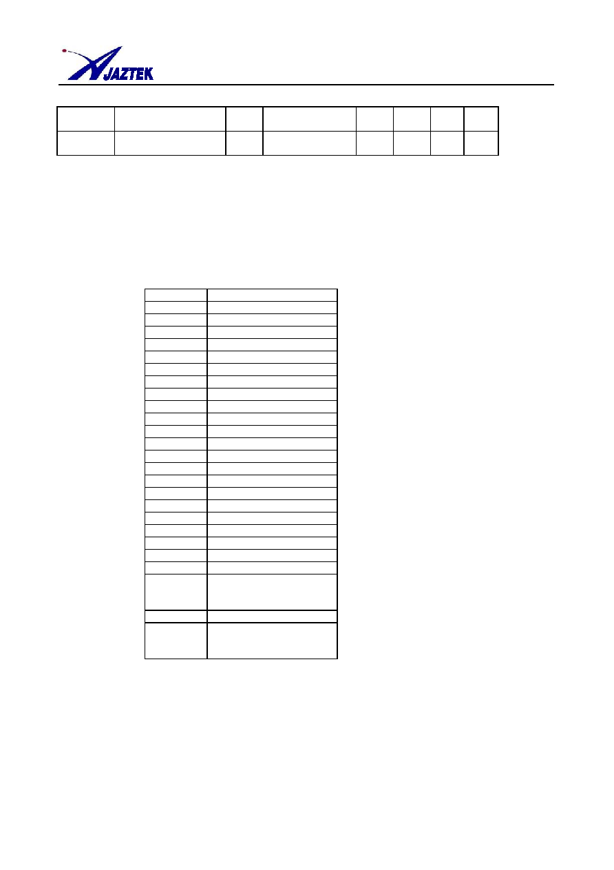
Memory Mapping
Address
Definition
00h
POWERC (R/W)
01h
INTC (R/W)
02h
INTF (R/W)
03h
WDTCLR (W)
04h
WDTC (R/W)
05h
TMR0H (R/W)
06h
TMR0L (R/W)
07h
TMR0C (R/W)
08h
TMR1H (R/W)
09h
TMR1L (R/W)
0Ah
TMR1C (R/W)
0Bh
PA (R/W)
0Ch
PAC (R/W)
0Dh
PAR (R/W)
0Eh
PB (R/W)
0Fh
PBC (R/W)
10h
PBR (R/W)
11h-1Fh
Reserved
21h
CON0
22h
Reserved
23h
LCD0
24h
LCD1
80h
~
FFh
General purpose
Data Memory & Stack
200h ~ 213h
LCD data RAM
E400h
~
FFFFh
User Program
Data RAM
Total 128 bytes of Data RAM (including the stack) are available from $80h to $FFh.
Program ROM
Total 7K bytes of user ROM located from $E400h to $FFFFh are available.
Reset & Interrupt Vector
The reset vector is located at $FFFCh, and interrupt vector followed.
Stack Pointer
The stack pointer is set from $FFh after power on.
Preliminary
19-5
Ver.0.0
TEL 886-3-5770755 FAX 886-3-5770756 E-mail sales@jaztek.com.tw Web-site www.jaztek.com.tw