
Silicon Video, Inc. 2003
Product DATASHEET PDS0001 REV. N Subject to change without notice. Page 1 of 14
LIS-1024 High Performance Linear CMOS Image Sensor
The LIS-1024 image sensor is a high performance, very low noise linear image sensor designed for a wide
variety of applications including:
∑
Spectroscopy
∑
Bar Code Reading
∑
Edge Detection
∑
Contact Scanning
∑
Optical Character Recognition
∑
Encoding
∑
Position Detection
∑
And more.......
Description
The LIS-1024 Image Sensor consist of an array of ultra low dark current photo-diode pixels with performance
exceeding most Charge-Coupled Devices (CCD's). The device has multiple read out modes, including: Non-
Destructive, Dynamic Pixel ResetTM (DPR), and Frame Reset.
The Non-destructive mode enables extremely low noise measurements (approaching a single electron) through
the use of signal averaging, enabling the system to achieve near single electron noise performance, making the
device ideally suited for any high performance measurement application. In DPR mode, each pixel is reset as it
is read, ensuring each pixel integrates for the same amount of time. Other reset modes are also provided to give
exceptional control over exposure time and pixel read out. The Sensor also operates over an extended power
supply range of 2.8-5.0 VDC.
Operation is simplified by on-chip logic. The only external signals required are a clock with a frequency equal to
the desired pixel read rate, a reset mode selection, and an external reset to initiate read-out when running
asynchronously.
The LIS-1024 is supplied in a 16-pin LCC package as shown above.
P/N: LIS-1024D-LG
16-pin LCC package
Silicon Video Inc.
P.O. Box 4902, Ithaca, NY 14852-4902,
.
TEL: 607.756.5200
,
FAX: 607.756.5319
www.siliconvideo.biz
,
sales@siliconvideo.biz
Silicon Video, Inc. 2003
Product DATASHEET PDS0001 REV. N Subject to change without notice. Page 2 of 14
Key Features
∑ Low Cost
∑ Single Supply Operation
∑ Multiple read out modes
∑ Ultra Low Noise ( 1 e
-
via signal averaging)
∑ High Signal to Noise
∑ Non-Destructive read capable
∑ 1.0 kHz to 20.0 MHz Operation
∑ Very Low Dark Current
∑ Completely integrated Timing and Control
∑ Replaces CCD systems, not just the sensor
∑ 1 x 1024 pixel resolution
∑ 7.8 micron pitch x 125 microns tall
∑ Photo-active area: 7.988 mm x 125 microns
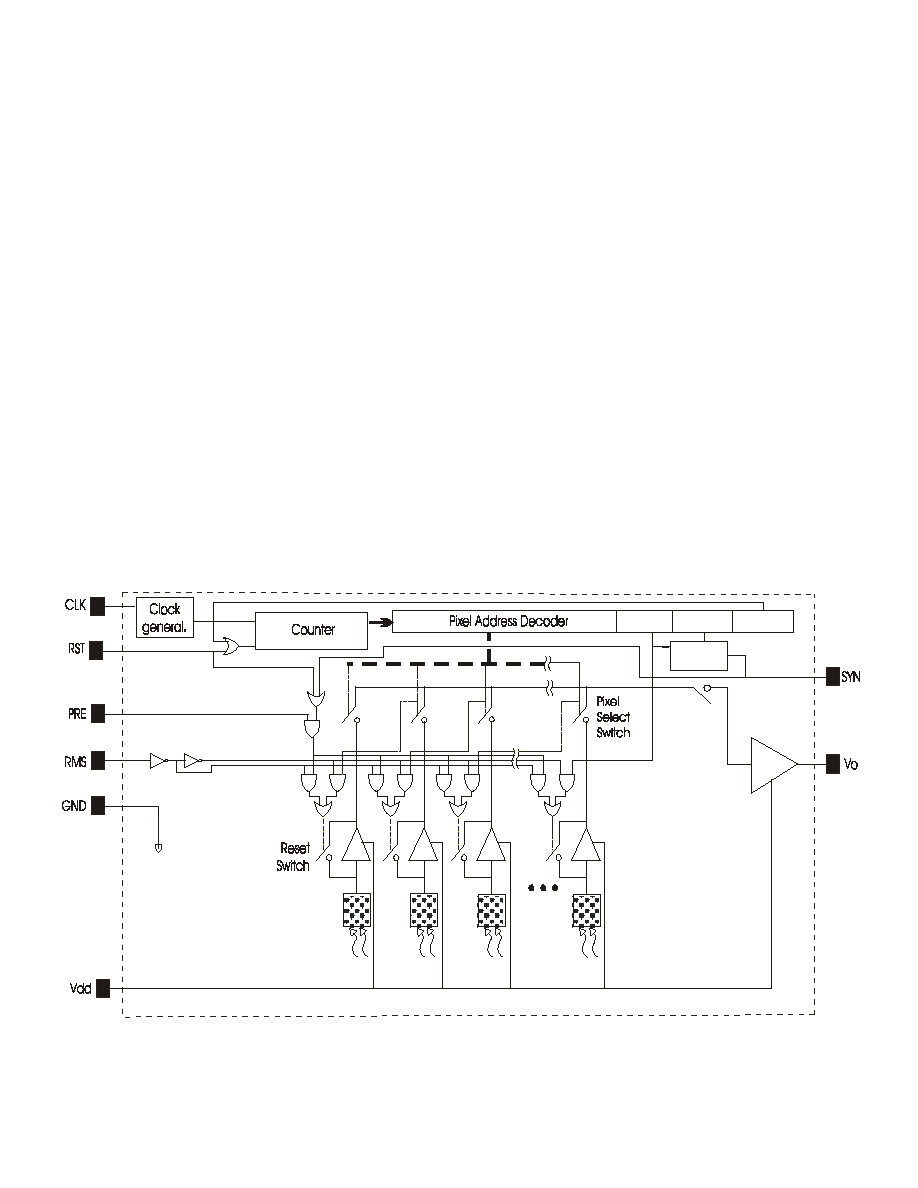
Functional Block Diagram
1 0 2 6
1 0 2 8
1 0 2 9
R
S/R F F
R
S
Pixe l 1
Pixe l 2
Pixe l 3
Pixe l X X X
Q

Silicon Video, Inc. 2003
Product DATASHEET PDS0001 REV. N Subject to change without notice. Page 3 of 14
Absolute maximum ratings, T
A
= 25
∞
C unless otherwise noted, see Note 1, below.
Supply voltage range, V
DD
------------------------------------------------
0
V to 5.25 V
Digital input current range, I ---------------------------------------------
≠20 mA to 20 mA
Input signal overshoot ---------------------------------------------------- Vdd +0.250v (High), Vss ≠
0.25v (Low)
Operating free-air temperature range, T
A --------------------------------
0∞C to 50∞C
Storage temperature range ------------------------------------------------ ≠20∞C to 85∞C
Humidity range, Rh -------------------------------------------------------- 0-85%, non-condensing
Lead temperature 1.5 mm (0.06 inch) from case for 10 seconds----- 225∞C
Exceeding the ranges specified under "absolute maximum ratings" can damage the device. The values given are for stress
ratings only. Operation of the device at conditions other than those indicated under "recommended operating conditions" is not
implied. Exposing the device to absolute maximum rated conditions for extended periods may affect device reliability and
performance.
NOTES: 1. Voltage values are with respect to the device GND terminal.
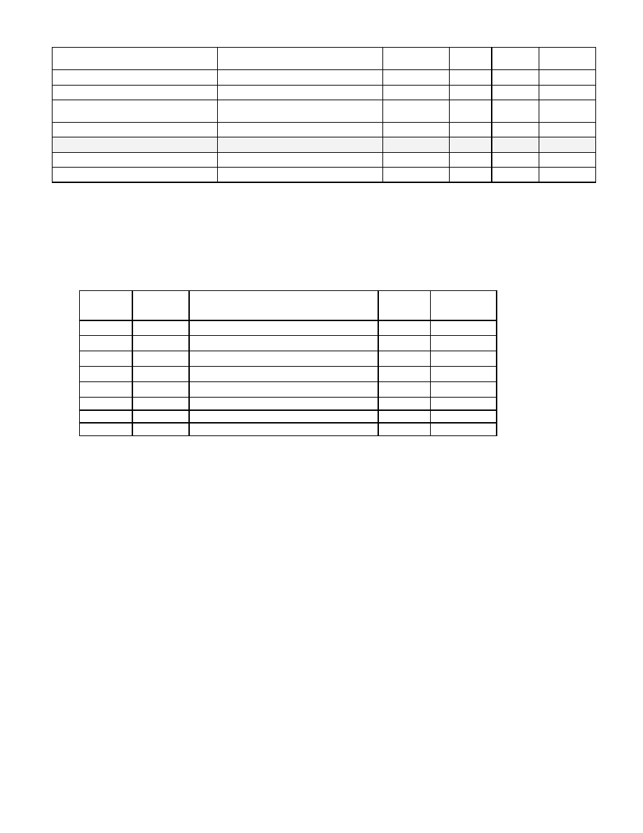
LIS-1024 Electrical Characteristics/Operating Conditions
(@T
A
= 25
∞C, VDD= I/OLEVEL = 5.0VDC, CLK
IN
= 1 MHz, unless otherwise specified)
Parameter
Conditions
Min
Typ
Max
Units
Digital Signals
Input High Logic Level (V
iH
) Vdd≠0.6V
V
Input Low Logic Level (V
iL
)
0.6
V
Digital Out load current (I
out
)
1.0
mA
Input Clock Freq. (CLK
IN
)
Pixel Read Rate (ERC) = CLK
IN
1.0 1,000
20,000
MHz
Input Clock Duty Cycle
40
60
%
t pcdly - Clk to 1
st
pixel
Rising edge of clock
2
ns
t rsh - RST Set Up & Hold
Spec in # of Clock Cycles See Note 2
3
CLK
IN
t sdly - Sync Out to Clk Dly.
Rising & falling edge of Sync out to
rising edge of clock
1
120
ns
t spix - Sync out to 1
st
pixel
Falling edge of SYN.
Spec in # of Clock Cycles
2
CLK
IN
DC
Supply Voltage (Vdd)
@ Supply voltages less than Sat
Voltage, VO is clipped by supply, no
load applied.
2.80 5.0 V
Supply Current
Including Load Resistor
8 18
50 ma
Video Output
See Note 1
Video Out (VO) ≠ Ext. Load
@ Supply voltages less than Saturation
Voltage, VO is clipped by supply, no
load applied.
330
10k
Ohms
Output Voltage @ Saturation
2.8
3.3
4.0
V
Output Voltage @ Dark
0.64
0.74
0.84
V
Electro-optical
See Note 1
Pixel FPN - PRNU
Non-Uniformity 50% Sat
±0.3
%
Total
Pixel FPN - DSNU
Non-Uniformity Dark
±0.3
%
Total
Linearity
Pixel avg. from 5% - 75% Saturation
1.0
%
SAT
Well Capacity (Full Well)
8.0
Me-
Silicon Video, Inc. 2003
Product DATASHEET PDS0001 REV. N Subject to change without notice. Page 4 of 14
Sensitivity
From 5% - 75% Saturation. Unloaded
video, values typical and may vary.
0.32
µv/e-
Quantum Efficiency
675nm
60
%
Output Due To Dark Current
At 24 ∞C
2 19
38
mV/s
Signal/Noise (RMS)
Temporal RMS noise @ 1 MHz erc and
500 KHz video bandwidth filter applied.
>84
db
Spectral Response Range
350
1100
nm
Environmental
Relative Humidity Range
0
85
%
Operating Temperature Range
0
25
50
∞C
Note 1:
Specs. given at pixel read rates of 1 MHz. At higher read rates, MTF and S/N begin to degrade. End pixels response
may vary from nominal array characteristics. S/N values are typical and may vary. Higher S/N ratios obtainable with
lower clock speed and bandwidths.
Note 2: RST is specified to be initiated for 3 CLK
IN
cycles to insure proper reset of pixels
.
Shorter pulse widths will
reset the internal timing, but may not fully reset pixels.
SIGNAL DESCRIPTION & PACKAGE PINOUT
Signal I/O
type
Definition
8 Pin
DIP
16 Pad
LCC
GND -----
Ground
Reference.
1
1
CLK
Input
Clock
2
3
PRE
Input
Pixel Reset Enable
3
5
RMS Input
Reset Mode Select
4
7
RST
Input
External Reset/Start pixel read
5
10
VO Output
Video
Output
6
12
SYN Output
Sync
Output
7
14
VDD Input
Supply
Voltage
8
16
OPERATION AND TIMING
The device offers multiple modes of operation including:
∑ Dynamic Pixel ResetTM (DPR) Mode: Each pixel is reset after reading,
∑ Dynamic Pixel ResetTM (DPR) Non-Destructive Mode: Each pixel is allowed to integrate even after
reading,
∑ Frame Mode Destructive Read: All pixels are reset all at once
∑ Frame Mode Non-Destructive Read: All pixels originally reset at once and allowed to integrate after
reading.
Example timing diagrams are given below. The user determines mode of operation by selecting logic levels for the
PRE (Pixel Reset Enable) pin and the RMS (Reset Mode Select) pin. The device requires a clock frequency equal to
the desired pixel read rate. In frame mode, a read cycle is initiated by the internal reset node or by pulsing the RST
pin. See the Reset Mode Truth Table for all modes of operation.
In all modes, the end of each frame is identified with a pulse being output on the SYN pin. This SYN pulse will go
high on the rising edge of the 1026 clock cycle count for that frame. The SYN pulse goes low on the rising edge of
the 1028 clock count. The Sync Output (SYN) pin goes high for 2 clock counts. The internal counter is reset on the
rising edge of the 1029 clock count.
Mode inputs RMS & PRE may be initiated asynchronously. It is recommended that changes to mode inputs be made
between counts 1025 (after last pixel) and 1028 (falling edge of sync out). One full frame of video may be required
to achieve valid data, dependant on when PRE, and RMS are initiated.

Silicon Video, Inc. 2003
Product DATASHEET PDS0001 REV. N Subject to change without notice. Page 5 of 14
RST pin is used for external reset. RST may be initiated asynchronously One full frame of video may be required to
achieve valid data, dependant on when RST is initiated in DPR modes. Active high, RST resets the internal counter,
and resets pixels when PRE is held low. Initiating RST pin interrupts SYN output.
NOTES TO TIMING DIAGRAMS
1. Clock duty cycle should be 40% to 60%.
2. 1024 Clock cycles for the number of pixels to read, starting at the first pixel.
3. t int represents integration time.
4. t cnt represents clock cycle count
5. t
rpix
represents time between falling edge of RST and 1
st
rising edge of CLK
IN
6. RST pulse always resets internal counter, thus next pixel output is the first pixel.
Figure 1: LIS-1024 Free Running Timing Setup
CLK
SYN
PRE & RMS
VO
Mode Setup
Internal Reset
Pixel 1
t cnt:
1024
1025
1026
1027
1028
1029
1
t sdly
t spix
Pixel 2
Pixel
1024
Pixel
1023
t pcdly
2
1023
Reccomended
Integration Begins
Figure 2: LIS-1024 External Reset Timing Setup (PRE Held High)
CLK
RST
VO
Pixel 1
t cnt:
N +1
N +2
N +3
N +4
N +6
1
Asynchronous Reset
Pixel 2
Pixel N +1
Pixel N
t pcdly
2
N
N +5
Pixel N +2
1st Pixel Read out
on next Rising Edge
Integration Begins
Figure 3: LIS-1024 External Reset Timing Setup Using PRE To Control Pixel Reset & Integration
CLK
RST
VO
Pixel 1
t cnt:
N +1
N +2
N +3
N +4
N +6
1
Pixel 2
Pixel N
t pcdly
2
N
N +5
1st Pixel Read out
on next Rising Edge
PRE
Integration Begins
Pixels in Reset
Asynchronous Reset