
1.5A LOW DROPOUT VOLTAGE REGULATOR (Adjustable & Fixed)
LM1086
FEATURES
Low Dropout Voltage 500mV at 1.5A Output Current
Fast Transient Response
0.015% Line Regulation
0.1% Load Regulation
Internal Thermal and Current Limiting
Adjustable or Fixed Output Voltage
(1.5, 2.5, 2.85, 3.0, 3.3, 5.0V)
Surface Mount Package SOT-223 & TO-263 (D2 Package)
100% Thermal Limit Burn-in
APPLICATIONS
Battery Charger
Adjustable Power Supplies
Constant Current Regulators
Portable Instrumentation
High Efficiency Linear Power Supplies
High Efficiency "Green" Computer Systems
SMPS Post-Regulator
Power PC Supplies
Powering VGA & Sound Card
ORDERING INFORMATION
DESCRIPTION
(XX=Vout=1.5V, 2.5V, 2.85V, 3.0V, 3.3V, 5.0V
Adjustable= AD)
The LM1086 is a low dropout three terminal regulator with 1.5A output current capability.
The output voltage is adjustable with the use of a resistor divider. Dropout is guaranteed at a maximum
of 500 mV at maximum output current.
It's low dropout voltage and fast transient response make it ideal for low voltage microprocessor
applications. Internal current and thermal limiting provides protection against any overload condition
that would create excessive junction temperature.
TEST & TYPICAL APPLICATION CIRCUIT
V
REF
=V
OUT
-V
ADJ
=1.25V(Typ.)
V
OUT
=V
REF
x(1+RF2/RF1)+I
ADJ
xRF2
I
ADJ
=55(Typ.)
(1) C1 Needed if device is far away
from filter capacitors.
(2) C2 Required for stability
Adjustable Voltage Regulator
HTC
LM1086T-XX
TO263 (D2)
1
Device & Marking
Package
LM1086S-XX
SOT 223
LM1086
C1
10
V
IN
5V
V
REF
RF2
205
1%
ADJ
+
3
1
V
OUT
3.33V
C2
10
RF1
124
1%
2
1 2 3
SOT-223 PKG (FRONT VIEW)
PIN FUNCTION
1. Adj/Gnd
2. Vout
3. Vin
TO-263 (D2 PKG, FRONT VIEW)
PIN FUNCTION
1. Adj/Gnd
2. Vout
3. Vin
1 2 3
1.5A LOW DROPOUT VOLTAGE REGULATOR(ADJ)
LM1086
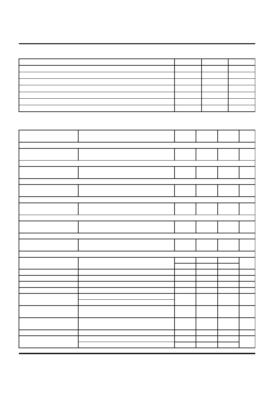
ABSOULTE MAXIMUM RATINS
CHARACTERISTIC
Supply Voltage
Operating Junction Temperature Range
Storage Temperature Range
Thermal Resistance Junction to Case TO-263
Thermal Resistance Junction to Ambient TO-263
Lead Temperature (Soldering) 10 sec.
Maximum Output Current
ELECTRICAL CHARACTERISTICS I
OUT
=100, T
A
=25, unless otherwise specified
Min. Load Current(Note 3)
Line Regulation (V
REF
(V
IN
))
Load Regulation (V
REF
(V
OUT
))
Dropout Voltage
Current Limit
I
OUT
(MAX)
Thermal Regulation
(V
OUT
(Pwr))
Output Noise, RMS
HTC
SYMBOL
Tstg
-65~150
UNIT
V
VALUE
C/W
C/W
A
A
0.3
1
1.7
2.5
0.02
60
MIN
TYP
MAX
1.485
1.5
1.515
2.475
3
Thermal Resistance
Junction to Tab
Junction to Ambient
T
A
=125, 1000Hrs
10Hz to 10Khz T
A
=25
0.05
0.01
Long Term Stability
T
A
=25, 30 pulse
Vin-Vout=3V
1.4V(V
IN
-V
OUT
) Adjustable Only
1.25
1.27
1.225
1.25
1.27
1.225
0.003
3.3V Version
1.5V Version
0<I
OUT
<1.5A, 4.75V<V
IN
<7V
2.5
2.525
3.27
3.3
3.33
V
2.879
Tjc
3
Vin
7
Topr
0~125
Tja
60
Tsol
300
Imax
1.5
3.0V Version
Output Voltage
0<I
OUT
<1.5A, 4.5V<V
IN
<7V
2.97
3
3.03
2.5V Version
V
%/Vo
/W
%/W
%
%
V
0.3
1.2
V
mA
%
5
10
0.005
1.5V(V
IN-
V
OUT
)5.75V, 10I
OUT
1.5A
4.95
5
1.1
1.5V(V
IN-
V
OUT
)5.75V
2.75VV
IN
7V, I
OUT
=10, T
J
=25
10I
OUT
1.5A,(V
IN
-V
OUT
)=3V,T
J
=25
V
REF
=1% , Iout=1.5A
V
V
5.0V Version
0.2
Reference Voltage (V
REF
)
V
Output Voltage
All Voltage Options
0I
OUT
1.5A, 5.5VV
IN
<7V
V
IN
7V,PP
MAX
0<I
OUT
<1.5A, 3.5V<V
IN
<7V
2.85V Version
Output Voltage
0<I
OUT
<1.5A, 4.35V<V
IN
<7V
2.822
2.85
2
V
UNIT
0<I
OUT
<1.5A, 2.75V<V
IN
<7V
PARAMETER
Output Voltage
TEST CONDITIONS
Output Voltage
Output Voltage
5.05