MSP 34x5G
Multistandard
Sound Processor Family
Edition March 5, 2001
6251-480-3PD
PRELIMINARY DATA SHEET
MICRONAS
MICRONAS

MSP 34x5G
PRELIMINARY DATA SHEET
2
Micronas
Contents
Page
Section
Title
5
1.
Introduction
6
1.1.
Features of the MSP 34x5G Family and Differences to MSPD
6
1.2.
MSP 34x5G Version List
7
1.3.
MSP 34x5G Versions and their Application Fields
8
2.
Functional Description
9
2.1.
Architecture of the MSP 34x5G Family
9
2.2.
Sound IF Processing
9
2.2.1.
Analog Sound IF Input
9
2.2.2.
Demodulator: Standards and Features
10
2.2.3.
Preprocessing of Demodulator Signals
10
2.2.4.
Automatic Sound Select
10
2.2.5.
Manual Mode
12
2.3.
Preprocessing for SCART and I
2
S Input Signals
12
2.4.
Source Selection and Output Channel Matrix
12
2.5.
Audio Baseband Processing
12
2.5.1.
Automatic Volume Correction (AVC)
12
2.5.2.
Loudspeaker Outputs
12
2.5.3.
Quasi-Peak Detector
13
2.6.
SCART Signal Routing
13
2.6.1.
SCART DSP In and SCART Out Select
13
2.6.2.
Stand-by Mode
13
2.7.
I
2
S Bus Interface
14
2.8.
ADR Bus Interface
14
2.9.
Digital Control I/O Pins and Status Change Indication
14
2.10.
Clock PLL Oscillator and Crystal Specifications
15
3.
Control Interface
15
3.1.
I
2
C Bus Interface
15
3.1.1.
Internal Hardware Error Handling
16
3.1.2.
Description of CONTROL Register
16
3.1.3.
Protocol Description
17
3.1.4.
Proposals for General MSP 34x5G I
2
C Telegrams
17
3.1.4.1.
Symbols
17
3.1.4.2.
Write Telegrams
17
3.1.4.3.
Read Telegrams
17
3.1.4.4.
Examples
17
3.2.
Start-Up Sequence: Power-Up and I
2
C-Controlling
17
3.3.
MSP 34x5G Programming Interface
17
3.3.1.
User Registers Overview
20
3.3.2.
Description of User Registers
21
3.3.2.1.
STANDARD SELECT Register
21
3.3.2.2.
Refresh of STANDARD SELECT Register
21
3.3.2.3.
STANDARD RESULT Register
23
3.3.2.4.
Write Registers on I
2
C Subaddress 10
hex
25
3.3.2.5.
Read Registers on I
2
C Subaddress 11
hex
26
3.3.2.6.
Write Registers on I
2
C Subaddress 12
hex

Contents, continued
Page
Section
Title
PRELIMINARY DATA SHEET
MSP 34x5G
Micronas
3
36
3.3.2.7.
Read Registers on I
2
C Subaddress 13
hex
37
3.4.
Programming Tips
37
3.5.
Examples of Minimum Initialization Codes
37
3.5.1.
B/G-FM (A2 or NICAM)
37
3.5.2.
BTSC-Stereo
37
3.5.3.
BTSC-SAP with SAP at Loudspeaker Channel
38
3.5.4.
FM-Stereo Radio
38
3.5.5.
Automatic Standard Detection
38
3.5.6.
Software Flow for Interrupt driven STATUS Check
40
4.
Specifications
40
4.1.
Outline Dimensions
42
4.2.
Pin Connections and Short Descriptions
45
4.3.
Pin Description
47
4.4.
Pin Configurations
51
4.5.
Pin Circuits
53
4.6.
Electrical Characteristics
53
4.6.1.
Absolute Maximum Ratings
54
4.6.2.
Recommended Operating Conditions
54
4.6.2.1.
General Recommended Operating Conditions
54
4.6.2.2.
Analog Input and Output Recommendations
55
4.6.2.3.
Recommendations for Analog Sound IF Input Signal
56
4.6.2.4.
Crystal Recommendations
58
4.6.3.
Characteristics
58
4.6.3.1.
General Characteristics
59
4.6.3.2.
Digital Inputs, Digital Outputs
60
4.6.3.3.
Reset Input and Power-Up
61
4.6.3.4.
I
2
C Bus Characteristics
62
4.6.3.5.
I
2
S-Bus Characteristics
64
4.6.3.6.
Analog Baseband Inputs and Outputs, AGNDC
65
4.6.3.7.
Sound IF Input
65
4.6.3.8.
Power Supply Rejection
66
4.6.3.9.
Analog Performance
69
4.6.3.10.
Sound Standard Dependent Characteristics
73
5.
Appendix A: Overview of TV Sound Standards
73
5.1.
NICAM 728
74
5.2.
A2 Systems
75
5.3.
BTSC-Sound System
75
5.4.
Japanese FM Stereo System (EIA-J)
76
5.5.
FM Satellite Sound
76
5.6.
FM-Stereo Radio
77
6.
Appendix B: Manual/Compatibility Mode
77
6.1.
Demodulator Write and Read Registers for Manual/Compatibility Mode
78
6.2.
DSP Write and Read Registers for Manual/Compatibility Mode
79
6.3.
Manual/Compatibility Mode: Description of Demodulator Write Registers
79
6.3.1.
Automatic Switching between NICAM and Analog Sound

MSP 34x5G
PRELIMINARY DATA SHEET
4
Micronas
Contents, continued
Page
Section
Title
79
6.3.1.1.
Function in Automatic Sound Select Mode
79
6.3.1.2.
Function in Manual Mode
81
6.3.2.
A2 Threshold
81
6.3.3.
Carrier-Mute Threshold
82
6.3.4.
Register AD_CV
83
6.3.5.
Register MODE_REG
85
6.3.6.
FIR-Parameter, Registers FIR1 and FIR2
85
6.3.7.
DCO-Registers
87
6.4.
Manual/Compatibility Mode: Description of Demodulator Read Registers
87
6.4.1.
NICAM Mode Control/Additional Data Bits Register
87
6.4.2.
Additional Data Bits Register
87
6.4.3.
CIB Bits Register
88
6.4.4.
NICAM Error Rate Register
88
6.4.5.
PLL_CAPS Readback Register
88
6.4.6.
AGC_GAIN Readback Register
88
6.4.7.
Automatic Search Function for FM-Carrier Detection in Satellite Mode
89
6.5.
Manual/Compatibility Mode: Description of DSP Write Registers
89
6.5.1.
Additional Channel Matrix Modes
89
6.5.2.
Volume Modes of SCART1 Output
89
6.5.3.
FM Fixed Deemphasis
89
6.5.4.
FM Adaptive Deemphasis
89
6.5.5.
NICAM Deemphasis
90
6.5.6.
Identification Mode for A2 Stereo Systems
90
6.5.7.
FM DC Notch
90
6.6.
Manual/Compatibility Mode: Description of DSP Read Registers
90
6.6.1.
Stereo Detection Register for A2 Stereo Systems
90
6.6.2.
DC Level Register
91
6.7.
Demodulator Source Channels in Manual Mode
91
6.7.1.
Terrestric Sound Standards
91
6.7.2.
SAT Sound Standards
91
6.8.
Exclusions of Audio Baseband Features
91
6.9.
Compatibility Restrictions to MSP 34x5D
93
7.
Appendix D: Application Information
93
7.1.
Phase Relationship of Analog Outputs
94
7.2.
Application Circuit
96
8.
Appendix E: MSP 34x5G Version History
96
9.
Data Sheet History
License Notice:
"Dolby Pro Logic" is a trademark of Dolby Laboratories.
Supply of this implementation of Dolby Technology does not convey a license nor imply a right under any patent, or any other industrial or intellec-
tual property right of Dolby Laboratories, to use this implementation in any finished end-user or ready-to-use final product. Companies planning to
use this implementation in products must obtain a license from Dolby Laboratories Licensing Corporation before designing such products.

PRELIMINARY DATA SHEET
MSP 34x5G
Micronas
5
Multistandard Sound Processor Family
Release Note: Revision bars indicate significant
changes to the previous edition. The hardware and
software description in this document is valid for
the MSP 34x5G version B8 and following versions.
1. Introduction
The MSP 34x5G family of single-chip Multistandard
Sound Processors covers the sound processing of all
analog TV standards worldwide, as well as the NICAM
digital sound standards. The full TV sound processing,
starting with analog sound IF signal-in, down to pro-
cessed analog AF-out, is performed in a single chip.
Figure 1�1 shows a simplified functional block diagram
of the MSP 34x5G.
These TV sound processing ICs include versions for
processing the multichannel television sound (MTS)
signal conforming to the standard recommended by
the Broadcast Television Systems Committee (BTSC).
The DBX noise reduction, or alternatively, Micronas
Noise Reduction (MNR) is performed alignment free.
Other processed standards are the Japanese FM-FM
multiplex standard (EIA-J) and the FM-Stereo-Radio
standard.
Current ICs have to perform adjustment procedures in
order to achieve good stereo separation for BTSC and
EIA-J. The MSP 34x5G has optimum stereo perfor-
mance without any adjustments.
All MSP 34xxG versions are pin compatible to the
MSP 34xxD. Only minor modifications are necessary
to adapt a MSP 34xxD controlling software to the
MSP 34xxG. The MSP 34x5G further simplifies con-
trolling software. Standard selection requires a single
I
2
C transmission only.
Note: The MSP 34x5G version has reduced control
registers and less functional pins. The remaining regis-
ters are software-compatible to the MSP 34x0G. The
pinning is compatible to the MSP 34x0G.
The MSP 34x5G has built-in automatic functions: The
IC is able to detect the actual sound standard automat-
ically (Automatic Standard Detection). Furthermore,
pilot levels and identification signals can be evaluated
internally with subsequent switching between mono/
stereo/bilingual; no I
2
C interaction is necessary (Auto-
matic Sound Selection).
The MSP 34x5G can handle very high FM deviations
even in conjunction with NICAM processing. This is
especially important for the introduction of NICAM in
China.
The ICs are produced in submicron CMOS technology.
The MSP 34x5G is available in the following packages:
PSDIP64, PSDIP52, PMQFP44, PLQFP64, and
PQFP80.
Fig. 1�1: Simplified functional block diagram of MSP 34x5G
Sour
ce Sel
e
ct
Loud-
SCART1
SCART1
SCART2
MONO
De-
modulator
speaker
Sound
Processing
DAC
ADC
Loud-
DAC
ADC
Sound IF1
speaker
I
2
S
I
2
S1
I
2
S2
Pre-
processing
Prescale
Prescale
SCART
DSP
Input
Select
SCART
Output
Select

MSP 34x5G
PRELIMINARY DATA SHEET
6
Micronas
1.1. Features of the MSP 34x5G Family and Differences to MSPD
1.2. MSP 34x5G Version List
Feature
(New features not available for MSPD are shaded gray.)
3405
3415
3425
3445
3455
3465
Standard Selection with single I
2
C transmission
X
X
X
X
X
X
Automatic Standard Detection of terrestrial TV standards
X
X
X
X
X
X
Automatic Sound Selection (mono/stereo/bilingual), new registers MODUS, STATUS
X
X
X
X
X
X
Automatic Carrier Mute function
X
X
X
X
X
X
Interrupt output programmable (indicating status change)
X
X
X
X
X
X
Loudspeaker channel with volume, balance, bass, treble, loudness
X
X
X
X
X
X
AVC: Automatic Volume Correction
X
X
X
X
X
X
Spatial effect for loudspeaker channel
X
X
X
X
X
X
Two Stereo SCART (line) inputs, one Mono input; one Stereo SCART outputs
X
X
X
X
X
X
Complete SCART in/out switching matrix
X
X
X
X
X
X
Two I
2
S inputs; one I
2
S output
X
X
X
X
X
X
All analog Mono sound carriers including AM-SECAM L
X
X
X
X
X
X
All analog FM-Stereo A2 and satellite standards
X
X
X
All NICAM standards
X
X
Simultaneous demodulation of (very) high-deviation FM-Mono and NICAM
X
X
Adaptive deemphasis for satellite (Wegener-Panda, acc. to ASTRA specification)
X
X
X
X
ASTRA Digital Radio (ADR) together with DRP 3510A
X
X
X
Demodulation of the BTSC multiplex signal and the SAP channel
X
X
X
Alignment free digital DBX noise reduction for BTSC Stereo and SAP
X
X
Alignment free digital Micronas Noise Reduction (MNR) for BTSC Stereo and SAP
X
BTSC stereo separation (MSP 3425/45G also EIA-J) significantly better than spec.
X
X
X
SAP and stereo detection for BTSC system
X
X
X
Korean FM-Stereo A2 standard
X
X
X
X
X
Alignment-free Japanese standard EIA-J
X
X
X
Demodulation of the FM-Radio multiplex signal
X
X
X
Version
Status
Description
MSP 3405G
available
FM Stereo (A2) Version
MSP 3415G
available
NICAM and FM Stereo (A2) Version
MSP 3425G
available
NTSC Version (A2 Korea, BTSC with Micronas Noise Reduction (MNR), Japanese EIA-J system)
MSP 3445G
available
NTSC Version (A2 Korea, BTSC with DBX noise reduction, Japanese EIA-J system)
MSP 3455G
available
Global Stereo Version (all sound standards)
MSP 3465G
available
Global Mono Version (all sound standards)

PRELIMINARY DATA SHEET
MSP 34x5G
Micronas
7
1.3. MSP 34x5G Versions and their Application Fields
Table 1�1 provides an overview of TV sound standards
that can be processed by the MSP 34x5G family. In
addition, the MSP 34x5G is able to handle the FM-
Radio standard. With the MSP 34x5G, a complete
multimedia receiver covering all TV sound standards
together with terrestrial/cable and satellite radio sound
can be built; even ASTRA Digital Radio can be pro-
cessed (with a DRP 3510A coprocessor).
Fig. 1�2: Typical MSP 34x5G application
Table 1�1: TV Stereo Sound Standards covered by the MSP 34x5G IC Family (details see Appendix A)
MSP Version
TV-
System
Position of Sound
Carrier /MHz
Sound
Modulation
Color
System
Broadcast e.g. in:
3405
3415
3455
B/G
5.5/5.7421875
FM-Stereo (A2)
PAL
Germany
5.5/5.85
FM-Mono/NICAM
PAL
Scandinavia, Spain
L
6.5/5.85
AM-Mono/NICAM
SECAM-L
France
I
6.0/6.552
FM-Mono/NICAM
PAL
UK, Hong Kong
3405
D/K
6.5/6.2578125
FM-Stereo (A2, D/K1)
SECAM-East
Slovak. Rep.
6.5/6.7421875
FM-Stereo (A2, D/K2)
PAL
currently no broadcast
6.5/5.7421875
FM-Stereo (A2, D/K3)
SECAM-East
Poland
6.5/5.85
FM-Mono/NICAM (D/K, NICAM)
PAL
China, Hungary
3405
Satellite
6.5
7.02/7.2
7.38/7.56
etc.
FM-Mono
FM-Stereo
ASTRA Digital Radio (ADR)
with DRP 3510A
PAL
Europe Sat.
ASTRA
3425,
3445
M/N
4.5/4.724212
FM-Stereo (A2)
NTSC
Korea
4.5
FM-FM (EIA-J)
NTSC
Japan
4.5
BTSC-Stereo
+
SAP
NTSC, PAL
USA, Argentina
FM-Radio
10.7
FM-Stereo Radio
USA, Europe
3465
All standards as above, but Mono demodulation only.
33
34 39 MHz
4.5 9 MHz
2
MSP 34x5G
2
2
1
Tuner
SAW Filter
Vision
Demo-
dulator
Composite
Video
Sound
IF
Mixer
SCART
Inputs
Mono
SCART1
SCART2
Loudspeaker
SCART Output
SCART1
Dolby
Pro Logic
Processor
DPL 351xA
ADR
Decoder
DRP 3510A
I
2
S1
ADR
I
2
S2
MSP 34x5G
PR
EL
I
M
IN
A
R
Y D
A
TA
SH
EE
T
8
M
i
c
r
onas
2
.
F
unc
t
i
ona
l De
s
c
r
i
ption
I
2
C
Stereo or B
Stereo or A
FM/AM
FM/AM
Prescale
Prescale
NICAM
Read
Register
Deemphasis:
50/75
�
s,
J17
DBX/MNR
Standard
DEMODULATOR
(incl. Carrier Mute)
Decoded
-
NICAM
-
A2
-
AM
-
BTSC
-
EIA-J
-
SAT
-
FM-Radio
and Sound
Detection
Standards:
Deemphasis
J17
Stereo or A/B
Automatic
Sound Select
S t a n d a r d S e l e c t i o n
(0E
hex
)
(10
hex
)
I
2
C
Read
Register
D
A
SCART1
Channel
Matrix
Volume
S
o
u
r
ce S
e
lect
Quasi-Peak
Detector
Quasi-Peak
Channel
Matrix
Loud-
speaker
Channel
Matrix
A
D
A
D
SCA
R
T
DSP I
n
p
u
t
S
e
le
c
t
S
C
A
R
T Ou
tput S
e
l
e
ct
SCART1_L/R
0
1
3
4
5
2
6
(0D
hex
)
(08
hex
)
(0C
hex
)
(0A
hex
)
(07
hex
)
(00
hex
)
(29
hex
)
(14
hex
)
Fig. 2�1: Signal flow block diagram of the MSP 34x5G (input and output names correspond to pin names).
(13
hex
)
(13
hex
)
Bass/
Treble
Volume
Loud-
ness
Spatial
Effects
AVC
Balance
D
A
Beeper
(02
hex
)
(03
hex
)
(04
hex
)
(05
hex
)
(01
hex
)
DACM_L
DACM_R
I
2
S
Channel
Matrix
I
2
S
Interface
(0B
hex
)
I
2
S
Interface
I
2
S
Interface
I
2
S1
I
2
S2
Prescale
Prescale
SCART
Prescale
SC1_IN_L
SC1_IN_R
SC2_IN_L
SC2_IN_R
MONO_IN
ANA_IN1+
ADR-Bus
Interface
AGC
I2S_DA_IN1
I2S_DA_IN2
(16
hex
)
(12
hex
)
I2S_DA_OUT
SC1_OUT_L
SC1_OUT_R
(19
hex
)
(1A
hex
)
Panda1

PRELIMINARY DATA SHEET
MSP 34x5G
Micronas
9
2.1. Architecture of the MSP 34x5G Family
Fig. 2�1 on page 8 shows a simplified block diagram of
the IC. The block diagram contains all features of the
MSP 3455G. Other members of the MSP 34x5G family
do not have the complete set of features: The demodu-
lator handles only a subset of the standards presented
in the demodulator block; NICAM processing is only
possible in the MSP 3415G and MSP 3455G (see
dashed block in Fig. 2�1).
2.2. Sound IF Processing
2.2.1. Analog Sound IF Input
The input pins ANA_IN1+ and ANA_IN
-
offer the pos-
sibility to connect sound IF (SIF) sources to the
MSP 34x5G. The analog-to-digital conversion of the
sound IF signal is done by an A/D-converter. An ana-
log automatic gain circuit (AGC) allows a wide range of
input levels. The high-pass filter formed by the cou-
pling capacitor at pin ANA_IN1+ (see Section 7.
"Appendix D: Application Information" on page 93) is
sufficient in most cases to suppress video compo-
nents. Some combinations of SAW filters and sound IF
mixer ICs, however, show large picture components on
their outputs. In this case, further filtering is recom-
mended.
2.2.2. Demodulator: Standards and Features
The MSP 34x5G is able to demodulate all TV sound
standards worldwide including the digital NICAM sys-
tem. Depending on the MSP 34x5G version, the fol-
lowing demodulation modes can be performed:
A2-Systems: Detection and demodulation of two sep-
arate FM carriers (FM1 and FM2), demodulation and
evaluation of the identification signal of carrier FM2.
NICAM-Systems: Demodulation and decoding of the
NICAM carrier, detection and demodulation of the ana-
log (FM or AM) carrier. For D/K-NICAM, the FM carrier
may have a maximum deviation of 384 kHz.
Very high deviation FM-Mono: Detection and robust
demodulation of one FM carrier with a maximum devi-
ation of 540 kHz.
BTSC-Stereo: Detection and FM demodulation of the
aural carrier resulting in the MTS/MPX signal. Detec-
tion and evaluation of the pilot carrier, AM demodula-
tion of the (L-R)-carrier and detection of the SAP sub-
carrier. Processing of the DBX noise reduction or
Micronas Noise Reduction (MNR).
BTSC-Mono + SAP: Detection and FM demodulation
of the aural carrier resulting in the MTS/MPX signal.
Detection and evaluation of the pilot carrier, detection
and FM demodulation of the SAP-subcarrier. Process-
ing of the DBX noise reduction or Micronas Noise
Reduction (MNR).
Japan Stereo: Detection and FM demodulation of the
aural carrier resulting in the MPX signal. Demodulation
and evaluation of the identification signal and FM
demodulation of the (L-R)-carrier.
FM-Satellite Sound: Demodulation of one or two FM
carriers. Processing of high-deviation mono or narrow
bandwidth mono, stereo, or bilingual satellite sound
according to the ASTRA specification.
FM-Stereo-Radio: Detection and FM demodulation of
the aural carrier resulting in the MPX signal. Detection
and evaluation of the pilot carrier and AM demodula-
tion of the (L-R)-carrier.
The demodulator blocks of all MSP 34x5G versions
have identical user interfaces. Even completely differ-
ent systems like the BTSC and NICAM systems are
controlled the same way. Standards are selected by
means of MSP Standard Codes. Automatic processes
handle standard detection and identification without
controller interaction. The key features of the
MSP 34x5G demodulator blocks are
Standard Selection: The controlling of the demodula-
tor is minimized: All parameters, such as tuning fre-
quencies or filter bandwidth, are adjusted automati-
cally by transmitting one single value to the
STANDARD SELECT register. For all standards, spe-
cific MSP standard codes are defined.
Automatic Standard Detection: If the TV sound stan-
dard is unknown, the MSP 34x5G can automatically
detect the actual standard, switch to that standard, and
respond the actual MSP standard code.
Automatic Carrier Mute: To prevent noise effects or
FM identification problems in the absence of an FM
carrier, the MSP 34x5G offers a configurable carrier
mute feature, which is activated automatically if the TV
sound standard is selected by means of the STAN-
DARD SELECT register. If no FM carrier is detected at
one of the two MSP demodulator channels, the corre-
sponding demodulator output is muted. This is indi-
cated in the STATUS register.

MSP 34x5G
PRELIMINARY DATA SHEET
10
Micronas
2.2.3. Preprocessing of Demodulator Signals
The NICAM signals must be processed by a deempha-
sis filter and adjusted in level. The analog demodu-
lated signals must be processed by a deemphasis fil-
ter, adjusted in level, and dematrixed. The correct
deemphasis filters are already selected by setting the
standard in the STANDARD SELECT register. The
level adjustment has to be done by means of the FM/
AM and NICAM prescale registers. The necessary
dematrix function depends on the selected sound
standard and the actual broadcasted sound mode
(mono, stereo, or bilingual). It can be manually set by
the FM Matrix Mode register or automatically by the
Automatic Sound Selection.
2.2.4. Automatic Sound Select
In the Automatic Sound Select mode, the dematrix
function is automatically selected based on the identifi-
cation information in the STATUS register. No I
2
C inter-
action is necessary when the broadcasted sound
mode changes (e.g. from mono to stereo).
The demodulator supports the identification check by
switching between mono-compatible standards (stan-
dards that have the same FM-Mono carrier) automati-
cally and non-audible. If B/G-FM or B/G-NICAM is
selected, the MSP will switch between these stan-
dards. The same action is performed for the standards:
D/K1-FM, D/K2-FM, D/K3-FM and D/K-NICAM.
Switching is only done in the absence of any stereo or
bilingual identification. If identification is found, the
MSP keeps the detected standard.
In case of high bit-error rates, the MSP 34x5G auto-
matically falls back from digital NICAM sound to ana-
log FM or AM mono.
Table 2�1 summarizes all actions that take place when
Automatic Sound Select is switched on.
To provide more flexibility, the Automatic Sound Select
block prepares four different source channels of
demodulated sound (Fig. 2�2). By choosing one of the
four demodulator channels, the preferred sound mode
can be selected for each of the output channels (loud-
speaker, headphone, etc.). This is done by means of
the Source Select registers.
The following source channels of demodulated sound
are defined:
� "FM/AM" channel: Analog mono sound, stereo if
available. In case of NICAM, analog mono only
(FM or AM mono).
� "Stereo or A/B" channel: Analog or digital mono
sound, stereo if available. In case of bilingual broad-
cast, it contains both languages A (left) and B
(right).
� "Stereo or A" channel: Analog or digital mono
sound, stereo if available. In case of bilingual broad-
cast, it contains language A (on left and right).
� "Stereo or B" channel: Analog or digital mono
sound, stereo if available. In case of bilingual broad-
cast, it contains language B (on left and right).
Fig. 2�2 and Table 2�2 show the source channel
assignment of the demodulated signals in case of
Automatic Sound Select mode for all sound standards.
Note: The analog primary input channel contains the
signal of the mono FM/AM carrier or the L+R signal of
the MPX carrier. The secondary input channel con-
tains the signal of the 2nd FM carrier, the L-R signal of
the MPX carrier, or the SAP signal.
Fig. 2�2: Source channel assignment of demodulated
signals in Automatic Sound Select Mode
2.2.5. Manual Mode
Fig. 2�3 shows the source channel assignment of
demodulated signals in case of manual mode. If man-
ual mode is required, more information can be found in
Section 6.7. "Demodulator Source Channels in Manual
Mode" on page 91.
Fig. 2�3: Source channel assignment of demodulated
signals in Manual Mode
S
o
u
r
ce S
e
lect
FM/AM
Stereo or A/B
Stereo or A
Stereo or B
0
1
3
4
primary
FM/AM
Prescale
NICAM
Prescale
Automatic
Sound
Select
channel
secondary
channel
NICAM A
NICAM B
LS Ch.
Matrix
Output-Ch.
matrices
must be set
once to
stereo.
S
o
ur
ce S
e
lect
FM/AM
(Stereo or A/B)
0
1
primary
FM/AM
Prescale
NICAM
Prescale
FM-Matrix
channel
secondary
channel
NICAM A
NICAM B
LS Ch.
Matrix
Output-Ch.
matrices
must be set
according to
the standard.
NICAM
PRELIMINARY DATA SHEET
MSP 34x5G
Micronas
11
Table 2�1: Performed actions of the Automatic Sound Selection
Selected TV Sound Standard
Performed Actions
B/G-FM, D/K-FM, M-Korea,
and M-Japan
Evaluation of the identification signal and automatic switching to mono, stereo, or bilingual. Preparing four
demodulator source channels according to Table 2�2.
B/G-NICAM, L-NICAM, I-NICAM,
D/K-NICAM
Evaluation of NICAM-C-bits and automatic switching to mono, stereo, or bilingual. Preparing four
demodulator source channels according to Table 2�2.
In case of bad or no NICAM reception, the MSP switches automatically to FM/AM mono and switches
back to NICAM if possible. A hysteresis prevents periodical switching.
B/G-FM, B/G-NICAM
or
D/K1-FM, D/K2-FM, D/K3-FM,
and D/K-NICAM
Automatic searching for stereo/bilingual-identification in case of mono transmission. Automatic and non-
audible changes between Dual-FM and FM-NICAM standards while listening to the basic FM-mono sound
carrier.
Example: If starting with B/G-FM-Stereo, there will be a periodical alternation to B/G-NICAM in the
absence of FM-Stereo/Bilingual or NICAM-identification. Once an identification is detected, the MSP
keeps the corresponding standard.
BTSC-STEREO, FM Radio
Evaluation of the pilot signal and automatic switching to mono or stereo. Preparing four demodulator
source channels according to Table 2�2. Detection of the SAP carrier.
M-BTSC-SAP
In the absence of SAP, the MSP switches to BTSC-stereo if available. If SAP is detected, the MSP
switches automatically to SAP (see Table 2�2).
Table 2�2: Sound modes for the demodulator source channels with Automatic Sound Select
Source Channels in Automatic Sound Select Mode
Broadcasted
Sound
Standard
Selected
MSP Standard
Code
3)
Broadcasted
Sound Mode
FM/AM
(source select: 0)
Stereo or A/B
(source select: 1)
Stereo or A
(source select: 3)
Stereo or B
(source select: 4)
M-Korea
B/G-FM
D/K-FM
M-Japan
02
03, 08
1)
04, 05, 07, 0B
1)
30
MONO Mono
Mono
Mono
Mono
STEREO
Stereo
Stereo
Stereo
Stereo
BILINGUAL:
Languages A and B
Right = B
Left = A
Right = B
A
B
B/G-NICAM
L-NICAM
I-NICAM
D/K-NICAM
D/K-NICAM
(with high
deviation FM)
08, 03
2)
09
0A
0B, 04
2)
, 05
2)
0C, 0D
NICAM not available or
error rate too high
analog Mono
analog Mono
analog Mono
analog Mono
MONO
analog Mono
NICAM Mono
NICAM Mono
NICAM Mono
STEREO
analog Mono
NICAM Stereo
NICAM Stereo
NICAM Stereo
BILINGUAL:
Languages A and B
analog Mono
Left = NICAM A
Right = NICAM B
NICAM A
NICAM B
BTSC
20, 21
MONO
Mono
Mono
Mono
Mono
STEREO
Stereo
Stereo
Stereo
Stereo
20
MONO + SAP
Mono
Mono
Mono
Mono
STEREO + SAP
Stereo
Stereo
Stereo
Stereo
21
MONO + SAP
Left = Mono
Right = SAP
Left = Mono
Right = SAP
Mono
SAP
STEREO + SAP
Left = Mono
Right = SAP
Left = Mono
Right = SAP
Mono
SAP
FM Radio
40
MONO
Mono
Mono
Mono
Mono
STEREO
Stereo
Stereo
Stereo
Stereo
1)
The Automatic Sound Select process will automatically switch to the mono compatible analog standard.
2)
The Automatic Sound Select process will automatically switch to the mono compatible digital standard.
3)
The MSP Standard Codes are defined in Table 3�7 on page 20.

MSP 34x5G
PRELIMINARY DATA SHEET
12
Micronas
2.3. Preprocessing for SCART and
I
2
S Input Signals
The SCART and I
2
S inputs need only be adjusted in
level by means of the SCART and I
2
S prescale regis-
ters.
2.4. Source Selection and Output Channel Matrix
The Source Selector makes it possible to distribute all
source signals (one of the demodulator source chan-
nels or SCART) to the desired output channels (loud-
speaker, etc.). All input and output signals can be pro-
cessed simultaneously. Each source channel is
identified by a unique source address.
For each output channel, the sound mode can be set
to sound A, sound B, stereo, or mono by means of the
output channel matrix.
If Automatic Sound Select is on, the output channel
matrix can stay fixed to stereo (transparent) for demod-
ulated signals.
2.5. Audio Baseband Processing
2.5.1. Automatic Volume Correction (AVC)
Different sound sources (e.g. terrestrial channels, SAT
channels, or SCART) fairly often do not have the same
volume level. Advertisements during movies usually
have a higher volume level than the movie itself. This
results in annoying volume changes. The AVC solves
this problem by equalizing the volume level.
To prevent clipping, the AVC's gain decreases quickly
in dynamic boost conditions. To suppress oscillation
effects, the gain increases rather slowly for low level
inputs. The decay time is programmable by means of
the AVC register (see page 30).
For input signals ranging from
-
24 dBr to 0 dBr, the
AVC maintains a fixed output level of
-
18 dBr. Fig. 2�4
shows the AVC output level versus its input level. For
prescale and volume registers set to 0 dB, a level of
0 dBr corresponds to full scale input/output. This is
� SCART input/output 0 dBr = 2.0 V
rms
� Loudspeaker output 0 dBr = 1.4 V
rms
Fig. 2�4: Simplified AVC characteristics
2.5.2. Loudspeaker Outputs
The following baseband features are implemented in
the loudspeaker output channels: bass/treble, loud-
ness, balance, and volume. A square wave beeper can
be added to the loudspeaker channel.
2.5.3. Quasi-Peak Detector
The quasi-peak readout register can be used to read
out the quasi-peak level of any input source. The fea-
ture is based on following filter time constants:
attack time: 1.3 ms
decay time: 37 ms
-
30
-
24
-
18
-
12
-
6
input level
-
18
-
24
output level
0
[dBr]
[dBr]

PRELIMINARY DATA SHEET
MSP 34x5G
Micronas
13
2.6. SCART Signal Routing
2.6.1. SCART DSP In and SCART Out Select
The SCART DSP Input Select and SCART Output
Select blocks include full matrix switching facilities. To
design a TV set with two pairs of SCART-inputs and
one pair of SCART-outputs, no external switching
hardware is required. The switches are controlled by
the ACB user register (see page 34).
2.6.2. Stand-by Mode
If the MSP 34x5G is switched off by first pulling
STANDBYQ low and then (after >1
�
s delay) switching
off DVSUP and AVSUP, but keeping AHVSUP
(`Stand-by'-mode), the SCART switches maintain
their position and function. This allows the copying
from selected SCART-inputs to SCART-outputs in the
TV set's stand-by mode.
In case of power on or starting from stand-by (switch-
ing on the DVSUP and AVSUP, RESETQ going high
2 ms later), all internal registers except the ACB regis-
ter (page 34) are reset to the default configuration (see
Table 3�5 on page 18). The reset position of the ACB
register becomes active after the first I
2
C transmission
into the Baseband Processing part. By transmitting the
ACB register first, the reset state can be redefined.
2.7. I
2
S Bus Interface
The MSP 34x5G has a synchronous master/slave
input/output interface running on 32 kHz.
The interface accepts two formats:
1. I
2
S_WS changes at the word boundary
2. I
2
S_WS changes one I
2
S-clock period before the
word boundaries.
All I
2
S options are set by means of the MODUS and
the I2S_CONFIG registers.
The I
2
S bus interface consists of five pins:
� I2S_DA_IN1, I2S_DA_IN2:
I
2
S serial data input: 16, 18....32 bits per sample
� I2S_DA_OUT:
I
2
S serial data output: 16, 18...32 bits per sample
� I2S_CL:
I
2
S serial clock
� I2S_WS:
I
2
S word strobe signal defines the left and right
sample
If the MSP 34x5G serves as the master on the I
2
S
interface, the clock and word strobe lines are driven by
the IC. In this mode, only 16 or 32 bits per sample can
be selected. In slave mode, these lines are input to the
IC and the MSP clock is synchronized to 576 times the
I2S_WS rate (32 kHz). NICAM operation is not possi-
ble in slave mode.
An I
2
S timing diagram is shown in Fig. 4�28 on
page 63.

MSP 34x5G
PRELIMINARY DATA SHEET
14
Micronas
2.8. ADR Bus Interface
For the ASTRA Digital Radio System (ADR), the
MSP 3405G, MSP 3415G, and MSP 3455G performs
preprocessing such as carrier selection and filtering.
Via the 3-line ADR-bus, the resulting signals are trans-
ferred to the DRP 3510A coprocessor, where the
source decoding is performed. To be prepared for an
upgrade to ADR with an additional DRP board, the fol-
lowing lines of MSP 34x5G should be provided on a
feature connector:
� I2S_DA_IN1 or I2S_DA_IN2
� I2S_DA_OUT
� I2S_WS
� I2S_CL
� ADR_CL, ADR_WS, ADR_DA
For more details, please refer to the DRP 3510A data
sheet.
2.9. Digital Control I/O Pins and
Status Change Indication
The static level of the digital input/output pins
D_CTR_I/O_0/1 is switchable between HIGH and
LOW via the I
2
C-bus by means of the ACB register
(see page 34). This enables the controlling of external
hardware switches or other devices via I
2
C-bus.
The digital input/output pins can be set to high imped-
ance by means of the MODUS register (see page 23).
In this mode, the pins can be used as input. The cur-
rent state can be read out of the STATUS register (see
page 25).
Optionally, the pin D_CTR_I/O_1 can be used as an
interrupt request signal to the controller, indicating any
changes in the read register STATUS. This makes poll-
ing unnecessary; I
2
C-bus interactions are reduced to a
minimum (see STATUS register on page 25 and
MODUS register on page 23).
2.10. Clock PLL Oscillator and
Crystal Specifications
The MSP 34x5G derives all internal system clocks
from the 18.432 MHz oscillator. In NICAM or in I
2
S-
Slave mode, the clock is phase-locked to the corre-
sponding source. Therefore, it is not possible to use
NICAM and I
2
S-Slave mode at the same time.
For proper performance, the MSP clock oscillator
requires a 18.432-MHz crystal. Note, that for the
phase-locked mode (NICAM, I
2
S slave), crystals with
tighter tolerance are required.
PRELIMINARY DATA SHEET
MSP 34x5G
Micronas
15
3. Control Interface
3.1. I
2
C Bus Interface
The MSP 34x5G is controlled via the I
2
C bus slave
interface.
The IC is selected by transmitting one of the
MSP 34x5G device addresses. In order to allow up to
three MSP ICs to be connected to a single bus, an
address select pin (ADR_SEL) has been implemented.
With ADR_SEL pulled to high, low, or left open, the
MSP 34x5G responds to different device addresses. A
device address pair is defined as a write address and a
read address (see Table 3�1).
Writing is done by sending the write device address,
followed by the subaddress byte, two address bytes,
and two data bytes.
Reading is done by sending the write device address,
followed by the subaddress byte and two address
bytes. Without sending a stop condition, reading of the
addressed data is completed by sending the device
read address and reading two bytes of data.
Refer to Section 3.1.3. for the I
2
C bus protocol and to
Section 3.4. "Programming Tips" on page 37
for pro-
posals of MSP 34x5G I
2
C telegrams. See Table 3�2
for a list of available subaddresses.
Besides the possibility of hardware reset, the MSP can
also be reset by means of the RESET bit in the CON-
TROL register by the controller via I
2
C bus.
Due to the architecture of the MSP 34x5G, the IC can-
not react immediately to an I
2
C request. The typical
response time is about 0.3 ms. If the MSP cannot
accept another byte of data (e.g. while servicing an
internal interrupt), it holds the clock line I2C_CL low to
force the transmitter into a wait state. The I
2
C Bus
Master must read back the clock line to detect when
the MSP is ready to receive the next I
2
C transmission.
The positions within a transmission where this may
happen are indicated by 'Wait' in Section 3.1.3. The
maximum wait period of the MSP during normal opera-
tion mode is less than 1 ms.
3.1.1. Internal Hardware Error Handling
In case of any hardware problems (e.g. interruption of
the power supply of the MSP), the MSP's wait period is
extended to 1.8 ms. After this time period elapses, the
MSP releases data and clock lines.
Indication and solving the error status:
To indicate the error status, the remaining acknowl-
edge bits of the actual I
2
C-protocol will be left high.
Additionally, bit[14] of CONTROL is set to one. The
MSP can then be reset via the I
2
C bus by transmitting
the RESET condition to CONTROL.
Indication of reset:
Any reset, even caused by an unstable reset line etc.,
is indicated in bit[15] of CONTROL.
A general timing diagram of the I
2
C bus is shown in
Fig. 4�27 on page 61.
Table 3�1: I
2
C Bus Device Addresses
ADR_SEL
Low
(connected to DVSS)
High
(connected to DVSUP)
Left Open
Mode
Write
Read
Write
Read
Write
Read
MSP device address
80
hex
81
hex
84
hex
85
hex
88
hex
89
hex
Table 3�2: I
2
C Bus Subaddresses
Name
Binary Value
Hex Value
Mode
Function
CONTROL
0000 0000
00
Read/Write
Write: Software reset of MSP (see Table 3�3)
Read: Hardware error status of MSP
WR_DEM
0001 0000
10
Write
write address demodulator
RD_DEM
0001 0001
11
Write
read address demodulator
WR_DSP
0001 0010
12
Write
write address DSP
RD_DSP
0001 0011
13
Write
read address DSP
MSP 34x5G
PRELIMINARY DATA SHEET
16
Micronas
3.1.2. Description of CONTROL Register
3.1.3. Protocol Description
Write to DSP or Demodulator
Read from DSP or Demodulator
Write to Control Register
Read from Control Register
Note: S =
I
2
C-Bus Start Condition from master
P =
I
2
C-Bus Stop Condition from master
ACK = Acknowledge-Bit: LOW on I2C_DA from slave (= MSP, light gray) or master (= controller, dark gray)
NAK = Not Acknowledge-Bit: HIGH on I2C_DA from master (dark gray) to indicate `End of Read'
or from MSP indicating internal error state
Wait = I
2
C-Clock line is held low, while the MSP is processing the I
2
C command.
This waiting time is max. 1 ms
Table 3�3: CONTROL as a Write Register
Name
Subaddress
Bit[15] (MSB)
Bits[14:0]
CONTROL
00
hex
1 : RESET
0 : normal
0
Table 3�4: CONTROL as a Read Register
Name
Subaddress
%LW>@ 06%�
Bit
>@
Bit
V>@
CONTROL
00
hex
RESET status after last reading of
CONTROL:
0 : no reset occured
1 : reset occured
Internal hardware status:
0 : no error occured
1 : internal error occured
not of interest
Reading of CONTROL will reset the bits[15,14] of CONTROL. After Power-on,
bit[15] of CONTROL
will be set; it must be
read once to be reset.
S
write
device
address
Wait
ACK sub-addr ACK addr-byte
high
ACK addr-byte
low
ACK data-byte
high
ACK data-byte
low
ACK
P
S
write
device
address
Wait
ACK sub-addr ACK addr-byte
high
ACK addr-byte
low
ACK
S
read
device
address
Wait
ACK data-byte-
high
ACK data-byte
low
NAK
P
S
write
device
address
Wait
ACK sub-addr ACK data-byte
high
ACK data-byte
low
ACK
P
S
write
device
address
Wait
ACK
00hex
ACK
S
read
device
address
Wait
ACK data-byte-
high
ACK data-byte
low
NAK
P
PRELIMINARY DATA SHEET
MSP 34x5G
Micronas
17
Fig. 3�1: I
2
C bus protocol (MSB first; data must be stable while clock is high)
3.1.4. Proposals for General MSP 34x5G
I
2
C Telegrams
3.1.4.1. Symbols
daw
write device address (80
hex
, 84
hex
or 88
hex
)
dar
read device address (81
hex
, 85
hex
or 89
hex
)
<
Start Condition
>
Stop Condition
aa
Address Byte
dd
Data Byte
3.1.4.2. Write Telegrams
<daw 00 d0 00>
write to CONTROL register
<daw 10 aa aa dd dd>
write data into demodulator
<daw 12 aa aa dd dd>
write data into DSP
3.1.4.3. Read Telegrams
<daw 00 <dar dd dd>
read data from
CONTROL register
<daw 11 aa aa <dar dd dd>
read data from demodulator
<daw 13 aa aa <dar dd dd>
read data from DSP
3.1.4.4. Examples
<80 00 80 00>
RESET MSP statically
<80 00 00 00>
Clear RESET
<80 10 00 20 00 03>
Set demodulator to stand. 03
hex
<80 11 02 00 <81 dd dd>
Read STATUS
<80 12 00 08 01 20>
Set loudspeaker channel
source to NICAM and
Matrix to STEREO
More examples of typical application protocols are
listed in Section 3.4. "Programming Tips" on page 37.
3.2. Start-Up Sequence:
Power-Up and I
2
C-Controlling
After POWER-ON or RESET (see Fig. 4�26), the IC is
in an inactive state. All registers are in the Reset posi-
tion (see Table 3�5 and Table 3�6), the analog outputs
are muted. The controller has to initialize all registers
for which a non-default setting is necessary.
3.3. MSP 34x5G Programming Interface
3.3.1. User Registers Overview
The MSP 34x5G is controlled by means of user regis-
ters. The complete list of all user registers are given in
Table 3�5 and Table 3�6. The registers are partitioned
into the Demodulator section (Subaddress 10
hex
for
writing, 11
hex
for reading) and the Baseband Process-
ing sections (Subaddress 12
hex
for writing, 13
hex
for
reading).
Write and read registers are 16 bit wide, whereby the
MSB is denoted bit[15]. Transmissions via I
2
C bus have
to take place in 16-bit words (two byte transfers, with the
most significant byte transferred first). All write registers,
except the demodulator write registers are readable.
Unused parts of the 16-bit write registers must be zero.
Addresses not given in this table must not be
accessed.
For reasons of software compatibility to the
MSP 34xxD, a Manual/Compatibility Mode is available.
More read and write registers together with a detailed
description can be found in "Appendix B: Manual/Com-
patibility Mode" on page 77.
1
0
S
P
I2C_DA
I2C_CL
MSP 34x5G
PRELIMINARY DATA SHEET
18
Micronas
.
Table 3�5: List of MSP 34x5G Write Registers
Write Register
Address
(hex)
Bits
Description and Adjustable Range
Reset
See
Page
I
2
C Sub-Address = 10
hex
; Registers are not readable
STANDARD SELECT
00 20
[15:0]
Initial Programming of the Demodulator
00 00
21
MODUS
00 30
[15:0]
Demodulator, Automatic and I
2
S options
00 00
23
I
2
S CONFIGURATION
00 40
[15:0]
Configuration of I
2
S options
00 00
24
I
2
C Sub-Address = 12
hex
; Registers are all readable by using I
2
C Sub-Address = 13
hex
Volume loudspeaker channel
00 00
[15:8]
[+12 dB ...
-
114 dB, MUTE]
MUTE
29
Volume / Mode loudspeaker channel
[7:0]
1/8 dB Steps,
Reduce Volume / Tone Control / Compromise /
Dynamic
00
hex
Balance loudspeaker channel [L/R]
00 01
[15:8]
[0..100 / 100 % and 100 /0..100 %]
[
-
127..0 / 0 and 0 /
-
127..0 dB]
100 %/100 %
30
Balance mode loudspeaker
[7:0]
[Linear /logarithmic mode]
linear mode
Bass loudspeaker channel
00 02
[15:8]
[
+
20 dB ...
-
12 dB]
0 dB
31
Treble loudspeaker channel
00 03
[15:8]
[
+
15 dB ...
-
12 dB]
0 dB
31
Loudness loudspeaker channel
00 04
[15:8]
[0 dB ...
+
17 dB]
0 dB
32
Loudness filter characteristic
[7:0]
[NORMAL, SUPER_BASS]
NORMAL
Spatial effect strength loudspeaker ch.
00 05
[15:8]
[
-
100 %...OFF...
+
100 %]
OFF
33
Spatial effect mode/customize
[7:0]
[SBE, SBE+PSE]
SBE+PSE
Volume SCART1 output channel
00 07
[15:8]
[
+
12 dB ...
-
114 dB, MUTE]
MUTE
34
Loudspeaker source select
00 08
[15:8]
[FM/AM, NICAM, SCART, I
2
S1, I
2
S2]
FM/AM
28
Loudspeaker channel matrix
[7:0]
[SOUNDA, SOUNDB, STEREO, MONO...]
SOUNDA
28
SCART1 source select
00 0A
[15:8]
[FM/AM, NICAM, SCART, I
2
S1, I
2
S2]
FM/AM
28
SCART1 channel matrix
[7:0]
[SOUNDA, SOUNDB, STEREO, MONO...]
SOUNDA
28
I
2
S source select
00 0B
[15:8]
[FM/AM, NICAM, SCART, I
2
S1, I
2
S2]
FM/AM
28
I
2
S channel matrix
[7:0]
[SOUNDA, SOUNDB, STEREO, MONO...]
SOUNDA
28
Quasi-peak detector source select
00 0C
[15:8]
[FM/AM, NICAM, SCART, I
2
S1, I
2
S2]
FM/AM
28
Quasi-peak detector matrix
[7:0]
[SOUNDA, SOUNDB, STEREO, MONO...]
SOUNDA
28
Prescale SCART input
00 0D
[15:8]
[00
hex
... 7F
hex
]
00
hex
27
Prescale FM/AM
00 0E
[15:8]
[00
hex
... 7F
hex
]
00
hex
26
FM matrix
[7:0]
[NO_MAT, GSTERERO, KSTEREO]
NO_MAT
27
Prescale NICAM
00 10
[15:8]
[00
hex
... 7F
hex
] (MSP 3410G, MSP 3450G only)
00
hex
27
Prescale I
2
S2
00 12
[15:8]
[00
hex
... 7F
hex
]
10
hex
27
ACB : SCART Switches a. D_CTR_I/O
00 13
[15:0]
Bits[15:0]
00
hex
34
Beeper
00 14
[15:0]
[00
hex
... 7F
hex
]/[00
hex
... 7F
hex
]
0/0
35
Prescale I
2
S1
00 16
[15:8]
[00
hex
... 7F
hex
]
10
hex
27
Automatic Volume Correction
00 29
[15:8]
[off, on, decay time]
off
30
PRELIMINARY DATA SHEET
MSP 34x5G
Micronas
19
Table 3�6: List of MSP 34x5G Read Registers
Read Register
Address
(hex)
Bits
Description and Adjustable Range
See
Page
I
2
C Sub-Address = 11
hex
; Registers are not writable
STANDARD RESULT
00 7E
[15:0]
Result of Automatic Standard Detection (see Table 3�8)
(MSP 3415G, MSP 3440G, MSP 3455G only)
25
STATUS
02 00
[15:0]
Monitoring of internal settings e.g. Stereo, Mono, Mute etc.
25
I
2
C Sub-Address = 13
hex
; Registers are not writable
Quasi-peak readout left
00 19
[15:0]
[00
hex
... 7FFF
hex
] 16 bit two's complement
36
Quasi-peak readout right
00 1A
[15:0]
[00
hex
... 7FFF
hex
] 16 bit two's complement
36
MSP hardware version code
00 1E
[15:8]
[00
hex
... FF
hex
]
36
MSP major revision code
[7:0]
[00
hex
... FF
hex
]
36
MSP product code
00 1F
[15:8]
[00
hex
... FF
hex
]
36
MSP ROM version code
[7:0]
[00
hex
... FF
hex
]
36
MSP 34x5G
PRELIMINARY DATA SHEET
20
Micronas
3.3.2. Description of User Registers
Table 3�7: Standard Codes for STANDARD SELECT register
MSP Standard Code
(Data in hex)
TV Sound Standard
Sound Carrier
Frequencies in MHz
MSP 34x5G Version
Automatic Standard Detection
00 01
Starts Automatic Standard Detection and
sets detected standard
all
Standard Selection
00 02
M-Dual FM-Stereo
4.5/4.724212
3405, -15, -25, -45, -55
00 03
B/G-Dual FM-Stereo
1)
5.5/5.7421875
3405, -15, -55
00 04
D/K1-Dual FM-Stereo
2)
6.5/6.2578125
00 05
D/K2-Dual FM-Stereo
2)
6.5/6.7421875
00 06
D/K -FM-Mono with HDEV3
3)
, not detectable by
Automatic Standard Detection, for China
HDEV3
3)
SAT-Mono (i.e. Eutelsat, s. Table 6�18)
6.5
00 07
D/K3-Dual FM-Stereo
6.5/5.7421875
00 08
B/G-NICAM-FM
1)
5.5/5.85
3415, -55
00 09
L-NICAM-AM
6.5/5.85
00 0A
I-NICAM-FM
6.0/6.552
00 0B
D/K-NICAM-FM
2)
6.5/5.85
00 0C
D/K-NICAM-FM with HDEV2
4)
, not detectable by
Automatic Standard Detection, for China
6.5/5.85
00 0D
D/K-NICAM-FM with HDEV3
3)
, not detectable by
Automatic Standard Detection, for China
6.5/5.85
00 20
BTSC-Stereo
4.5
3425, -45, -55
00 21
BTSC-Mono
+
SAP
00 30
M-EIA-J Japan Stereo
4.5
3425, -45, -55
00 40
FM-Stereo Radio with 75
�
s Deemphasis
10.7
3425, -45, -55
00 50
SAT-Mono (see Table 6�18)
6.5
3405, -15, -55
00 51
SAT-Stereo (see Table 6�18)
7.02/7.20
00 60
SAT ADR (Astra Digital Radio)
6.12
1)
In case of Automatic Sound Select, the B/G-codes 3
hex
and 8
hex
are equivalent.
2)
In case of Automatic Sound Select, the D/K-codes 4
hex
, 5
hex
, 7
hex
, and B
hex
are equivalent.
3)
HDEV3: Max. FM deviation must not exceed 540 kHz
4)
HDEV2: Max. FM deviation must not exceed 360 kHz

PRELIMINARY DATA SHEET
MSP 34x5G
Micronas
21
3.3.2.1. STANDARD SELECT Register
The TV sound standard of the MSP 34x5G demodula-
tor is determined by the STANDARD SELECT register.
There are two ways to use the STANDARD SELECT
register:
� Setting up the demodulator for a TV sound standard
by sending the corresponding standard code with a
single I
2
C bus transmission.
� Starting the Automatic Standard Detection for ter-
restrial TV standards. This is the most comfortable
way to set up the demodulator (not for MSP 3435G).
Within 0.5 s the detection and setup of the actual TV
sound standard is performed. The detected stan-
dard can be read out of the STANDARD RESULT
register by the control processor. This feature is rec-
ommended for the primary setup of a TV set. Out-
puts should be muted during Automatic Standard
Detection.
The Standard Codes are listed in Table 3�7.
Selecting a TV sound standard via the STANDARD
SELECT register initializes the demodulator. This
includes: AGC-settings and carrier mute, tuning fre-
quencies, FIR-filter settings, demodulation mode (FM,
AM, NICAM), deemphasis and identification mode.
TV stereo sound standards that are unavailable for a
specific MSP version are processed in analog mono
sound of the standard. In that case, stereo or bilingual
processing will not be possible.
For a complete setup of the TV sound processing from
analog IF input to the source selection, the transmis-
sions as shown in Section 3.5. are necessary.
For reasons of software compatibility to the
MSP 34xxD, a Manual/Compatibility mode is available.
A detailed description of this mode can be found on
page 77.
3.3.2.2. Refresh of STANDARD SELECT Register
A general refresh of the STANDARD SELECT register
is not allowed. However, the following method
enables watching the MSP 34x5G "alive" status and
detection of accidental resets (only versions B6 and
later):
� After Power-on, bit[15] of CONTROL will be set; it
must be read once to enable the reset-detection
feature.
� Reading of the CONTROL register and checking
the reset indicator bit[15] .
� If bit[15] is "0", any refresh of the STANDARD
SELECT register is not allowed.
� If bit[15] is "1", indicating a reset, a refresh of the
STANDARD SELECT register and all other MSPG
registers is required.
3.3.2.3. STANDARD RESULT Register
If Automatic Standard Detection is selected in the
STANDARD SELECT register, status and result of the
Automatic Standard Detection process can be read out
of the STANDARD RESULT register. The possible
results are based on the mentioned Standard Code
and are listed in Table 3�8.
In cases where no sound standard has been detected
(no standard present, too much noise, strong interfer-
ers, etc.) the STANDARD RESULT register contains
00 00
hex
. In that case, the controller has to start further
actions (for example set the standard according to a
preference list or by manual input).
As long as the STANDARD RESULT register contains
a value greater than 07 FF
hex
, the Automatic Standard
Detection is still active. During this period, the MODUS
and STANDARD SELECT register must not be written.
The STATUS register will be updated when the Auto-
matic Standard Detection has finished.
If a present sound standard is unavailable for a specific
MSP-version, it detects and switches to the analog
mono sound of this standard.
Example:
The MSPs 3425G and 3445G will detect a B/G-NICAM
signal as standard 3 and will switch to the analog FM-
Mono sound.
MSP 34x5G
PRELIMINARY DATA SHEET
22
Micronas
Table 3�8: Results of the Automatic Standard
Detection
Broadcasted Sound
Standard
STANDARD RESULT Register
Read 007E
hex
Automatic Standard
Detection could not
find a sound standard
0000
hex
B/G-FM
0003
hex
B/G-NICAM
0008
hex
I
000A
hex
FM-Radio
0040
hex
M-Korea
M-Japan
M-BTSC
0002
hex
(if MODUS[14,13]=00)
0020
hex
(if MODUS[14,13]=01)
0030
hex
(if MODUS[14,13]=10)
L-AM
D/K1
D/K2
D/K3
0009
hex
(if MODUS[12]=0)
0004
hex
(if MODUS[12]=1)
L-NICAM
D/K-NICAM
0009
hex
(if MODUS[12]=0)
000B
hex
(if MODUS[12]=1)
Automatic Standard
Detection still active
>07FF
hex

PRELIMINARY DATA SHEET
MSP 34x5G
Micronas
23
3.3.2.4. Write Registers on I
2
C Subaddress 10
hex
Table 3�9: Write registers on I
2
C subaddress 10
hex
Register
Address
Function
Name
00 20
hex
STANDARD SELECTION Register
Defines TV-Sound or FM-Radio Standard
bit[15:0]
00 01
hex
start Automatic Standard Detection
00 02
hex
MSP Standard Codes (see Table 3�7)
...
00 60
hex
STANDARD_SEL
00 30
hex
MODUS Register
Preference in Automatic Standard Detection:
bit[15]
0
undefined, must be 0
bit[14:13]
detected 4.5 MHz carrier is interpreted as:
1)
0
standard M (Korea)
1
standard M (BTSC)
2
standard M (Japan)
3
chroma carrier (M/N standards are ignored)
bit[12]
detected 6.5 MHz carrier is interpreted as:
1)
0
standard L (SECAM)
1
standard D/K1, D/K2, D/K3, or D/K NICAM
General MSP 34x5G Options
bit[11:8]
0
undefined, must be 0
bit[7]
0/1
active/tristate state of audio clock output pin
AUD_CL_OUT
bit[6]
I
2
S word strobe alignment
0
WS changes at data word boundary
1
WS changes one clock cycle in advance
bit[5]
0/1
master/slave mode of I
2
S interface (must be set to 0
(= Master) in case of NICAM mode)
bit[4]
0/1
active/tristate state of I
2
S output pins
bit[3]
state of digital output pins D_CTR_I/O_0 and _1
0
active: D_CTR_I/O_0 and _1 are output pins
(can be set by means of the ACB register.
see also: MODUS[1])
1
tristate: D_CTR_I/O_0 and _1 are input pins
(level can be read out of STATUS[4,3])
bit[2]
0
undefined, must be 0
bit[1]
0/1
disable/enable STATUS change indication by means of
the digital I/O pin D_CTR_I/O_1
Necessary condition: MODUS[3] = 0 (active)
bit[0]
0/1off/on: Automatic Sound Select
MODUS
1)
Valid at the next start of Automatic Standard Detection.

MSP 34x5G
PRELIMINARY DATA SHEET
24
Micronas
00 40
hex
I
2
S CONFIGURATION Register
bit[15:1]
0
not used, must be set to "0"
bit[0]
I2S_CL frequency and I
2
S data sample length for
master mode
0
2 x 16 bit (1.024 MHz)
1
2 x 32 bit (2.048 MHz))
I2S_CONFIG
Table 3�9: Write registers on I
2
C subaddress 10
hex
, continued
Register
Address
Function
Name

PRELIMINARY DATA SHEET
MSP 34x5G
Micronas
25
3.3.2.5. Read Registers on I
2
C Subaddress 11
hex
Table 3�10: Read Registers on I
2
C Subaddress 11
hex
Register
Address
Function
Name
00 7E
hex
STANDARD RESULT Register
Readback of the detected TV sound or FM-Radio Standard
bit[15:0]
00 00
hex
Automatic Standard Detection could not find
a sound standard
00 02
hex
MSP Standard Codes (see Table 3�8)
...
00 40
hex
>07 FF
hex
Automatic Standard Detection still active
STANDARD_RES
02 00
hex
STATUS Register
Contains all user relevant internal information about the status of the MSP
bit[15:10]
undefined
bit[8]
0/1
"1" indicates bilingual sound mode or SAP present
(internally evaluated from received analog or digital iden-
tification signals)
bit[7]
0/1
"1" indicates independent mono sound (only for
NICAM)
bit[6]
0/1
mono/stereo indication
(internally evaluated from received analog or digital iden-
tification signals)
bit[5,9]
00
analog sound standard (FM or AM) active
01
this pattern will not occur
10
digital sound (NICAM) available
11
bad reception condition of digital sound (NICAM) due
to:
a. high error rate
b. unimplemented sound code
c. data transmission only
bit[4]
0/1
low/high level of digital I/O pin D_CTR_I/O_1
bit[3]
0/1
low/high level of digital I/O pin D_CTR_I/O_0
bit[2]
0
detected secondary carrier (2nd A2 or SAP sub-carrier)
1
no secondary carrier detected
bit[1]
0
detected primary carrier (Mono or MPX carrier)
1
no primary carrier detected
bit[0]
undefined
If STATUS change indication is activated by means of MODUS[1]: Each
change in the STATUS register sets the digital I/O pin D_CTR_I/O_1 to high
level. Reading the STATUS register resets D_CTR_I/O_1.
STATUS

MSP 34x5G
PRELIMINARY DATA SHEET
26
Micronas
3.3.2.6. Write Registers on I
2
C Subaddress 12
hex
Table 3�11: Write Registers on I
2
C Subaddress 12
hex
Register
Address
Function
Name
PREPROCESSING
00 0E
hex
FM/AM Prescale
bit[15:8]
00
hex
Defines the input prescale gain for the demodulated
...
FM or AM signal
7F
hex
00
hex
off (RESET condition)
For all FM modes except satellite FM and AM-mode, the combinations of pres-
cale value and FM deviation listed below lead to internal full scale.
FM mode
bit[15:8]
7F
hex
28 kHz FM deviation
48
hex
50 kHz FM deviation
30
hex
75 kHz FM deviation
24
hex
100 kHz FM deviation
18
hex
150 kHz FM deviation
13
hex
180 kHz FM deviation (limit)
FM high deviation mode (HDEV2, MSP Standard Code = C
hex
)
bit[15:8]
30
hex
150 kHz FM deviation
14
hex
360 kHz FM deviation (limit)
FM very high deviation mode (HDEV3, MSP Standard Code = 6 and D
hex
)
bit[15:8]
20
hex
450 kHz FM deviation
1A
hex
540 kHz FM deviation (limit)
Satellite FM with adaptive deemphasis
bit[15:8]
10
hex
recommendation
AM mode (MSP Standard Code = 9)
bit[15:8]
7C
hex
recommendation for SIF input levels from
0.1 V
pp
to 0.8 V
pp
(Due to the AGC being switched on, the AM-output level
remains stable and independent of the actual SIF-level in
the mentioned input range)
PRE_FM

PRELIMINARY DATA SHEET
MSP 34x5G
Micronas
27
(continued)
00 0E
hex
FM Matrix Modes
Defines the dematrix function for the demodulated FM signal
bit[7:0]
00
hex
no matrix (used for bilingual and unmatrixed stereo sound)
01
hex
German stereo (Standard B/G)
02
hex
Korean stereo (also used for BTSC, EIA-J and FM Radio)
03
hex
sound A mono (left and right channel contain the mono
sound of the FM/AM mono carrier)
04
hex
sound B mono
In case of Automatic Sound Select = on, the FM Matrix Mode is set automati-
cally. Writing to the FM/AM prescale register (00 0E
hex
high part) is still allowed.
In order not to disturb the automatic process, the low part of any I
2
C transmis-
sion to this register is ignored. Therefore, any FM-Matrix readback values may
differ from data written previously.
In case of Automatic Sound Select = off, the FM Matrix Mode must be set as
shown in Table 6�17 of Appendix B.
To enable a Forced Mono Mode for all analog stereo systems by overriding the
internal pilot or identification evaluation, the following steps must be transmitted:
1. MODUS with bit[0] = 0 (Automatic Sound Select off)
2. FM Presc./Matrix with FM Matrix = Sound A Mono (SAP: Sound B Mono)
3. Select FM/AM source channel, with channel matrix set to "Stereo" (transparent)
FM_MATRIX
00 10
hex
NICAM Prescale
Defines the input prescale value for the digital NICAM signal
bit[15:8]
00
hex
... 7F
hex
prescale gain
examples:
00
hex
off
20
hex
0 dB gain
5A
hex
9 dB gain (recommendation)
7F
hex
+
12 dB gain (maximum gain)
PRE_NICAM
00 16
hex
00 12
hex
I2S1 Prescale
I2S2 Prescale
Defines the input prescale value for digital I
2
S input signals
bit[15:8]
00
hex
... 7F
hex
prescale gain
examples:
00
hex
off
10
hex
0 dB gain (recommendation, RESET condition)
7F
hex
+
18 dB gain (maximum gain)
PRE_I2S1
PRE_I2S2
00 0D
hex
SCART Input Prescale
Defines the input prescale value for the analog SCART input signal
bit[15:8]
00
hex
... 7F
hex
prescale gain
examples:
00
hex
off (RESET condition)
19
hex
0 dB gain (2 V
RMS
input leads to digital full scale)
7F
hex
+
14 dB gain (400 mV
RMS
input leads to digital full scale)
PRE_SCART
Table 3�11: Write Registers on I
2
C Subaddress 12
hex
, continued
Register
Address
Function
Name

MSP 34x5G
PRELIMINARY DATA SHEET
28
Micronas
SOURCE SELECT AND OUTPUT CHANNEL MATRIX
00 08
hex
00 0A
hex
00 0B
hex
00 0C
hex
Source for:
Loudspeaker Output
SCART1 DA Output
I
2
S Output
Quasi-Peak Detector
bit[15:8]
0
"FM/AM": demodulated FM or AM mono signal
1
"Stereo or A/B": demodulator Stereo or A/B signal
(in manual mode, this source is identical to the NICAM
source in the MSP 3410D)
3
"Stereo or A": demodulator Stereo Sound or
Language A (only defined for Automatic Sound Select)
4
"Stereo or B": demodulator Stereo Sound or
Language B (only defined for Automatic Sound Select)
2
SCART input
5
I
2
S1 input
6
I
2
S2 input
For demodulator sources, see Table 2�2.
SRC_MAIN
SRC_SCART1
SRC_I2S
SRC_QPEAK
00 08
hex
00 0A
hex
00 0B
hex
00 0C
hex
Matrix Mode for:
Loudspeaker Output
SCART1 DA Output
I
2
S Output
Quasi-Peak Detector
bit[7:0]
00
hex
Sound A Mono (or Left Mono) (RESET condition)
10
hex
Sound B Mono (or Right Mono)
20
hex
Stereo (transparent mode)
30
hex
Mono (sum of left and right inputs divided by 2)
special modes are available (see Section 6.5.1. on page 89)
In Automatic Sound Select mode, the demodulator source channels are set
according to Table 2�2. Therefore, the matrix modes of the corresponding out-
put channels should be set to "Stereo" (transparent).
MAT_MAIN
MAT_SCART1
MAT_I2S
MAT_QPEAK
Table 3�11: Write Registers on I
2
C Subaddress 12
hex
, continued
Register
Address
Function
Name

PRELIMINARY DATA SHEET
MSP 34x5G
Micronas
29
LOUDSPEAKER PROCESSING
00 00
hex
Volume Loudspeaker
bit[15:8]
volume table with 1 dB step size
7F
hex
+
12 dB (maximum volume)
7E
hex
+
11 dB
...
74
hex
+
1 dB
73
hex
0 dB
72
hex
-
1 dB
...
02
hex
-
113 dB
01
hex
-
114 dB
00
hex
Mute (RESET condition)
FF
hex
Fast Mute (needs about 75 ms until the signal is com-
pletely ramped down)
bit[7:5]
higher resolution volume table
0
+
0 dB
1
+
0.125 dB increase in addition to the volume table
...
7
+
0.875 dB increase in addition to the volume table
bit[4]
0
must be set to 0
bit[3:0]
clipping mode
0
reduce volume
1
reduce tone control
2
compromise
3
dynamic
With large scale input signals, positive volume settings may lead to signal clip-
ping.
The MSP 34x5G loudspeaker and headphone volume function is divided into a
digital and an analog section. With Fast Mute, volume is reduced to mute posi-
tion by digital volume only. Analog volume is not changed. This reduces any
audible DC plops. To turn volume on again, the volume step that has been used
before Fast Mute was activated must be transmitted.
If the clipping mode is set to "reduce volume", the following rule is used: To
prevent severe clipping effects with bass, treble, or equalizer boosts, the inter-
nal volume is automatically limited to a level where, in combination with either
bass, treble, or equalizer setting, the amplification does not exceed 12 dB.
If the clipping mode is "reduce tone control", the bass or treble value is
reduced if amplification exceeds 12 dB. If the equalizer is switched on, the gain
of those bands is reduced, where amplification together with volume exceeds
12 dB.
If the clipping mode is "compromise", the bass or treble value and volume are
reduced half and half if amplification exceeds 12 dB. If the equalizer is switched
on, the gain of those bands is reduced half and half, where amplification
together with volume exceeds 12 dB.
If the clipping mode is "dynamic", volume is reduced automatically if the signal
amplitudes would exceed
-
2 dBFS within the IC.
VOL_MAIN
Table 3�11: Write Registers on I
2
C Subaddress 12
hex
, continued
Register
Address
Function
Name

MSP 34x5G
PRELIMINARY DATA SHEET
30
Micronas
00 29
hex
Automatic Volume Correction (AVC) Loudspeaker Channel
bit[15:12] 00
hex
AVC off (and reset internal variables)
08
hex
AVC on
bit[11:8]
08
hex
8 sec decay time
04
hex
4 sec decay time (recommended)
02
hex
2 sec decay time
01
hex
20 ms decay time (should be used for approx. 100 ms
after channel change)
Note: AVC should not be used in any Dolby Prologic mode (with DPL35xx),
except in PANORAMA or 3D-PANORAMA mode, when only the loudspeaker
output is active.
AVC
AVC_DECAY
00 01
hex
Balance Loudspeaker Channel
bit[15:8]
Linear Mode
7F
hex
Left muted, Right 100%
7E
hex
Left 0.8%, Right 100%
...
01
hex
Left 99.2%, Right 100%
00
hex
Left 100%, Right 100%
FF
hex
Left 100%, Right 99.2%
...
82
hex
Left 100%, Right 0.8%
81
hex
Left 100%, Right muted
bit[15:8]
Logarithmic Mode
7F
hex
Left
-
127 dB, Right 0 dB
7E
hex
Left
-
126 dB, Right 0 dB
...
01
hex
Left
-
1 dB, Right 0 dB
00
hex
Left 0 dB, Right 0 dB
FF
hex
Left 0 dB, Right
-
1 dB
...
81
hex
Left 0 dB, Right
-
127 dB
80
hex
Left 0 dB, Right
-
128 dB
bit[7:0]
Balance Mode
00
hex
linear
01
hex
logarithmic
Positive balance settings reduce the left channel without affecting the right
channel; negative settings reduce the right channel leaving the left channel
unaffected.
BAL_MAIN
Table 3�11: Write Registers on I
2
C Subaddress 12
hex
, continued
Register
Address
Function
Name

PRELIMINARY DATA SHEET
MSP 34x5G
Micronas
31
00 02
hex
Bass Loudspeaker Channel
bit[15:8]
extended range
7F
hex
+
20 dB
78
hex
+
18 dB
70
hex
+
16 dB
68
hex
+
14 dB
normal range
60
hex
+
12 dB
58
hex
+
11 dB
...
08
hex
+
1 dB
00
hex
0 dB
F8
hex
-
1 dB
...
A8
hex
-
11 dB
A0
hex
-
12 dB
Higher resolution is possible: An LSB step in the normal range results in a gain
step of about 1/8 dB, in the extended range about 1/4 dB.
With positive bass settings, internal clipping may occur even with overall volume
less than 0 dB. This will lead to a clipped output signal. Therefore, it is not rec-
ommended to set bass to a value that, in conjunction with volume, would result
in an overall positive gain.
BASS_MAIN
00 03
hex
Treble Loudspeaker Channel
bit[15:8]
78
hex
+
15 dB
70
hex
+
14 dB
...
08
hex
+
1 dB
00
hex
0 dB
F8
hex
-
1 dB
...
A8
hex
-
11 dB
A0
hex
-
12 dB
Higher resolution is possible: An LSB step results in a gain step of about 1/8 dB.
With positive treble settings, internal clipping may occur even with overall vol-
ume less than 0 dB. This will lead to a clipped output signal. Therefore, it is not
recommended to set treble to a value that, in conjunction with volume, would
result in an overall positive gain.
TREB_MAIN
Table 3�11: Write Registers on I
2
C Subaddress 12
hex
, continued
Register
Address
Function
Name

MSP 34x5G
PRELIMINARY DATA SHEET
32
Micronas
00 04
hex
Loudness Loudspeaker Channel
bit[15:8]
Loudness Gain
44
hex
+
17 dB
40
hex
+
16 dB
...
04
hex
+
1 dB
03
hex
+
0.75 dB
02
hex
+
0.5 dB
01
hex
+
0.25 dB
00
hex
0 dB
bit[7:0]
Loudness Mode
00
hex
normal (constant volume at 1kHz)
04
hex
Super Bass (constant volume at 2kHz)
Higher resolution of Loudness Gain is possible: An LSB step results in a gain
step of about 1/4 dB.
Loudness increases the volume of low and high frequency signals, while keep-
ing the amplitude of the reference frequency constant. The intended loudness
has to be set according to the actual volume setting. Because loudness intro-
duces gain, it is not recommended to set loudness to a value that, in conjunction
with volume, would result in an overall positive gain.
The corner frequency for bass amplification can be set to two different values. In
Super Bass mode, the corner frequency is shifted up. The point of constant vol-
ume is shifted from 1 kHz to 2 kHz.
LOUD_MAIN
Table 3�11: Write Registers on I
2
C Subaddress 12
hex
, continued
Register
Address
Function
Name

PRELIMINARY DATA SHEET
MSP 34x5G
Micronas
33
00 05
hex
Spatial Effects Loudspeaker Channel
bit[15:8]
Effect Strength
7F
hex
Enlargement 100%
3F
hex
Enlargement 50%
...
01
hex
Enlargement 1.5%
00
hex
Effect off
FF
hex
reduction 1.5%
...
C0
hex
reduction 50%
80
hex
reduction 100%
bit[7:4]
Spatial Effect Mode
0
hex
Stereo Basewidth Enlargement (SBE) and
Pseudo Stereo Effect (PSE). (Mode A)
2
hex
Stereo Basewidth Enlargement (SBE) only. (Mode B)
bit[3:0]
Spatial Effect High-Pass Gain
0
hex
max high-pass gain
2
hex
2/3 high-pass gain
4
hex
1/3 high-pass gain
6
hex
min high-pass gain
8
hex
automatic
There are several spatial effect modes available:
In Mode A (low byte = 00
hex
), the spatial effect depends on the source mode. If
the incoming signal is mono, Pseudo Stereo Effect is active; for stereo signals,
Pseudo Stereo Effect and Stereo Basewidth Enlargement is effective. The
strength of the effect is controllable by the upper byte. A negative value reduces
the stereo image. A strong spatial effect is recommended for small TV sets
where loudspeaker spacing is rather close. For large screen TV sets, a more
moderate spatial effect is recommended.
In Mode B, only Stereo Basewidth Enlargement is effective. For mono input sig-
nals, the Pseudo Stereo Effect has to be switched on.
It is worth mentioning that all spatial effects affect amplitude and phase
response. With the lower 4 bits, the frequency response can be customized. A
value of 0
hex
yields a flat response for center signals (L = R) but a high-pass
function for L or R only signals. A value of 6
hex
has a flat response for L or R
only signals but a low-pass function for center signals. By using 8
hex
, the fre-
quency response is automatically adapted to the sound material by choosing an
optimal high-pass gain.
SPAT_MAIN
Table 3�11: Write Registers on I
2
C Subaddress 12
hex
, continued
Register
Address
Function
Name

MSP 34x5G
PRELIMINARY DATA SHEET
34
Micronas
SCART OUTPUT CHANNEL
00 07
hex
Volume SCART1 Output Channel
bit[15:8]
volume table with 1 dB step size
7F
hex
+
12 dB (maximum volume)
7E
hex
+
11 dB
...
74
hex
+
1 dB
73
hex
0 dB
72
hex
-
1 dB
...
02
hex
-
113 dB
01
hex
-
114 dB
00
hex
Mute (RESET condition)
bit[7:5]
higher resolution volume table
0
+
0 dB
1
+
0.125 dB increase in addition to the volume table
...
7
+
0.875 dB increase in addition to the volume table
bit[4:0]
01
hex
this must be 01
hex
VOL_SCART1
SCART SWITCHES AND DIGITAL I/O PINS
00 13
hex
ACB Register
Defines the level of the digital output pins and the position of the SCART switches
bit[15]
0/1
low/high of digital output pin D_CTR_I/O_1
(MODUS[3]=0)
bit[14]
0/1
low/high of digital output pin D_CTR_I/O_0
(MODUS[3]=0)
bit[13:5]
SCART DSP Input Select
xxxx00xx0
SCART1 to DSP input (RESET position)
xxxx01xx0
MONO to DSP input (Sound A Mono must be selected in
the channel matrix mode for the corresponding output
channels)
xxxx10xx0
SCART2 to DSP input
xxxx11xx1
mute DSP input
bit[13:5]
SCART1 Output Select
xx00xxx0x
undefined (RESET position)
xx01xxx0x SCART2 input to SCART1 output
xx10xxx0x MONO input to SCART1 output
xx11xxx0x SCART1 DA to SCART1 output
xx01xxx1x SCART1 input to SCART1 output
xx11xxx1x mute SCART1 output
The RESET position becomes active at the time of the first write transmission
on the control bus to the audio processing part. By writing to the ACB register
first, the RESET state can be redefined.
ACB_REG
Table 3�11: Write Registers on I
2
C Subaddress 12
hex
, continued
Register
Address
Function
Name

PRELIMINARY DATA SHEET
MSP 34x5G
Micronas
35
BEEPER
00 14
hex
Beeper Volume and Frequency
bit[15:8]
Beeper Volume
00
hex
off
7F
hex
maximum volume
bit[7:0]
Beeper Frequency
01
hex
16 Hz (lowest)
40
hex
1 kHz
FF
hex
4 kHz
BEEPER
Table 3�11: Write Registers on I
2
C Subaddress 12
hex
, continued
Register
Address
Function
Name
MSP 34x5G
PRELIMINARY DATA SHEET
36
Micronas
3.3.2.7. Read Registers on I
2
C Subaddress 13
hex
Table 3�12: Read Registers on I
2
C Subaddress 13
hex
Register
Address
Function
Name
QUASI-PEAK DETECTOR READOUT
00 19
hex
00 1A
hex
Quasi-Peak Detector Readout Left
Quasi-Peak Detector Readout Right
bit[15:0]
0
hex
... 7FFF
hex
values are 16 bit two's complement (only positive)
QPEAK_L
QPEAK_R
MSP 34x5G VERSION READOUT REGISTERS
00 1E
hex
MSP Hardware Version Code
bit[15:8]
02
hex
MSP 34x5G - B8
A change in the hardware version code defines hardware optimizations that
may have influence on the chip's behavior. The readout of this register is iden-
tical to the hardware version code in the chip's imprint.
MSP Major Revision Code
bit[7:0]
07
hex
MSP 34x5G - B8
The major revision code of the MSP 34x5G is 7.
MSP_HARD
MSP_REVISION
00 1F
hex
MSP Product Code
bit[15:8]
0F
hex
MSP 3415G - B8
19
hex
MSP 3425G - B8
2D
hex
MSP 3445G - B8
37
hex
MSP 3455G - B8
41
hex
MSP 3465G - B8
By means of the MSP product code, the control processor is able to decide
which TV sound standards have to be considered.
MSP ROM Version Code
bit[7:0]
44
hex
MSP 34x5G - A4
45
hex
MSP 34x5G - B5
46
hex
MSP 34x5G - B6
48
hex
MSP 34x5G - B8
A change in the ROM version code defines internal software optimizations,
that may have influence on the chip's behavior, e.g. new features may have
been included. While a software change is intended to create no compatibility
problems, customers that want to use the new functions can identify new
MSP 34x5G versions according to this number.
To avoid compatibility problems with MSP 3410B and MSP 34x0D, an offset of
40
hex
is added to the ROM version code of the chip's imprint.
MSP_PRODUCT
MSP_ROM

PRELIMINARY DATA SHEET
MSP 34x5G
Micronas
37
3.4. Programming Tips
This section describes the preferred method for initial-
izing the MSP 34x5G. The initialization is grouped into
four sections:
� SCART Signal Path (analog signal path)
� Demodulator
� SCART and I
2
S Inputs
� Output Channels
See Fig. 2�1 on page 8 for a complete signal flow.
SCART Signal Path
1. Select analog input for the SCART baseband pro-
cessing (SCART DSP Input Select) by means of the
ACB register.
2. Select the source for each analog SCART output
(SCART Output Select) by means of the ACB regis-
ter.
Demodulator
For a complete setup of the TV sound processing from
analog IF input to the source selection, the following
steps must be performed:
1. Set MODUS register to the preferred mode and
Sound IF input.
2. Set preferred prescale (FM and NICAM) values.
3. Write STANDARD SELECT register.
4. If Automatic Sound Select is not active:
Choose FM matrix repeatedly according to the
sound mode indicated in the STATUS register.
SCART and I
2
S Inputs
1. Set preferred prescale for SCART.
2. Set preferred prescale for I
2
S inputs
(set to 0 dB after RESET).
Output Channels
1. Select the source channel and matrix for each out-
put channel.
2. Set audio baseband processing.
3. Select volume for each output channel.
3.5. Examples of Minimum Initialization Codes
Initialization of the MSP 34x5G according to these list-
ings reproduces sound of the selected standard on the
loudspeaker output. All numbers are hexadecimal. The
examples have the following structure:
1. Perform an I
2
C controlled reset of the IC.
2. Write MODUS register
(with Automatic Sound Select).
3. Set Source Selection for loudspeaker channel
(with matrix set to STEREO).
4. Set Prescale
(FM and/or NICAM and dummy FM matrix).
5. Write STANDARD SELECT register.
6. Set Volume loudspeaker channel to 0 dB.
3.5.1. B/G-FM (A2 or NICAM)
<80 00 80 00>
// Softreset
<80 00 00 00>
<80 10 00 30 20 03>
// MODUS-Register: Automatic = on
<80 12 00 08 03 20>
// Source Sel. = (St or A) & Ch. Matr. = St
<80 12 00 0E 24 03>
// FM/AM-Prescale = 24
hex
,
FM-Matrix = MONO/SOUNDA
<80 12 00 10 5A 00>
// NICAM-Prescale =
5A
hex
<80 10 00 20 00 03>
// Standard Select: A2 B/G or NICAM B/G
or
<80 10 00 20 00 08>
<80 12 00 00 73 00>
// Loudspeaker Volume 0 dB
3.5.2. BTSC-Stereo
<80 00 80 00>
// Softreset
<80 00 00 00>
<80 10 00 30 20 03>
// MODUS-Register: Automatic = on
<80 12 00 08 03 20>
// Source Sel. = (St or A) & Ch. Matr. = St
<80 12 00 0E 24 03>
// FM/AM-Prescale = 24
hex
,
FM-Matrix = Sound A Mono
<80 10 00 20 00 20>
// Standard Select: BTSC-STEREO
<80 12 00 00 73 00>
// Loudspeaker Volume 0 dB
3.5.3. BTSC-SAP with SAP at Loudspeaker Channel
<80 00 80 00>
// Softreset
<80 00 00 00>
<80 10 00 30 20 03>
// MODUS-Register: Automatic = on
<80 12 00 08 03 20>
// Source Sel. = (St or A) & Ch. Matr. = St
<80 12 00 0E 24 03>
// FM/AM-Prescale = 24
hex
,
FM-Matrix = Sound A Mono
<80 10 00 20 00 21>
// Standard Select: BTSC-SAP
<80 12 00 00 73 00>
// Loudspeaker Volume 0 dB

MSP 34x5G
PRELIMINARY DATA SHEET
38
Micronas
3.5.4. FM-Stereo Radio
<80 00 80 00>
// Softreset
<80 00 00 00>
<80 10 00 30 20 03>
// MODUS-Register: Automatic = on
<80 12 00 08 03 20>
// Source Sel. = (St or A) & Ch. Matr. = St
<80 12 00 0E 24 03>
// FM/AM-Prescale = 24
hex
,
FM-Matrix = Sound A Mono
<80 10 00 20 00 40>
// Standard Select: FM-STEREO-RADIO
<80 12 00 00 73 00>
// Loudspeaker Volume 0 dB
3.5.5. Automatic Standard Detection
A detailed software flow diagram is shown in Fig. 3�2
on page 39.
<80 00 80 00>
// Softreset
<80 00 00 00>
<80 10 00 30 20 03>
// MODUS-Register: Automatic = on
<80 12 00 08 03 20>
// Source Sel. = (St or A) & Ch. Matr. = St
<80 12 00 0E 24 03>
// FM/AM-Prescale = 24
hex
,
FM-Matrix = Sound A Mono
<80 12 00 10 5A 00>
// NICAM-Prescale =
5A
hex
<80 10 00 20 00 01>
// Standard Select:
Automatic Standard Detection
// Wait till STANDARD RESULT contains a value
07FF
// IF STANDARD RESULT contains 0000
// do some error handling
// ELSE
<80 12 00 00 73 00>
// Loudspeaker Volume 0 dB
3.5.6. Software Flow for Interrupt driven STATUS
Check
A detailed software flow diagram is shown in Fig. 3�2
on page 39.
If the D_CTR_I/O_1 pin of the MSP 34x5G is con-
nected to an interrupt input pin of the controller, the fol-
lowing interrupt handler can be applied to be automati-
cally called with each status change of the
MSP 34x5G. The interrupt handler may adjust the TV
display according to the new status information.
Interrupt Handler:
<80 11 02 00 <81 dd dd> // Read STATUS
// adjust TV-display with given status information
// Return from Interrupt
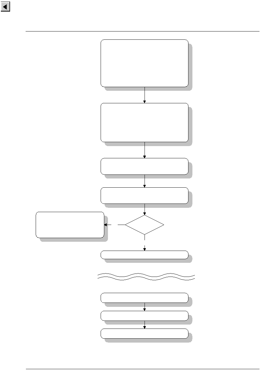
PRELIMINARY DATA SHEET
MSP 34x5G
Micronas
39
Fig. 3�2: Software flow diagram for a minimum demodulator setup for a European multistandard set applying the
Automatic Sound Select feature
:ULWH 6285&( 6(/(&7 6HWWLQJV
@hyr)
set loudspeaker Source Select to "Stereo or A"
set headphone Source Select to "Stereo or B"
set SCART_Out Source Select to "Stereo or A/B"
set Channel Matrix mode for all outputs to "Stereo"
:ULWH LQWR
67$1'$5' 6(/(&7 5HJLVWHU
(Start Automatic Standard Detection)
:ULWH 02'86 5HJLVWHU
:
@hyr
for the essential bits:
bd�2� �����������6hvp�Tq�Tryrp�2�
[1] = 1 Enable interrupt if STATUS changes
[8] = 0 ANA_IN1+ is selected
Define Preference for Automatic Standard
Detection:
[12] = 0 If 6.5 MHz, set SECAM-L
[14:13] = 3 Ignore 4.5 MHz carrier
Write FM/AM-Prescale
Write NICAM-Prescale
,Q FDVH RI LQWHUUXSW IURP
063 WR FRQWUROOHU
Read STATUS
Adjust TV-Display
If bilingual, adjust Source Select setting if required
Result = 0
?
set previous standard or
set standard manually according
picture information
yes
no
expecting interrupt from MSP
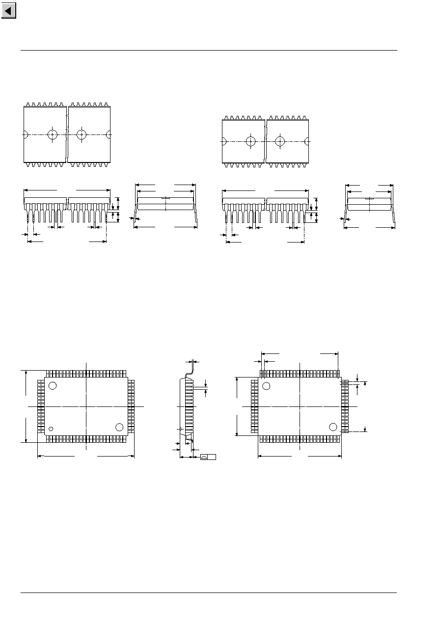
MSP 34x5G
PRELIMINARY DATA SHEET
40
Micronas
4. Specifications
4.1. Outline Dimensions
Fig. 4�1:
64-Pin Plastic Shrink Dual Inline Package
(PSDIP64)
Weight approximately 9.0 g
Dimensions in mm
Fig. 4�2:
52-Pin Plastic Shrink Dual Inline Package
(PSDIP52)
Weight approximately 5.5 g
Dimensions in mm
Fig. 4�3:
80-Pin Plastic Quad Flat Pack Package
(PQFP80)
Weight approximately 1.6 g
Dimensions in mm
1
32
33
64
57.7
�
0.1
0.8
�
0.2
3.8
�
0.1
3.2
�
0.2
1.778
1
�
0.05
31 x 1.778 = 55.1
�
0.1
0.48
�
0.06
20.3
�
0.5
0.28
�
0.06
18
�
0.05
19.3
�
0.1
SPGS703000-1(P64)/1E
1
26
27
52
47.0
�
0.1
0.6
�
0.2
4.0
�
0.1
2.8
�
0.2
1.778
1
�
0.05
25 x 1.778 = 44.4
�
0.1
0.48
�
0.06
SPGS703000-1(P52)/1E
16.3
�
1
0.28
�
0.06
14
�
0.1
15.6
�
0.1
15 x 0.8 = 12.0
0.1
�
0.8
0.8
41
64
24
1
65
80
40
25
0.1
3
�
0.2
SPGS705000-3(P80)/1E
23.2
0.15
�
17.2
0.15
�
20
0.1
�
14
0.1
�
23 x 0.8 = 18.4
0.1
�
0.17
0.04
�
0.37
0.04
�
1.3
0.05
�
2.7
0.1
�
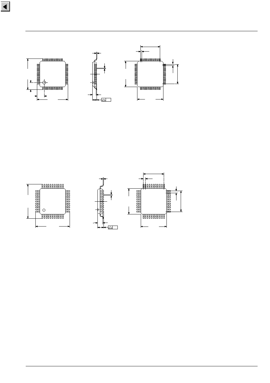
PRELIMINARY DATA SHEET
MSP 34x5G
Micronas
41
Fig. 4�4:
64-Pin Plastic Low-Profile Quad Flat Pack
(PLQFP64)
Weight approximately 0.35 g
Dimensions in mm
Fig. 4�5:
44-Pin Plastic Metric Quad Flat Pack
(PMQFP44)
Weight approximately 0.4 g
Dimensions in mm
10
0.1
�
1.75
1.75
49
64
1
16
17
32
33
48
D0025/3E
0.5
0.5
0.1
12
0.2
�
1.5
0.1
�
1.4
0.05
�
12
0.2
�
10
0.1
�
0.145
0.055
�
0.22
0.05
�
15 x 0.5 = 7.5
0.1
�
15 x 0.5 = 7.5
0.1
�
SPGS706000-5(P44)/1E
34
44
1
11
12
22
23
33
0.1
0.8
0.8
13.2
0.2
�
13.2
0.2
�
0.17
0.06
�
2.15
0.2
�
2.0
0.1
�
0.34
0.05
�
10
0.1
�
10
0.1
�
10 x 0.8 = 8
0.1
�
10 x 0.8 = 8
0.1
�

MSP 34x5G
PRELIMINARY DATA SHEET
42
Micronas
4.2. Pin Connections and Short Descriptions
NC = not connected; leave vacant
LV = if not used, leave vacant
DVSS: if not used, connect to DVSS
X = obligatory; connect as described in circuit diagram
AHVSS: connect to AHVSS
Pin No.
Pin Name
Type
Connection
(if not used)
Short Description
PQFP
80-pin
PLQFP
64-pin
PMQFP
44-pin
PSDIP
64-pin
PSDIP
52-pin
1
64
�
8
�
NC
LV
Not connected
2
1
12
9
7
I2C_CL
IN/OUT
X
I
2
C clock
3
2
13
10
8
I2C_DA
IN/OUT
X
I
2
C data
4
3
14
11
9
I2S_CL
LV
I
2
S clock
5
4
15
12
10
I2S_WS
LV
I
2
S word strobe
6
5
16
13
11
I2S_DA_OUT
LV
I
2
S data output
7
6
17
14
12
I2S_DA_IN1
LV
I
2
S1 data input
8
7
�
15
13
ADR_DA
LV
ADR data output
9
8
�
16
14
ADR_WS
LV
ADR word strobe
10
9
18
17
15
ADR_CL
LV
ADR clock
11
-
�
�
�
DVSUP
X
Digital power supply
+
5 V
12
-
�
�
�
DVSUP
X
Digital power supply
+
5 V
13
10
19
18
16
DVSUP
X
Digital power supply
+
5 V
14
-
20
�
�
DVSS
X
Digital ground
15
-
�
�
�
DVSS
X
Digital ground
16
11
�
19
17
DVSS
X
Digital ground
17
12
21
20
18
I2S_DA_IN2
LV
I
2
S2-data input
18
13
�
21
19
NC
LV
Not connected
19
14
�
22
�
NC
LV
Not connected
20
15
�
23
�
NC
LV
Not connected
21
16
22
24
20
RESETQ
IN
X
Power-on-reset
22
-
�
�
�
NC
LV
Not connected
23
-
�
�
�
NC
LV
Not connected
24
17
23
25
21
NC
LV
Not connected
25
18
24
26
22
NC
LV
Not connected
26
19
25
27
23
VREF2
X
Reference ground 2
high-voltage part

PRELIMINARY DATA SHEET
MSP 34x5G
Micronas
43
27
20
26
28
24
DACM_R
OUT
LV
Loudspeaker out, right
28
21
27
29
25
DACM_L
OUT
LV
Loudspeaker out, left
29
22
�
30
�
NC
LV
Not connected
30
23
�
31
26
NC
LV
Not connected
31
24
�
32
�
NC
LV
Not connected
32
-
�
�
�
NC
LV
Not connected
33
25
�
33
27
NC
LV
Not connected
34
26
28
34
28
NC
LV
Not connected
35
27
29
35
29
VREF1
X
Reference ground 1
high-voltage part
36
28
30
36
30
SC1_OUT_R
OUT
LV
SCART 1 output, right
37
29
31
37
31
SC1_OUT_L
OUT
LV
SCART 1 output, left
38
30
32
38
32
NC
LV
Not connected
39
31
33
39
33
AHVSUP
X
Analog power supply
8.0 V
40
32
34
40
34
CAPL_M
X
Volume capacitor MAIN
41
-
�
�
�
NC
LV
Not connected
42
-
�
�
�
NC
LV
Not connected
43
-
�
�
�
AHVSS
X
Analog ground
44
33
35
41
35
AHVSS
X
Analog ground
45
34
36
42
36
AGNDC
X
Analog reference voltage
high-voltage part
46
-
�
�
�
NC
LV
Not connected
47
35
�
43
�
NC
LV
Not connected
48
36
�
44
�
NC
LV
Not connected
49
37
�
45
�
NC
LV
Not connected
50
38
�
46
37
NC
LV
Not connected
51
39
�
47
38
NC
LV
Not connected
52
40
�
48
�
NC
AHVSS
Analog Shield Ground
53
41
37
49
39
SC2_IN_L
IN
LV
SCART 2 input, left
54
42
38
50
40
SC2_IN_R
IN
LV
SCART 2 input, right
55
43
39
51
�
ASG
AHVSS
Analog Shield Ground
56
44
40
52
41
SC1_IN_L
IN
LV
SCART 1 input, left
Pin No.
Pin Name
Type
Connection
(if not used)
Short Description
PQFP
80-pin
PLQFP
64-pin
PMQFP
44-pin
PSDIP
64-pin
PSDIP
52-pin
MSP 34x5G
PRELIMINARY DATA SHEET
44
Micronas
57
45
41
53
42
SC1_IN_R
IN
LV
SCART 1 input, right
58
46
42
54
43
VREFTOP
X
Reference voltage IF
A/D converter
59
-
�
�
�
NC
LV
Not connected
60
47
43
55
44
MONO_IN
IN
LV
Mono input
61
-
�
�
�
AVSS
X
Analog ground
62
48
44
56
45
AVSS
X
Analog ground
63
-
�
�
�
NC
LV
Not connected
64
-
�
�
�
NC
LV
Not connected
65
-
�
�
�
AVSUP
X
Analog power supply +5 V
66
49
1
57
46
AVSUP
X
Analog power supply +5 V
67
50
2
58
47
ANA_IN1
+
IN
LV
IF input 1
68
51
3
59
48
ANA_IN
-
IN
LV
IF common
69
52
�
60
49
NC
LV
Not connected
70
53
4
61
50
TESTEN
IN
X
Test pin
71
54
5
62
51
XTAL_IN
IN
X
Crystal oscillator
72
55
6
63
52
XTAL_OUT
OUT
X
Crystal oscillator
73
56
7
64
1
TP
LV
Test pin
74
57
�
1
2
NC
LV
Not connected
75
58
�
2
�
NC
LV
Not connected
76
59
�
3
�
NC
LV
Not connected
77
60
8
4
3
D_CTR_I/O_1
IN/OUT
LV
D_CTR_I/O_1
78
61
9
5
4
D_CTR_I/O_0
IN/OUT
LV
D_CTR_I/O_0
79
62
10
6
5
ADR_SEL
IN
X
I
2
C Bus address select
80
63
11
7
6
STANDBYQ
IN
X
Standby (low-active)
Pin No.
Pin Name
Type
Connection
(if not used)
Short Description
PQFP
80-pin
PLQFP
64-pin
PMQFP
44-pin
PSDIP
64-pin
PSDIP
52-pin

PRELIMINARY DATA SHEET
MSP 34x5G
Micronas
45
4.3. Pin Description
Pin numbers refer to the PQFP80 package
Pin 1, NC � Pin not connected
Pin 2, I2C_CL � I
2
C Clock Input/Output (Fig. 4�18)
Via this pin the I
2
C bus clock signal has to be supplied.
The signal can be pulled down by the MSP in case of
wait conditions.
Pin 3, I2C_DA � I
2
C Data Input/Output (Fig. 4�18)
Via this pin the I
2
C bus data is written to or read from
the MSP.
Pin 4, I2S_CL � I
2
S Clock Input/Output (Fig. 4�19)
Clock line for the I
2
S bus. In master mode, this line is
driven by the MSP; in slave mode, an external I
2
S
clock has to be supplied.
Pin 5, I2S_WS � I
2
S Word Strobe Input/Output
(Fig. 4�19)
Word strobe line for the I
2
S bus. In master mode, this
line is driven by the MSP; in slave mode, an external
I
2
S word strobe has to be supplied.
Pin 6, I2S_DA_OUT � I
2
S Data Output (Fig. 4�23)
Output of digital serial sound data of the MSP on the
I
2
S bus.
Pin 7, I2S_DA_IN1 � I
2
S Data Input 1 (Fig. 4�17)
First input of digital serial sound data to the MSP via
the I
2
S bus.
Pin 8, ADR_DA � ADR Bus Data Output (Fig. 4�23)
Output of digital serial data to the DRP 3510A via the
ADR bus.
Pin 9, ADR_WS � ADR Bus Word Strobe Output
(Fig. 4�23)
Word strobe output for the ADR bus.
Pin 10, ADR_CL � ADR Bus Clock Output (Fig. 4�23)
Clock line for the ADR bus.
Pins 11, 12, 13, DVSUP* � Digital Supply Voltage
Power supply for the digital circuitry of the MSP. Must
be connected to a +5-V power supply.
Pins 14, 15, 16, DVSS* � Digital Ground
Ground connection for the digital circuitry of the MSP
Pin 17, I2S_DA_IN2 � I
2
S Data Input 2 (Fig. 4�17)
Second input of digital serial sound data to the MSP
via the I
2
S bus.
Pins 18, 19, 20, NC � Pins not connected
Pin 21, RESETQ � Reset Input (Fig. 4�11)
In the steady state, high level is required. A low level
resets the MSP 34x0G.
Pins 22, 23, 24, 25, NC � Pins not connected
Pin 26, VREF2 � Reference Ground 2
Reference analog ground. This pin must be connected
separately to ground (AHVSS). VREF2 serves as a
clean ground and should be used as the reference for
analog connections to the loudspeaker and head-
phone outputs.
Pins 27, 28, DACM_R/L � Loudspeaker Outputs
(Fig. 4�21)
Output of the loudspeaker signal. A 1nF capacitor to
AHVSS must be connected to these pins. The DC off-
set on these pins depends on the selected loud-
speaker volume.
Pins 29, 30, 31, 32, 33, 34, NC � Pins not connected
Pin 35, VREF1 � Reference Ground 1
Reference analog ground. This pin must be connected
separately to ground (AHVSS). VREF1 serves as a
clean ground and should be used as the reference for
analog connections to the SCART outputs.
Pins 36, 37, SC1_OUT_R/L � SCART1 Outputs
(Fig. 4�22)
Output of the SCART1 signal. Connections to these
pins must use a 100 ohm series resistor and are
intended to be AC coupled.
Pin 38, NC � Pin not connected
Pin 39, AHVSUP* � Analog Power Supply High Voltage
Power is supplied via this pin for the analog circuitry of
the MSP (except IF input). This pin must be connected
to the +8V supply.
Pin 40, CAPLM � Volume Capacitor Loudspeakers
(Fig. 4�24)
A 10
�
F capacitor to AHVSUP must be connected to
this pin. It serves as smoothing filter for loudspeaker
volume changes in order to suppress audible plops.
The value of the capacitor can be lowered to 1
�
F if
faster response is required. The area encircled by the
trace lines should be minimized, keep traces as short
as possible. This input is sensitive for magnetic induc-
tion.
Pins 41, 42, NC � Pins not connected.
Pins 43, 44, AHVSS* � Ground for Analog Power Sup-
ply High Voltage
Ground connection for the analog circuitry of the MSP
(except IF input).
Pins 45, AGNDC � Internal Analog Reference Voltage
This pin serves as the internal ground connection for
the analog circuitry (except IF input). It must be con-
nected to the VREF pins with a 3.3
�
F and a 100 nF
capacitor in parallel. This pins shows a DC level of typ-
ically 3.73 V.

MSP 34x5G
PRELIMINARY DATA SHEET
46
Micronas
Pin 46, 47, 48, 49, 50, 51 NC � Pins not connected.
Pin 52, ASG � Analog Shield Ground
Analog ground (AHVSS) should be connected to this
pin to reduce cross coupling between SCART inputs.
Pins 53, 54, SC2_IN_L/R � SCART2 Inputs
(Fig. 4�14)
The analog input signal for SCART2 is fed to this pin.
Analog input connection must be AC coupled.
Pin 55, ASG � Analog Shield Ground
Analog ground (AHVSS) should be connected to this
pin to reduce cross coupling between SCART inputs.
Pins 56, 57, SC1_IN_L/R � SCART1 Inputs
(Fig. 4�14)
The analog input signal for SCART1 is fed to this pin.
Analog input connection must be AC coupled.
Pin 58, VREFTOP � Reference Voltage IF AD Con-
verter (Fig. 4�15)
Via this pin, the reference voltage for the IF AD con-
verter is decoupled. It must be connected to AVSS
pins with a 10
�
F and a 100nF capacitor in parallel.
Traces must be kept short.
Pin 59, NC � Pin not connected
Pin 60, MONO_IN � Mono Input (Fig. 4�14)
The analog mono input signal is fed to this pin. Analog
input connection must be AC coupled.
Pins 61, 62, AVSS* � Ground for Analog Power Supply
Voltage
Ground connection for the analog IF input circuitry of
the MSP.
Pins 63, 64, NC � Pins not connected
Pins 65, 66, AVSUP* � Analog Power Supply Voltage
Power is supplied via this pin for the analog IF input cir-
cuitry of the MSP. This pin must be connected to the
+5 V supply.
Pin 67, ANA_IN1+ � IF Input 1 (Fig. 4�15)
The analog sound if signal is supplied to this pin.
Inputs must be AC coupled. This pin is designed as
symmetrical input: ANA_IN1+ is internally connected
to one input of a symmetrical op amp, ANA_IN
-
to the
other.
Pin 68, ANA_IN
-
� IF Common (Fig. 4�15)
This pin serves as a common reference for ANA_IN1/
2+ inputs.
Pin 69, NC � Pin not connected
Pin 70, TESTEN � Test Enable Pin (Fig. 4�12)
This pin enables factory test modes. For normal opera-
tion it must be connected to ground.
Pins71, 72, XTAL_IN, XTAL_OUT � Crystal Input and
Output Pins (Fig. 4�20)
These pins are connected to an 18.432 MHz crystal
oscillator which is digitally tuned by integrated shunt
capacitances. An external clock can be fed into
XTAL_IN. The audio clock output signal AUD_CL_OUT
is derived form the oscillator. External capacitors at
each crystal pin to ground (AVSS) are required. It
should be verified by layout, that no supply current for
the digital circuitry is flowing through the ground con-
nection point.
Pin 73, TP � Test pin
Pins 74, 75, 76, NC � Pins not connected
Pins 77, 78, D_CTR_I/O_1/0 � Digital Control Input/
Output Pins (Fig. 4�19)
General purpose input/output pins. Pin D_CTR_I/O_1
can be used as an interrupt request pin to the control-
ler.
Pin 79, ADR_SEL � I
2
C Bus Address Select
(Fig. 4�16)
By means of this pin, one of 3 device addresses for the
MSP can be selected. The pin can be connected to
ground (I
2
C device addresses 80/81
hex
), to +5V supply
(84/85
hex
) or left open (88/89
hex
).
Pin 80, STANDBYQ � Standby
In normal operation, this pin must be high. If the
MSP 34x5G is switched off by first pulling STANDBYQ
low and then (after >1
�
s delay) switching off DVSUP
and AVSUP, but keeping AHVSUP (`Standby'-mode),
the SCART switches maintain their position and func-
tion.
* Application Note:
All ground pins should be connected to one low-resis-
tive ground plane. All supply pins should be connected
separately with short and low-resistive lines to the
power supply. Decoupling capacitors from DVSUP to
DVSS, AVSUP to AVSS, and AHVSUP to AHVSS are
recommended as closely as possible to these pins.
Decoupling of DVSUP and DVSS is most important.
We recommend using more than one capacitor. By
choosing different values, the frequency range of
active decoupling can be extended. In our application
boards we use: 220 pF, 470 pF, 1.5 nF, and 10
�
F. The
capacitor with the lowest value should be placed near-
est to the DVSUP and DVSS pins.
The ASG pins should be connected as closely as pos-
sible to the MSP ground. If they are lead with the
SCART-inputs as shielding lines, they should not be
connected to ground at the SCART connector.
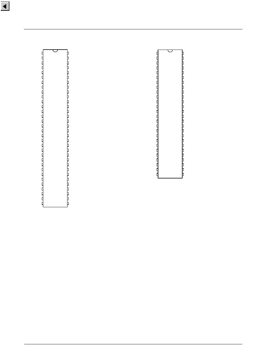
PRELIMINARY DATA SHEET
MSP 34x5G
Micronas
47
4.4. Pin Configurations
Fig. 4�6: PSDIP64 package
Fig. 4�7: PSDIP52 package
1
NC
2
NC
3
NC
4
D_CTR_I/O_1
5
D_CTR_I/O_0
6
ADR_SEL
7
STANDBYQ
8
NC
9
I2C_CL
10
I2C_DA
11
I2S_CL
12
I2S_WS
13
I2S_DA_OUT
14
I2S_DA_IN1
15
ADR_DA
16
ADR_WS
TP
64
XTAL_OUT
63
XTAL_IN
62
TESTEN
61
NC
60
ANA_IN
-
59
ANA_IN1+
58
AVSUP
57
AVSS
56
MONO_IN
55
VREFTOP
54
SC1_IN_R
53
SC1_IN_L
52
ASG
51
SC2_IN_R
50
SC2_IN_L
49
17
ADR_CL
18
DVSUP
19
DVSS
20
I2S_DA_IN2
21
NC
22
NC
23
NC
24
RESETQ
25
NC
26
NC
NC
48
NC
47
NC
46
NC
45
NC
44
NC
43
AGNDC
42
AHVSS
41
CAPL_M
40
AHVSUP
39
M
SP 34x
5G
VREF2
DACM_R
DACM_L
NC
NC
NC
38
37
36
35
34
33
27
28
29
30
31
32
NC
SC1_OUT_L
SC1_OUT_R
VREF1
NC
NC
1
2
3
4
5
6
7
8
9
10
11
12
13
14
15
16
17
18
19
20
21
22
23
24
25
26
52
51
50
49
48
47
46
45
44
43
42
41
40
39
38
37
36
35
34
33
32
31
30
29
28
27
TP
NC
D_CTR_I/O_1
D_CTR_I/O_0
ADR_SEL
STANDBYQ
I2C_CL
I2C_DA
I2S_CL
I2S_WS
I2S_DA_OUT
I2S_DA_IN1
ADR_DA
ADR_WS
ADR_CL
DVSUP
XTAL_OUT
XTAL_IN
TESTEN
NC
ANA_IN
-
ANA_IN1
+
AVSUP
AVSS
MONO_IN
VREFTOP
SC1_IN_R
SC1_IN_L
SC2_IN_R
SC2_IN_L
NC
NC
DVSS
I2S_DA_IN2
NC
RESETQ
NC
NC
VERF2
DACM_R
DACM_L
NC
AGNDC
AHVSS
CAPL_M
AHVSUP
NC
SC1_OUT_L
SC1_OUT_R
VREF1
NC
NC
M
S
P
34
x5
G

MSP 34x5G
PRELIMINARY DATA SHEET
48
Micronas
Fig. 4�8: PQFP80 package
65
66
67
68
69
70
71
72
73
74
75
76
77
78
79
80
40
39
38
37
36
35
34
33
32
31
30
29
28
27
26
25
1
2
3
4
5
6
7
8
9
10 11 12 13 14 15 16 17 18 19 20 21 22 23 24
64 63 62 61 60 59 58 57 56 55 54 53 52 51 50 49 48 47 46 45 44 43 42 41
AVSUP
AVSUP
ANA_IN1
+
ANA_IN
-
NC
TESTEN
XTAL_IN
XTAL_OUT
TP
NC
NC
NC
D_CTR_I/O_1
D_CTR_I/O_0
ADR_SEL
STANDBYQ
CAPL_M
AHVSUP
NC
SC1_OUT_L
SC1_OUT_R
VREF1
NC
NC
NC
NC
NC
NC
DACM_L
DACM_R
VREF2
NC
NC
AVSS
AVSS
MONO_IN
NC
VREFTOP
SC1_IN_R
SC1_IN_L
ASG
NC
SC2_IN_R
SC2_IN_L
ASG
NC
NC
NC
NC
NC
NC
AGNDC
AHVSS
AHVSS
NC
NC
I2C_CL
I2C_DA
I2S_CL
I2S_WS
I2S_DA_OUT
I2S_DA_IN1
ADR_DA
ADR_WS
ADR_CL
NC
DVSUP
DVSUP
DVSUP
DVSS
DVSS
DVSS
I2S_DA_IN2
NC
NC
NC
RESETQ
NC
NC
NC
MSP 34x5G

PRELIMINARY DATA SHEET
MSP 34x5G
Micronas
49
Fig. 4�9: PLQFP64 package
AVSUP
ANA_IN1+
ANA_IN
-
NC
TESTEN
XTAL_IN
XTAL_OUT
TP
NC
NC
NC
D_CTR_I/OUT1
D_CTR_I/OUT0
ADR_SEL
STANDBYQ
NC
CAPL_M
AHVSUP
NC
SC1_OUT_L
SC1_OUT_R
VREF1
NC
NC
NC
NC
NC
DACM_L
DACM_R
VREF2
NC
NC
MONO_IN
VREFTOP
SC1_IN_R
SC1_IN_L
ASG
SC2_IN_R
SC2_IN_L
AVSS
ASG
NC
NC
NC
NC
NC
AGNDC
AHVSS
I2C_DA
I2S_CL
I2S_WS
I2S_DA_OUT
I2S_DA_IN1
ADR_DA
ADR_WS
I2C_CL
ADR_CL
DVSUP
DVSS
I2S_DA_IN2
NC
NC
NC
RESETQ
MSP 34x5G
49
50
51
52
53
54
55
56
57
58
59
60
61
62
63
64
32
31
30
29
28
27
26
25
24
23
22
21
20
19
18
17
1
2
3
4
5
6
7
8
9
10 11 12 13 14 15 16
48 47 46 45 44 43 42 41 40 39 38 37 36 35 34 33
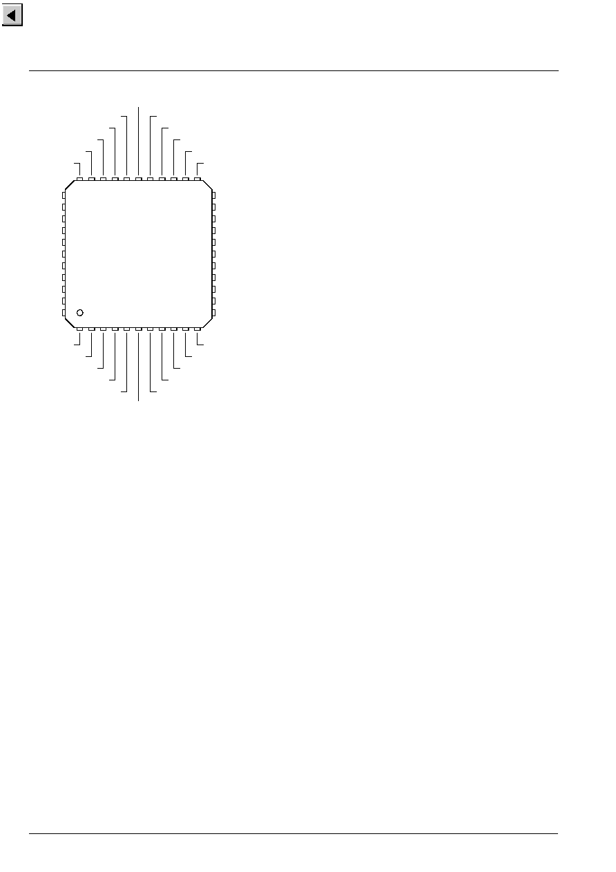
MSP 34x5G
PRELIMINARY DATA SHEET
50
Micronas
Fig. 4�10: PMQFP44 package
CAPL_M
AHVSS
AGNDC
SC2_IN_L
SC2_IN_R
ASG
SC1_IN_L
SC1_IN_R
VREFTOP
MONO_IN
AVSS
RESETQ
I2S_DA_IN2
DVSS
DVSUP
ADR_CL
I2S_DA_IN1
I2S_DA_OUT
I2S_WS
I2S_CL
I2C_DA
I2C_CL
NC
SC1_OUT_L
SC1_OUT_R
VREF1
NC
AHVSUP
DACM_L
DACM_R
VREF2
NC
NC
ANA_IN1
+
ANA_IN
-
TESTEN
XTAL_IN
XTAL_OUT
AVSUP
TP
D_CTR_I/O1
D_CTR_I/O0
ADR_SEL
STANDBYQ
MSP 34x5G
34
35
36
37
38
39
40
41
42
43
44
22
21
20
19
18
17
16
15
14
13
12
1
2
3
4
5
6
7
8
9
10 11
33 32 31 30 29 28 27 26 25 24 23

PRELIMINARY DATA SHEET
MSP 34x5G
Micronas
51
4.5. Pin Circuits
Fig. 4�11: Input Pin: RESETQ
Fig. 4�12: Input Pin TESTEN
Fig. 4�13: Input Pin MONO_IN
Fig. 4�14: Input Pins: SC2-1_IN_L/R
Fig. 4�15: Input Pins:
VREFTOP, ANA_IN1+, ANA_IN
-
Fig. 4�16: Input Pin: ADR_SEL
Fig. 4�17: Input Pins: I2S_DA_IN1/2, STANDBYQ
DVSS
>300 k
AVSUP
200 k
3.75 V
24 k
3.75 V
40 k
D
A
ANA_IN1+
VREFTOP
ANA_IN1
-
ADR_SEL
GND
DVSUP
23 k
23 k

MSP 34x5G
PRELIMINARY DATA SHEET
52
Micronas
Fig. 4�18: Input/Output Pins: I2C_CL, I2C_DA
Fig. 4�19: Input/Output Pins:
I2S_CL, I2S_WS, D_CTR_I/O_1, D_CTR_I/O_0
Fig. 4�20: Input/Output Pins
XTAL_IN, XTAL_OUT
Fig. 4�21: Output Pins: DACM_R/L
Fig. 4�22: Output Pins: SC_1_OUT_R/L
Fig. 4�23: Output Pins:
I2S_DA_OUT, ADR_DA, ADR_WS, ADR_CL
Fig. 4�24: Capacitor Pin: CAPL_M
Fig. 4�25: Pin: AGNDC
N
GND
DVSUP
P
N
GND
3
-
30 pF
500 k
3
-
30 pF
P
N
AHVSUP
0...1.2 mA
3.3 k
26 pF
120 k
300
3.75 V
DVSUP
P
N
GND
0...2 V
3.75 V
125 k
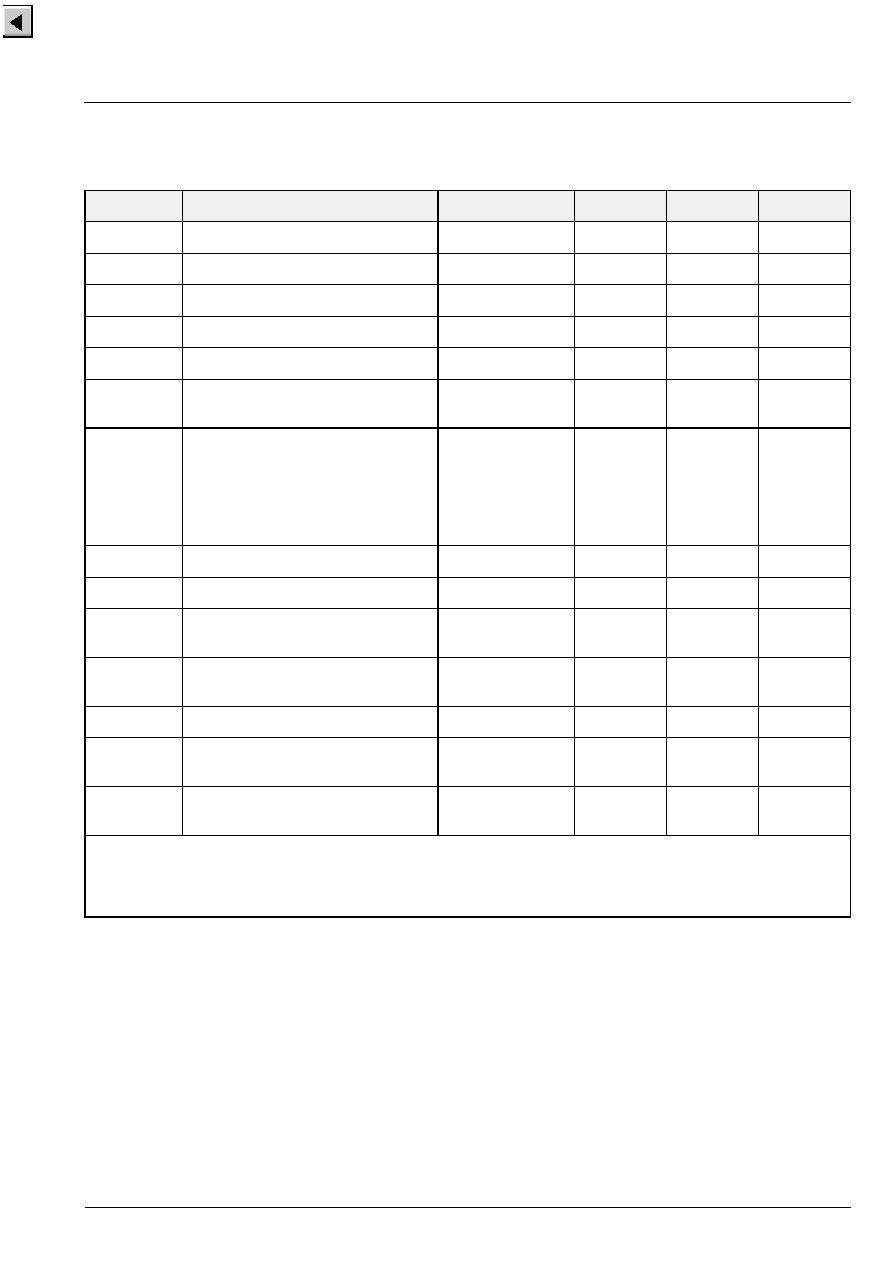
PRELIMINARY DATA SHEET
MSP 34x5G
Micronas
53
4.6. Electrical Characteristics
4.6.1. Absolute Maximum Ratings
Stresses beyond those listed in the "Absolute Maximum Ratings" may cause permanent damage to the device. This
is a stress rating only. Functional operation of the device at these or any other conditions beyond those indicated in
the "Recommended Operating Conditions/Characteristics" of this specification is not implied. Exposure to absolute
maximum ratings conditions for extended periods may affect device reliability.
Symbol
Parameter
Pin Name
Min.
Max.
Unit
T
A
Ambient Operating Temperature
�
0
70
�
C
T
S
Storage Temperature
�
-
40
125
�
C
V
SUP1
First Supply Voltage
AHVSUP
-
0.3
9.0
V
V
SUP2
Second Supply Voltage
DVSUP
-
0.3
6.0
V
V
SUP3
Third Supply Voltage
AVSUP
-
0.3
6.0
V
dV
SUP23
Voltage between AVSUP
and DVSUP
AVSUP,
DVSUP
-
0.5
0.5
V
P
TOT
Package Power Dissipation
PSDIP64
PSDIP52
PQFP80
PLQFP64
PMQFP44
AHVSUP,
DVSUP,
AVSUP
1300
1200
1000
960
960
mW
mW
mW
mW
mW
V
Idig
Input Voltage, all Digital Inputs
-
0.3
V
SUP2
+0.3
V
I
Idig
Input Current, all Digital Pins
�
-
20
+20
mA
1)
V
Iana
Input Voltage, all Analog Inputs
SCn_IN_s,
2)
MONO_IN
-
0.3
V
SUP1
+0.3
V
I
Iana
Input Current, all Analog Inputs
SCn_IN_s,
2)
MONO_IN
-
5
+5
mA
1)
I
Oana
Output Current, all SCART Outputs
SC1_OUT_s
2)
3)
,
4)
3)
,
4)
I
Oana
Output Current, all Analog Outputs
except SCART Outputs
DACM_s
2)
3)
3)
I
Cana
Output Current, other pins
connected to capacitors
CAPL_M,
AGNDC
3)
3)
1)
positive value means current flowing into the circuit
2)
"n" means "1" or "2", "s" means "L" or "R"
3)
The Analog Outputs are short-circuit proof with respect to First Supply Voltage and Ground.
4)
Total chip power dissipation must not exceed absolute maximum rating.
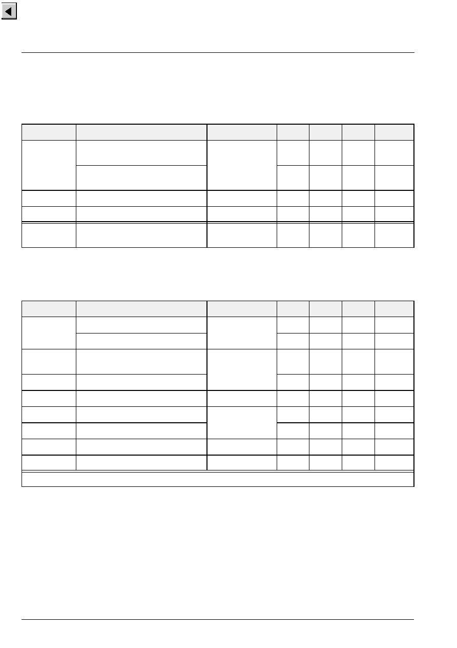
MSP 34x5G
PRELIMINARY DATA SHEET
54
Micronas
4.6.2. Recommended Operating Conditions
at T
A
= 0 to 70
�
C
4.6.2.1. General Recommended Operating Conditions
4.6.2.2. Analog Input and Output Recommendations
Symbol
Parameter
Pin Name
Min.
Typ.
Max.
Unit
V
SUP1
First Supply Voltage
(AHVSUP = 8 V)
AHVSUP
7.6
8.0
8.7
V
First Supply Voltage
(AHVSUP = 5V)
4.75
5.0
5.25
V
V
SUP2
Second Supply Voltage
DVSUP
4.75
5.0
5.25
V
V
SUP3
Third Supply Voltage
AVSUP
4.75
5.0
5.25
V
t
STBYQ1
STANDBYQ Setup Time before
Turn-off of Second Supply Voltage
STANDBYQ,
DVSUP
1
�
s
Symbol
Parameter
Pin Name
Min.
Typ.
Max.
Unit
C
AGNDC
AGNDC-Filter-Capacitor
AGNDC
-
20%
3.3
�
F
Ceramic Capacitor in Parallel
-
20%
100
nF
C
inSC
DC-Decoupling Capacitor in front of
SCART Inputs
SCn_IN_s
1)
-
20%
330
nF
V
inSC
SCART Input Level
2.0
V
RMS
V
inMONO
Input Level, Mono Input
MONO_IN
2.0
V
RMS
R
LSC
SCART Load Resistance
SC1_OUT_s
1)
10
k
C
LSC
SCART Load Capacitance
6.0
nF
C
VMA
Main Volume Capacitor
CAPL_M
10
�
F
C
FMA
Main Filter Capacitor
DACM_s
1)
-
10%
1
+
10%
nF
1)
"n" means "1" or "2", "s" means "L" or "R"

PRELIMINARY DATA SHEET
MSP 34x5G
Micronas
55
4.6.2.3. Recommendations for Analog Sound IF Input Signal
Symbol
Parameter
Pin Name
Min.
Typ.
Max.
Unit
C
VREFTOP
VREFTOP-Filter-Capacitor
VREFTOP
-
20%
10
�
F
Ceramic Capacitor in Parallel
-
20%
100
nF
F
IF_FMTV
Analog Input Frequency Range
for TV applications
ANA_IN1+,
ANA_IN
-
0
9
MHz
F
IF_FMRADIO
Analog Input Frequency for
FM-Radio Applications
10.7
MHz
V
IF_FM
Analog Input Range FM/NICAM
0.1
0.8
3
V
pp
V
IF_AM
Analog Input Range AM/NICAM
0.1
0.45
0.8
V
pp
R
FMNI
Ratio: NICAM Carrier/FM Carrier
(unmodulated carriers)
BG:
I:
-
20
-
23
-
7
-
10
0
0
dB
dB
R
AMNI
Ratio: NICAM Carrier/AM Carrier
(unmodulated carriers)
-
25
-
11
0
dB
R
FM
Ratio: FM-Main/FM-Sub Satellite
7
dB
R
FM1/FM2
Ratio: FM1/FM2
German FM-System
7
dB
R
FC
Ratio: Main FM Carrier/
Color Carrier
15
�
�
dB
R
FV
Ratio: Main FM Carrier/
Luma Components
15
�
�
dB
PR
IF
Passband Ripple
�
�
�
2
dB
SUP
HF
Suppression of Spectrum
above 9.0 MHz (not for FM Radio)
15
�
dB
FM
MAX
Maximum FM-Deviation (approx.)
normal mode
HDEV2: high deviation mode
HDEV3: very high deviation mode
�
180
�
360
�
540
kHz
kHz
kHz
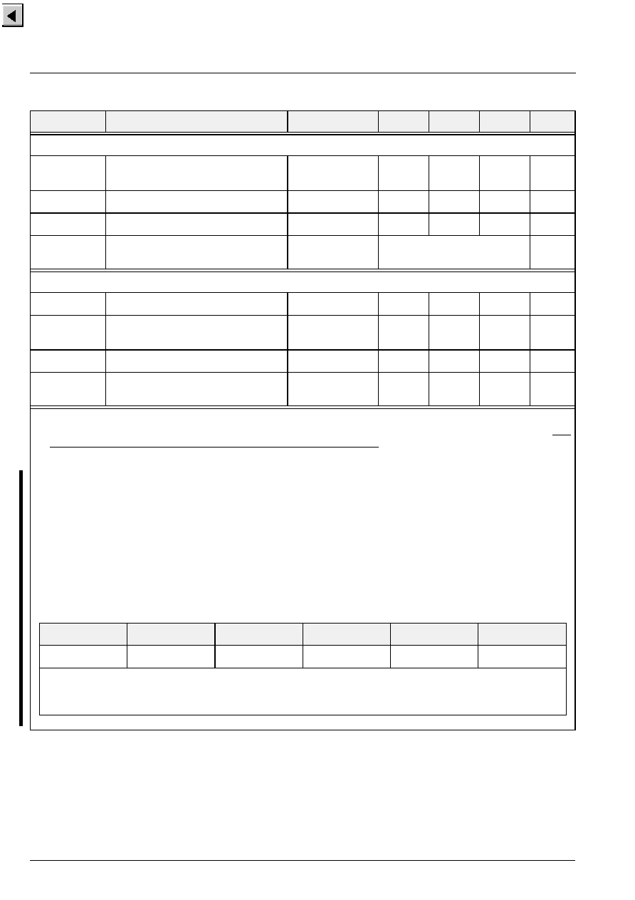
MSP 34x5G
PRELIMINARY DATA SHEET
56
Micronas
4.6.2.4. Crystal Recommendations
Symbol
Parameter
Pin Name
Min.
Typ.
Max.
Unit
General Crystal Recommendations
f
P
Crystal Parallel Resonance Fre-
quency at 12 pF Load Capacitance
18.432
MHz
R
R
Crystal Series Resistance
8
25
C
0
Crystal Shunt (Parallel) Capacitance
6.2
7.0
pF
C
L
External Load Capacitance
1)
XTAL_IN,
XTAL_OUT
PSDIP
approx. 1.5
P(L,M)QFPapprox. 3.3
pF
pF
Crystal Recommendations for Master-Slave Applications
(MSP-clock must perform synchronization to I
2
S clock)
f
TOL
Accuracy of Adjustment
-
20
+
20
ppm
D
TEM
Frequency Variation
versus Temperature
-
20
+
20
ppm
C
1
Motional (Dynamic) Capacitance
19
24
fF
f
CL
Required Open Loop Clock
Frequency (T
amb
= 25
�
C)
18.431
18.433
MHz
1)
External capacitors at each crystal pin to ground are required. They are necessary to tune the open-loop fre-
quency of the internal PLL and to stabilize the frequency in closed-loop operation. Due to different layouts, the
accurate capacitor value should be determined with the customer PCB. The suggested values (1.5...3.3 pF) are
figures based on experience and should serve as "start value".
To adjust the capacitor value, reset the MSP and transfer only the following I
2
C-protocol:
<80 10 00 20 00 60>.
Measure the frequency at pin ADR_CL. Measurement at XTAL_IN/OUT pins is not possible. Change the
capacitor value until the frequency matches 18.432/3 = 6.144 MHz as closely as possible. The higher the
capacity, the lower the resulting clock frequency.
Note: To minimize adjustment tolerances for all MSP-generations, it is strongly recommended to use the so-
called MSP-XTAL-REF ICs (available in all packages) for the capacitor adjustment. Since all MSP-XTAL-REF ICs
do have an AUD_CL_OUT-pin with the 18.432 MHz signal, this pin should be used for the capacitor adjustment
instead of the ADR_CL-pin. After the reset, no I
2
C-protocol should be transmitted. The AUD_CL_OUT-signal is
available at the following pins:
PLCC68
PSDIP64
PSDIP52
PQFP80
PLQFP64
PMQFP44
2)
pin 18
pin 1
pin 2
pin 74
pin 57
pin 8
2)
For the MSP-XTAL-REF IC, the PMQFP44 pin functionality of the D_CTR_I/O1-pin has been changed to
the Audio_Clock_Out signal. If D_CTR_I/O1 is used in the customer application, this pin must be left open for
the adjustment procedure.

PRELIMINARY DATA SHEET
MSP 34x5G
Micronas
57
Crystal Recommendations for FM / NICAM Applications
(No MSP-clock synchronization to I
2
S clock possible)
f
TOL
Accuracy of Adjustment
-
30
+
30
ppm
D
TEM
Frequency Variation
versus Temperature
-
30
+
30
ppm
C
1
Motional (Dynamic) Capacitance
15
fF
f
CL
Required Open Loop Clock
Frequency (T
amb
= 25
�
C)
18.4305
18.4335
MHz
Crystal Recommendations for all analog FM/AM Applications
(No MSP-clock synchronization to I
2
S clock possible)
f
TOL
Accuracy of Adjustment
-
100
+
100
ppm
D
TEM
Frequency Variation
versus Temperature
-
50
+
50
ppm
f
CL
Required Open Loop Clock
Frequency (T
amb
= 25
�
C)
18.429
18.435
MHz
Amplitude Recommendation for Operation with External Clock Input (C
load
after reset typ. 22 pF)
V
XCA
External Clock Amplitude
XTAL_IN
0.7
V
pp
Symbol
Parameter
Pin Name
Min.
Typ.
Max.
Unit
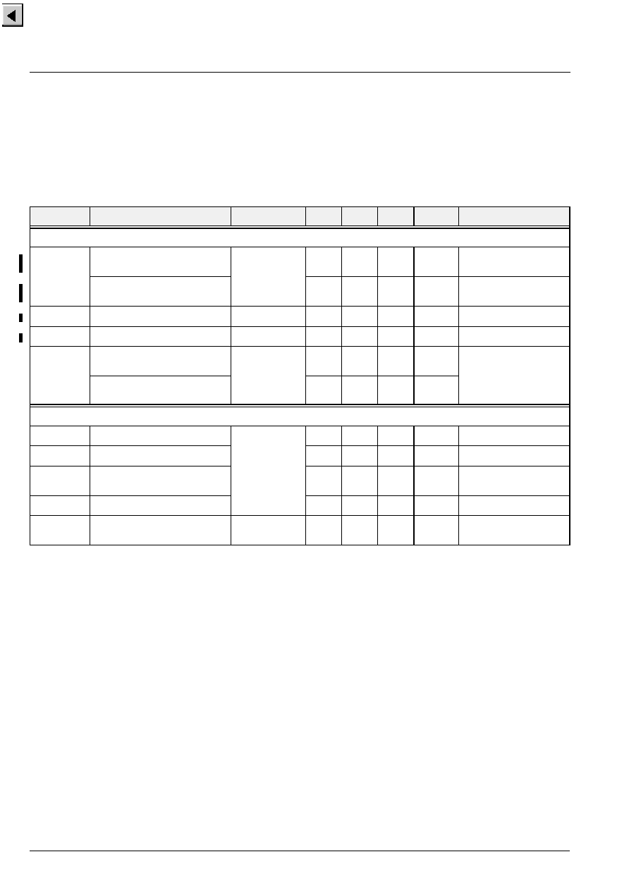
MSP 34x5G
PRELIMINARY DATA SHEET
58
Micronas
4.6.3. Characteristics
at T
A
= 0 to 70
�
C, f
CLOCK
= 18.432 MHz, V
SUP1
= 7.6 to 8.7 V, V
SUP2
= 4.75 to 5.25 V for min./max. values
at T
A
= 60
�
C, f
CLOCK
= 18.432 MHz, V
SUP1
= 8 V, V
SUP2
= 5 V for typical values,
T
J
= Junction Temperature
MAIN (M) = Loudspeaker Channel
4.6.3.1. General Characteristics
Symbol
Parameter
Pin Name
Min.
Typ.
Max.
Unit
Test Conditions
Supply
I
SUP1A
First Supply Current (active)
(AHVSUP = 8 V)
AHVSUP
17
11
25
16
mA
mA
Vol. Main and Aux = 0 dB
Vol. Main and Aux = -30dB
First Supply Current (active)
(AHVSUP = 5 V)
11
8
17
11
mA
mA
Vol. Main and Aux = 0 dB
Vol. Main and Aux = -30 dB
I
SUP2A
Second Supply Current (active)
DVSUP
55
70
mA
I
SUP3A
Third Supply Current (active)
AVSUP
30
38
mA
I
SUP1S
First Supply Current
(AHVSUP = 8 V)
AHVSUP
5.6
7.7
mA
STANDBYQ = low
First Supply Current
(AHVSUP = 5 V)
3.7
5.1
mA
Clock
f
CLOCK
Clock Input Frequency
XTAL_IN
18.432
MHz
D
CLOCK
Clock High to Low Ratio
45
55
%
t
JITTER
Clock Jitter
(verification not
provided in production test)
50
ps
V
xtalDC
DC-Voltage Oscillator
2.5
V
t
Startup
Oscillator
Startup Time
at
VDD Slew-rate of 1 V/1
�
s
XTAL_IN,
XTAL_OUT
0.4
2
ms
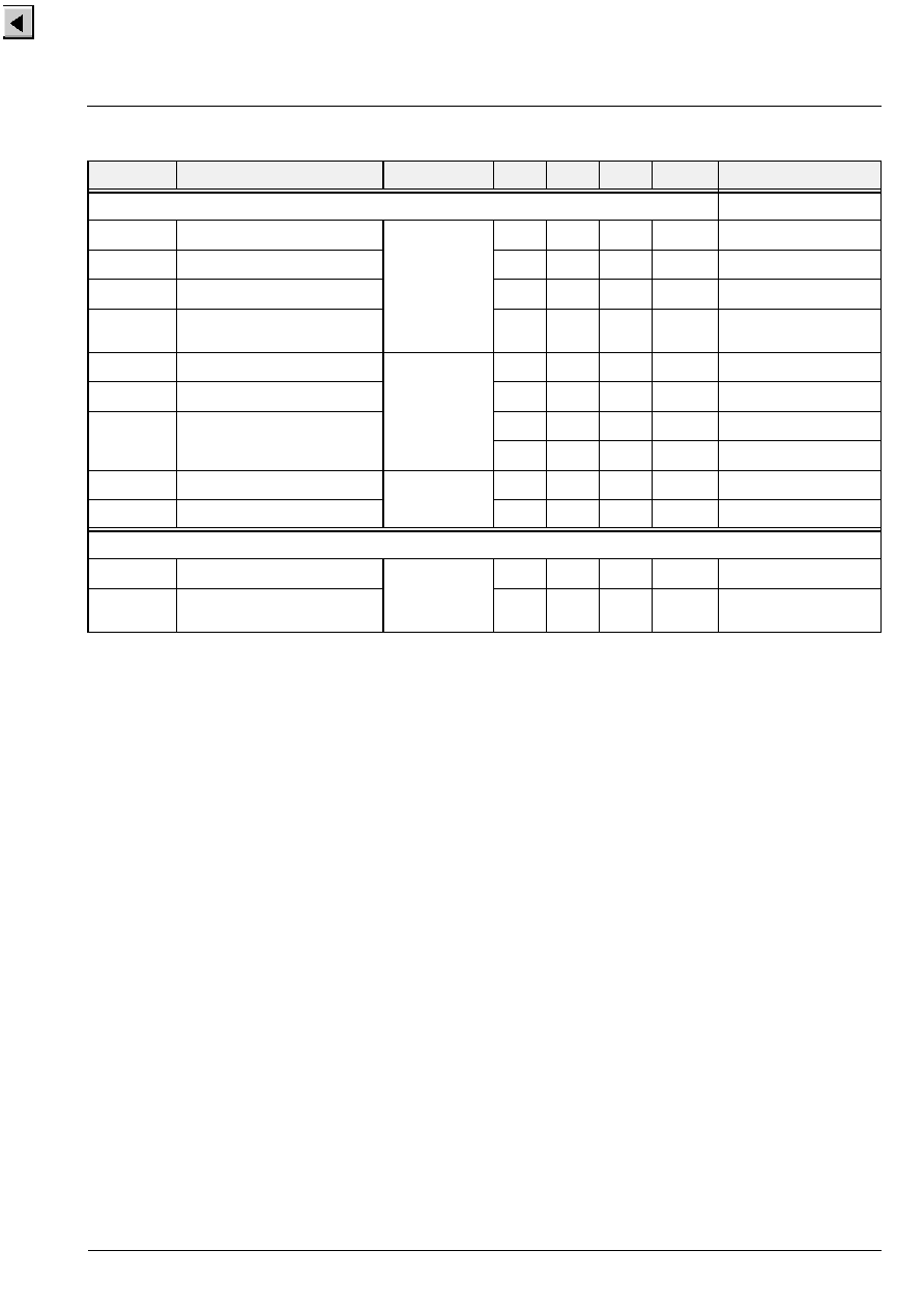
PRELIMINARY DATA SHEET
MSP 34x5G
Micronas
59
4.6.3.2. Digital Inputs, Digital Outputs
Symbol
Parameter
Pin Name
Min.
Typ.
Max.
Unit
Test Conditions
Digital Input Levels
V
DIGIL
Digital Input Low Voltage
STANDBYQ
D_CTR_I/O_0/1
0.2
V
SUP2
V
DIGIH
Digital Input High Voltage
0.5
V
SUP2
Z
DIGI
Input Impedance
5
pF
I
DLEAK
Digital Input Leakage Current
-
1
1
�
A
0 V < U
INPUT
< DVSUP
D_CTR_I/O_0/1: tri-state
V
DIGIL
Digital Input Low Voltage
ADR_SEL
0.2
V
SUP2
V
DIGIH
Digital Input High Voltage
0.8
V
SUP2
I
ADRSEL
Input Current Address Select Pin
-
500
-
220
�
A
U
ADR_SEL
= DVSS
220
500
�
A
U
ADR_SEL
= DVSUP
Z
TESTEN
Input Capacitance
TESTEN
5
pF
I
TESTEN
Input Low Current
-
60
�
A
U
TESTEN
= AVSS
Digital Output Levels
V
DCTROL
Digital Output Low Voltage
D_CTR_I/O_0
D_CTR_I/O_1
0.4
V
IDDCTR = 1 mA
V
DCTROH
Digital Output High Voltage
V
SUP2
-
0.3
V
IDDCTR =
-
1 mA
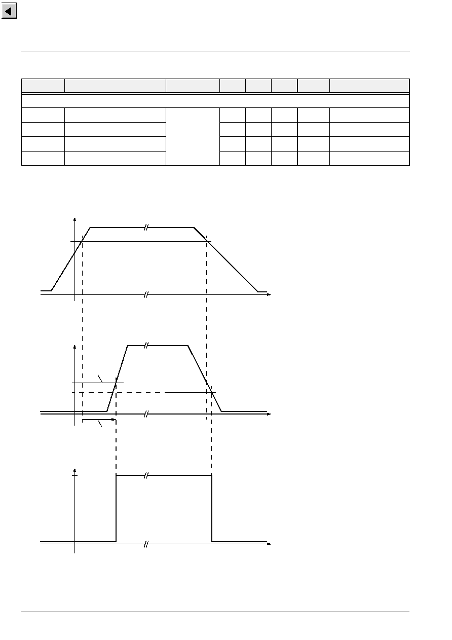
MSP 34x5G
PRELIMINARY DATA SHEET
60
Micronas
4.6.3.3. Reset Input and Power-Up
Fig. 4�26: Power-up sequence
Symbol
Parameter
Pin Name
Min.
Typ.
Max.
Unit
Test Conditions
RESETQ Input Levels
V
RHL
Reset High-Low Transition Voltage
RESETQ
0.3
0.4
V
SUP2
V
RLH
Reset Low-High Transition Voltage
0.45
0.55
V
SUP2
Z
RES
Input Capacitance
5
pF
I
RES
Input High Current
20
�
A
U
RESETQ
= DVSUP
4.5 V
Internal
Reset
t/ms
RESETQ
AVSUP
DVSUP
High
Low
t/ms
t/ms
Note: The reset should
not reach high level
before the oscillator has
started. This requires a
reset delay of >2 ms
0.45 x DVSUP means
2.25 Volt with
DVSUP = 5.0 V
0.3...0.4
�
DVSUP
0.45
�
DVSUP
High-to-Low
Threshold
Low-to-High
Threshold
Reset Delay
>2 ms
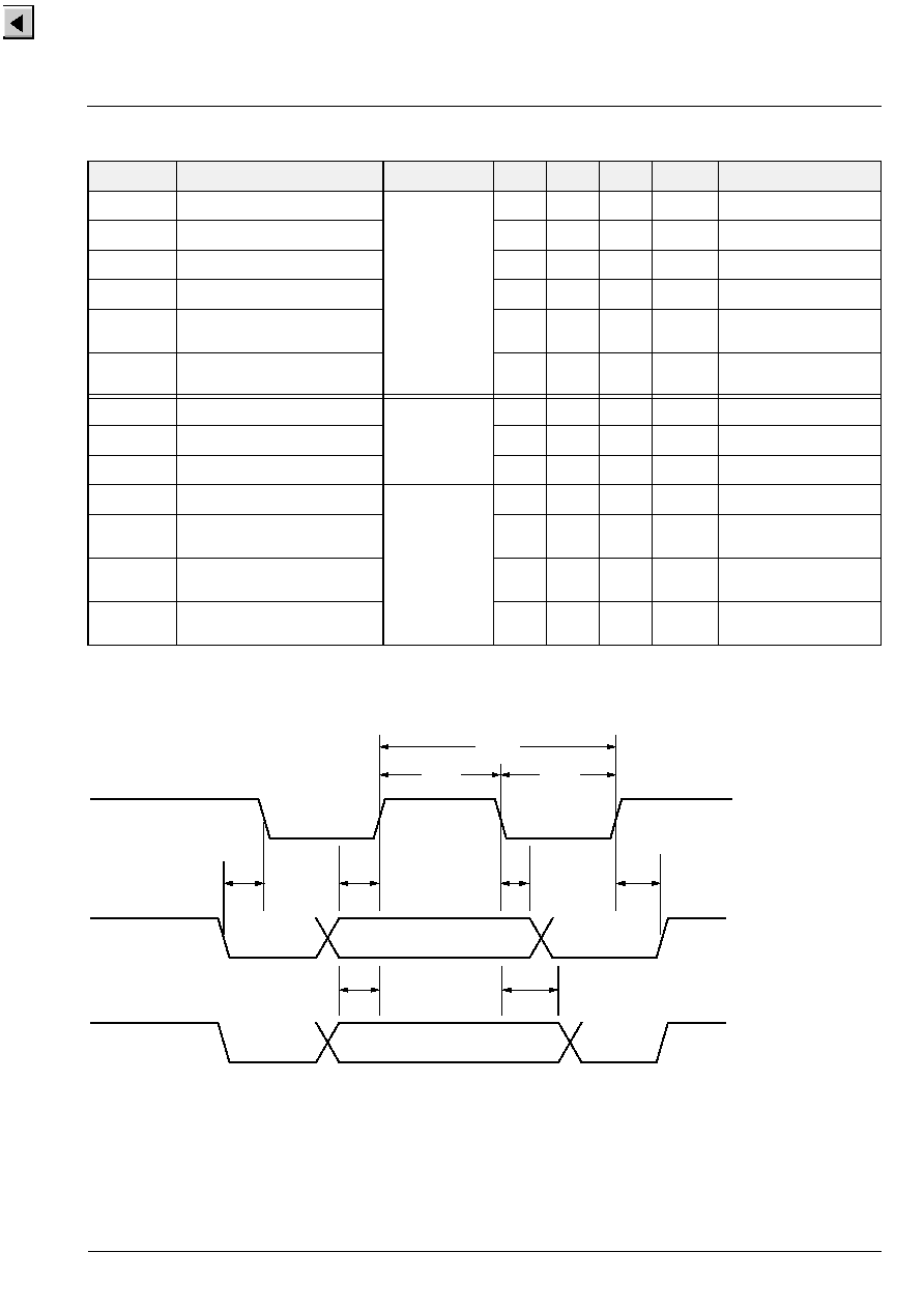
PRELIMINARY DATA SHEET
MSP 34x5G
Micronas
61
4.6.3.4. I
2
C Bus Characteristics
Fig. 4�27: I
2
C bus timing diagram
Symbol
Parameter
Pin Name
Min.
Typ.
Max.
Unit
Test Conditions
V
I2CIL
I
2
C-Bus Input Low Voltage
I2C_CL,
I2C_DA
0.3
V
SUP2
V
I2CIH
I
2
C-Bus Input High Voltage
0.6
V
SUP2
t
I2C1
I
2
C Start Condition Setup Time
120
ns
t
I2C2
I
2
C Stop Condition Setup Time
120
ns
t
I2C5
I
2
C-Data Setup Time
before Rising Edge of Clock
55
ns
t
I2C6
I
2
C-Data Hold Time
after Falling Edge of Clock
55
ns
t
I2C3
I
2
C-Clock Low Pulse Time
I2C_CL
500
ns
t
I2C4
I
2
C-Clock High Pulse Time
500
ns
f
I2C
I
2
C-BUS Frequency
1.0
MHz
V
I2COL
I
2
C-Data Output Low Voltage
I2C_CL,
I2C_DA
0.4
V
I
I2COL
= 3 mA
I
I2COH
I
2
C-Data Output
High Leakage Current
1.0
�
A
V
I2COH
= 5 V
t
I2COL1
I
2
C-Data Output Hold Time
after Falling Edge of Clock
15
ns
t
I2COL2
I
2
C-Data Output Setup Time
before Rising Edge of Clock
100
ns
f
I2C
= 1 MHz
I2C_CL
I2C_DA as input
I2C_DA as output
T
I2C1
T
I2C5
T
I2C6
T
I2C2
T
I2C4
T
I2C3
1/F
I2C
T
I2COL2
T
I2COL1
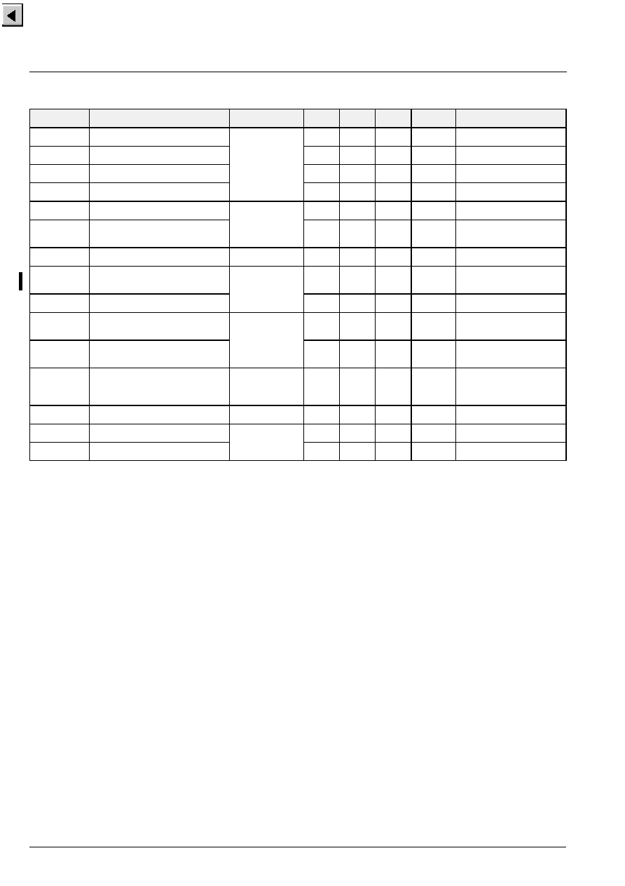
MSP 34x5G
PRELIMINARY DATA SHEET
62
Micronas
4.6.3.5. I
2
S-Bus Characteristics
Symbol
Parameter
Pin Name
Min.
Typ.
Max.
Unit
Test Conditions
V
I2SIL
Input Low Voltage
I2S_CL
I2S_WS
I2S_DA_IN1/2
0.2
V
SUP2
V
I2SIH
Input High Voltage
0.5
V
SUP2
Z
I2SI
Input Impedance
5
pF
I
LEAKI2S
Input Leakage Current
-
1
1
�
A
0 V < U
INPUT
< DVSUP
V
I2SOL
I
2
S Output Low Voltage
I2S_CL
I2S_WS
I2S_DA_OUT
0.4
V
I
I2SOL
= 1 mA
V
I2SOH
I
2
S Output High Voltage
V
SUP2
-
0.3
V
I
I2SOH
=
-
1 mA
f
I2SOWS
I
2
S-Word Strobe Output Frequency
I2S_WS
32.0
kHz
f
I2SOCL
I
2
S-Clock Output Frequency
I2S_CL
1.024
2.048
MHz
MHz
I2S_CONFIG[0] = 0
I2S_CONFIG[0] = 1
R
I2S10/I2S20
I
2
S-Clock Output High/Low-Ratio
0.9
1.0
1.1
t
s_I2S
I
2
S Input Setup Time
before Rising Edge of Clock
I2S_CL
I2S_DA_IN1/2
12
ns
for details see Fig. 4�28
"I
2
S timing diagram"
t
h_I2S
I
2
S Input Hold Time
after Rising Edge of Clock
40
ns
t
d_I2S
I
2
S Output Delay Time
after Falling Edge of Clock
I2S_CL
I2S_WS
I2S_DA_OUT
28
ns
C
L
= 30 pF
f
I2SWS
I
2
S-Word Strobe Input Frequency
I2S_WS
32.0
kHz
f
I2SCL
I
2
S-Clock Input Frequency
I2S_CL
1.024
MHz
R
I2SCL
I
2
S-Clock Input High/Low Ratio
0.9
1.1
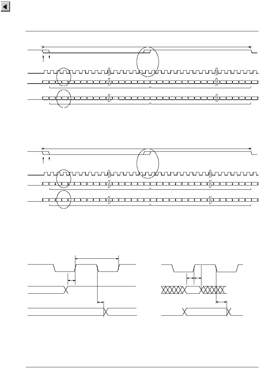
PRELIMINARY DATA SHEET
MSP 34x5G
Micronas
63
Fig. 4�28: I
2
S timing diagram
Data: MSB first, I
2
S master
R LSB L LSB
R LSB L LSB
16/32 bit right channel
L LSB
L LSB
R MSB
R MSB
Detail C
I2S_WS
I2S_CL
I2S_DA_IN
Detail A
MODUS[6] = 1
MODUS[6] = 0
Detail B
R LSB
R LSB L MSB
L MSB
I2S_DA_OUT
16/32 bit right channel
16/32 bit left channel
16/32 bit left channel
1/F
I2SWS
I2S_CL
Detail C
I2S_WS as INPUT
I2S_WS as OUTPUT
1/F
I2SCL
T
s_I2S
T
d_I2S
Detail A,B
I2S_CL
I2S_DA_OUT
T
d_I2S
Data: MSB first, I
2
S slave
R LSB L LSB
R LSB L LSB
16, 18...32 bit right channel
L LSB
L LSB
R MSB
R MSB
Detail C
I2S_WS
I2S_CL
I2S_DA_IN
Detail A
MODUS[6] = 1
MODUS[6] = 0
Detail B
R LSB
R LSB L MSB
L MSB
I2S_DA_OUT
16, 18...32 bit right channel
16, 18...32 bit left channel
16,18...32 bit left channel
1/F
I2SWS
T
h_I2S
T
s_I2S
I2S_DA_IN1/2
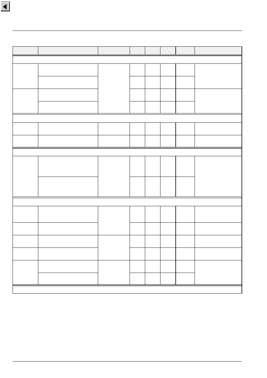
MSP 34x5G
PRELIMINARY DATA SHEET
64
Micronas
4.6.3.6. Analog Baseband Inputs and Outputs, AGNDC
Symbol
Parameter
Pin Name
Min.
Typ.
Max.
Unit
Test Conditions
Analog Ground
V
AGNDC0
AGNDC Open Circuit Voltage
(AHVSUP = 8 V)
AGNDC
3.77
V
R
load
10 M
AGNDC Open Circuit Voltage
(AHVSUP = 5 V)
2.51
V
R
outAGN
AGNDC Output Resistance
(AHVSUP = 8 V)
70
125
180
k
3 V
V
AGNDC
4 V
AGNDC Output Resistance
(AHVSUP = 5 V)
47
83
120
k
Analog Input Resistance
R
inSC
SCART Input Resistance
from T
A
= 0 to 70
�
C
SCn_IN_s
1)
25
40
58
k
f
signal
= 1 kHz, I = 0.05 mA
R
inMONO
MONO Input Resistance
from T
A
= 0 to 70
�
C
MONO_IN
15
24
35
k
f
signal
= 1 kHz, I = 0.1 mA
Audio Analog-to-Digital-Converter
V
AICL
Analog Input Clipping Level for
Analog-to-Digital-
Conversion
(AHVSUP = 8 V)
SCn_IN_s,
1)
MONO_IN
2.00
2.25
V
RMS
f
signal
= 1 kHz
Analog Input Clipping Level for
Analog-to-Digital-
Conversion
(AHVSUP = 5 V)
1.13
1.51
V
RMS
SCART Output
R
outSC
SCART Output Resistance
SCn_OUT_s
1)
200
200
330
460
500
f
signal
= 1 kHz, I = 0.1 mA
T
j
= 27
�
C
T
A
= 0 to 70
�
C
dV
OUTSC
Deviation of DC-Level at SCART
Output from AGNDC Voltage
-
70
+
70
mV
A
SCtoSC
Gain from Analog Input
to SCART Output
SCn_IN_s,
1)
MONO_IN
SCn_OUT_s
1)
-
1.0
+
0.5
dB
f
signal
= 1 kHz
f
rSCtoSC
Frequency Response from Analog
Input to SCART Output
-
0.5
+
0.5
dB
with resp. to 1 kHz
Bandwidth: 0 to 20000 Hz
V
outSC
Signal Level at SCART Output
(AHVSUP = 8 V)
SCn_OUT_s
1)
1.8
1.9
2.0
V
RMS
f
signal
= 1 kHz
Volume 0 dB
Full Scale input from I
2
S
Signal Level at SCART Output
(AHVSUP = 5V)
1.17
1.27
1.37
V
RMS
1)
"n" means "1"or "2"; "s" means "L" or "R"
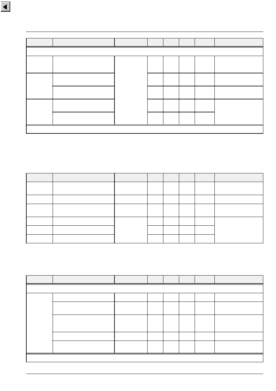
PRELIMINARY DATA SHEET
MSP 34x5G
Micronas
65
4.6.3.7. Sound IF Input
4.6.3.8. Power Supply Rejection
Main Output
R
outMA
Main Output Resistance
DACM_s
1)
2.1
2.1
3.3
4.6
5.0
k
k
f
signal
= 1 kHz, I = 0.1 mA
T
j
= 27
�
C
T
A
= 0 to 70
�
C
V
outDCMA
DC-Level at Main-Output
(AHVSUP = 8 V)
1.80
2.04
61
2.28
V
mV
Volume 0 dB
Volume
-
30 dB
DC-Level at Main-Output
(AHVSUP = 5 V)
1.12
1.36
40
1.60
V
mV
Volume 0 dB
Volume
-
30 dB
V
outMA
Signal Level at Main-Output
(AHVSUP = 8 V)
1.23
1.37
1.51
V
RMS
f
signal
= 1 kHz
Volume 0 dB
Full scale input from I
2
S
Signal Level at Main-Output
(AHVSUP = 5 V)
0.76
0.90
1.04
V
RMS
1)
"s" means "L" or "R"
Symbol
Parameter
Pin Name
Min.
Typ.
Max.
Unit
Test Conditions
R
IFIN
Input Impedance
ANA_IN1+,
ANA_IN
-
1.5
6.8
2
9.1
2.5
11.4
k
k
Gain AGC = 20 dB
Gain AGC = 3 dB
DC
VREFTOP
DC Voltage at VREFTOP
VREFTOP
2.4
2.65
2.75
V
DC
ANA_IN
DC Voltage on IF Inputs
ANA_IN1+,
ANA_IN
-
1.3
1.5
1.7
V
XTALK
IF
Crosstalk Attenuation
ANA_IN1+,
ANA_IN
-
40
dB
f
signal
= 1 MHz
Input Level =
-
2 dBr
BW
IF
3 dB Bandwidth
10
MHz
AGC
AGC Step Width
0.85
dB
Symbol
Parameter
Pin Name
Min.
Typ.
Max.
Unit
Test Conditions
PSRR: Rejection of Noise on AHVSUP at 1 kHz
PSRR
AGNDC
AGNDC
80
dB
From Analog Input to I
2
S Output
MONO_IN,
SCn_IN_s
1)
70
dB
From Analog Input to
SCART Output
MONO_IN,
SCn_IN_s
1)
SCn_OUT_s
1)
70
dB
From I
2
S Input to SCART Output
SCn_OUT_s
1)
60
dB
From I
2
S Input to MAIN or AUX
Output
DACM_s
1)
80
dB
1)
"n" means "1" or "2"; "s" means "L" or "R"
Symbol
Parameter
Pin Name
Min.
Typ.
Max.
Unit
Test Conditions
MSP 34x5G
PRELIMINARY DATA SHEET
66
Micronas
4.6.3.9. Analog Performance
Symbol
Parameter
Pin Name
Min.
Typ.
Max.
Unit
Test Conditions
Specifications for AHVSUP = 8 V
SNR
Signal-to-Noise Ratio
from Analog Input to I
2
S Output
MONO_IN,
SCn_IN_s
1)
85
88
dB
Input Level =
-
20 dB with
resp. to V
AICL
, f
sig
= 1 kHz,
unweighted
20 Hz...16 kHz
from Analog Input to
SCART Output
MONO_IN,
SCn_IN_s
1)
SCn_OUT_s
1)
93
96
dB
Input Level =
-
20 dB,
f
sig
= 1 kHz,
unweighted
20 Hz...20 kHz
from I
2
S Input to SCART Output
SCn_OUT_s
1)
85
88
dB
Input Level =
-
20 dB,
f
sig
= 1 kHz,
unweighted
20 Hz...16 kHz
from I
2
S Input to Main Output
for Analog Volume at 0 dB
for Analog Volume at
-
30 dB
DACM_s
1)
85
78
88
83
dB
dB
Input Level =
-
20 dB,
f
sig
= 1 kHz,
unweighted
20 Hz...16 kHz
THD
Total Harmonic Distortion
from Analog Input to I
2
S Output
MONO_IN,
SCn_IN_s
1)
0.01
0.03
%
Input Level =
-
3 dBr with
resp. to V
AICL
, f
sig
= 1 kHz,
unweighted
20 Hz...16 kHz
from Analog Input to
SCART Output
MONO_IN,
SCn_IN_s
SCn_OUT_s
1)
0.01
0.03
%
Input Level =
-
3 dBr,
f
sig
= 1 kHz,
unweighted
20 Hz...20 kHz
from I
2
S Input to SCART Output
SCn_OUT_s
1)
0.01
0.03
%
Input Level =
-
3 dBr,
f
sig
= 1 kHz,
unweighted
20 Hz...16 kHz
from I
2
S Input to Main Output
DACM_s
1)
0.01
0.03
%
Input Level =
-
3 dBr,
f
sig
= 1 kHz,
unweighted
20 Hz...16 kHz
1)
"n" means "1" or "2"; "s" means "L" or "R"
PRELIMINARY DATA SHEET
MSP 34x5G
Micronas
67
Specifications for AHVSUP = 5 V
SNR
Signal-to-Noise Ratio
from Analog Input to I
2
S Output
MONO_IN,
SCn_IN_s
1)
82
85
dB
Input Level =
-
20 dB with
resp. to V
AICL
, f
sig
= 1 kHz,
unweighted
20 Hz...16 kHz
from Analog Input to
SCART Output
MONO_IN,
SCn_IN_s
1)
SCn_OUT_s
1)
90
93
dB
Input Level =
-
20 dB,
f
sig
= 1 kHz,
unweighted
20 Hz...20 kHz
from I
2
S Input to SCART Output
SCn_OUT_s
1)
82
85
dB
Input Level =
-
20 dB,
f
sig
= 1 kHz,
unweighted
20 Hz...16 kHz
from I
2
S Input to Main Output
for Analog Volume at 0 dB
for Analog Volume at
-
30 dB
DACM_s
1)
82
75
85
80
dB
dB
Input Level =
-
20 dB,
f
sig
= 1 kHz,
unweighted
20 Hz...16 kHz
THD
Total Harmonic Distortion
from Analog Input to I
2
S Output
MONO_IN,
SCn_IN_s
1)
0.03
0.1
%
Input Level =
-
3 dBr with
resp. to V
AICL
, f
sig
= 1 kHz,
unweighted
20 Hz...16 kHz
from Analog Input to
SCART Output
MONO_IN,
SCn_IN_s
SCn_OUT_s
1)
0.1
%
Input Level =
-
3 dBr,
f
sig
= 1 kHz,
unweighted
20 Hz...20 kHz
from I
2
S Input to SCART Output
SCn_OUT_s
1)
0.1
%
Input Level =
-
3 dBr,
f
sig
= 1 kHz,
unweighted
20 Hz...16 kHz
from I
2
S Input to Main Output
DACM_s
1)
0.1
%
Input Level =
-
3 dBr,
f
sig
= 1 kHz,
unweighted
20 Hz...16 kHz
1)
"n" means "1" or "2"; "s" means "L" or "R"
Symbol
Parameter
Pin Name
Min.
Typ.
Max.
Unit
Test Conditions
MSP 34x5G
PRELIMINARY DATA SHEET
68
Micronas
CROSSTALK Specifications for AHVSUP = 8 V and 5 V
XTALK
Crosstalk Attenuation
Input Level =
-
3 dB,
f
sig
= 1 kHz, unused
analog inputs connected to
ground by Z < 1 k
between left and right channel within
SCART Input/Output pair (L
R, R
L)
SCn_IN
1)
SC1_OUT
SC1_IN or SC2_IN
I
2
S Output
SC3_IN
I
2
S Output
I
2
S Input
SC1_OUT
80
80
80
80
dB
dB
dB
dB
unweighted
20 Hz...20 kHz
between left and right channel within
Main or AUX Output pair
I
2
S Input
DACM
75
dB
unweighted
20 Hz...16 kHz
between SCART Input/Output pairs
D = disturbing program
O = observed program
D: MONO/SCn_IN
1)
SC1_OUT
O: MONO/SCn_IN
1)
SC1_OUT
D: MONO/SCn_IN
1)
SC1_OUT or unsel.
O: MONO/SCn_IN
1)
I
2
S Output
D: MONO/SCn_IN
1)
SC1_OUT
O: I
2
S Input
SC1_OUT
D: MONO/SCn_IN
1)
unselected
O: I
2
S Input
SC1_OUT
100
95
100
100
dB
dB
dB
dB
(unweighted
20 Hz...20 kHz
same signal source on left
and right disturbing
channel, effect on each
observed output channel
Crosstalk between Main and AUX Output pairs
I
2
S Input
DACM
90
dB
(unweighted
20 Hz...16 kHz)
same signal source on left
and right disturbing
channel, effect on each
observed output channel
XTALK
Crosstalk from Main or AUX Output to SCART Output
and vice versa
D = disturbing program
O = observed program
D: MONO/SCn_IN/DSP
1)
SC1_OUT
O: I
2
S Input
DACM
D: MONO/SCn_IN/DSP
1)
SC1_OUT
O: I
2
S Input
DACM
D: I
2
S Input
DACM
O: MONO/SCn_IN
1)
SC1_OUT
D: I
2
S Input
DACM
O: I
2
S Input
SC1_OUT
80
85
95
95
dB
dB
dB
dB
(unweighted
20 Hz...20 kHz)
same signal source on left
and right disturbing
channel, effect on each
observed output channel
SCART output load
resistance 10 k
SCART output load
resistance 30 k
1)
"n" means "1" or "2"; "s" means "L" or "R"
Symbol
Parameter
Pin Name
Min.
Typ.
Max.
Unit
Test Conditions
PRELIMINARY DATA SHEET
MSP 34x5G
Micronas
69
4.6.3.10. Sound Standard Dependent Characteristics
Symbol
Parameter
Pin Name
Min.
Typ.
Max.
Unit
Test Conditions
NICAM Characteristics (MSP Standard Code = 8)
dV
NICAMOUT
Tolerance of Output Voltage
of NICAM Baseband Signal
DACM_s,
SC1_OUT_s
1)
-
1.5
+
1.5
dB
2.12 kHz, Modulator input
level = 0 dBref
S/N
NICAM
S/N of NICAM Baseband Signal
72
dB
NICAM:
-
6 dB, 1 kHz, RMS
unweighted
0 to 15 kHz, Vol = 9 dB
NIC_Presc = 7F
hex
Output level 1 V
RMS
at
DACM_s
THD
NICAM
Total Harmonic Distortion
+
Noise
of NICAM Baseband Signal
0.1
%
2.12 kHz, Modulator input
level = 0 dBref
BER
NICAM
NICAM: Bit Error Rate
1
10
-
7
FM
+
NICAM, norm conditions
fR
NICAM
NICAM Frequency Response,
20...15000 Hz
-
1.0
+
1.0
dB
Modulator input
level =
-
12 dB dBref; RMS
XTALK
NICAM
NICAM Crosstalk Attenuation (Dual)
80
dB
SEP
NICAM
NICAM Channel Separation (Stereo)
80
dB
FM Characteristics (MSP Standard Code = 3)
dV
FMOUT
Tolerance of Output Voltage
of FM Demodulated Signal
DACM_s,
SC1_OUT_s
1)
-
1.5
+
1.5
dB
1 FM-carrier, 50
�
s, 1 kHz,
40 kHz deviation; RMS
S/N
FM
S/N of FM Demodulated Signal
73
dB
1 FM-carrier 5.5 MHz, 50
�
s,
1 kHz, 40 kHz deviation;
RMS, unweighted
0 to 15 kHz (for S/N);
full input range, FM-Pres-
cale = 46
hex
, Vol = 0 dB
Output Level 1 V
RMS
at
DACM_s
THD
FM
Total Harmonic Distortion
+
Noise
of FM Demodulated Signal
0.1
%
fR
FM
FM Frequency Responses,
20...15000 Hz
-
1.0
+
1.0
dB
1 FM-carrier 5.5 MHz,
50
�
s, Modulator input
level =
-
14.6 dBref; RMS
XTALK
FM
FM Crosstalk Attenuation (Dual)
80
dB
2 FM-carriers 5.5/5.74 MHz,
50
�
s, 1 kHz, 40 kHz
deviation; Bandpass 1 kHz
SEP
FM
FM Channel Separation (Stereo)
50
dB
2 FM-carriers 5.5/5.74 MHz,
50
�
s, 1 kHz, 40 kHz
deviation; RMS
AM Characteristics (MSP Standard Code = 9)
S/N
AM(1)
S/N of AM Demodulated Signal
measurement condition: RMS/Flat
DACM_s,
SC1_OUT_s
1)
55
dB
SIF level: 0.1
-
0.8 V
pp
AM-carrier 54% at 6.5 MHz
Vol = 0 dB, FM/AM
prescaler set for
output = 0.5 V
RMS
at
Loudspeaker out;
Standard Code = 09
hex
no video/chroma
components
S/N
AM(2)
S/N of AM Demodulated Signal
measurement condition: QP/CCIR
45
dB
THD
AM
Total Harmonic Distortion
+
Noise
of AM Demodulated Signal
0.6
%
fR
AM
AM Frequency Response
50...12000 Hz
-
2.5
+
1.0
dB
1) "s" means "L" or "R"

MSP 34x5G
PRELIMINARY DATA SHEET
70
Micronas
BTSC Characteristics (MSP Standard Code = 20
hex
, 21
hex
)
S/N
BTSC
S/N of BTSC Stereo Signal
S/N of BTSC-SAP Signal
DACM_s,
SC1_OUT_s
1)
68
57
dB
dB
1 kHz L or R or SAP, 100%
modulation, 75
�
s deempha-
sis, RMS unweighted 0 to 15
kHz
THD
BTSC
THD
+
N of BTSC Stereo Signal
THD
+
N of BTSC SAP Signal
0.1
0.5
%
%
1 kHz L or R or SAP, 100%
75
�
s EIM
2)
, DBX NR or
MNR, RMS unweighted
0 to 15 kHz
fR
DBX
Frequency Response of BTSC
Stereo, 50 Hz...12 kHz
Frequency Response of BTSC-
SAP, 50 Hz...9 kHz
-
1.0
-
1.0
1.0
1.0
dB
dB
L or R or SAP,
1%...66% EIM
2)
, DBX NR
fR
MNR
Frequency Response of BTSC
Stereo, 50 Hz...12 kHz
-
2.0
2.0
dB
L or R 5%...66% EIM
2)
, MNR
Frequency Response of BTSC-
SAP, 50 Hz...9 kHz
-
2.0
2.0
dB
SAP, white noise, 10% Modu-
lation, MNR
XTALK
BTSC
Stereo
SAP
SAP
Stereo
76
80
dB
dB
1 kHz L or R or SAP, 100%
modulation, 75
�
s deempha-
sis, Bandpass 1 kHz
SEP
DBX
Stereo Separation DBX NR
50 Hz...10 kHz
50 Hz...12 kHz
35
30
dB
dB
L or R 1%...66% EIM
2)
, DBX
NR
SEP
MNR
Stereo Separation MNR
30
dB
L = 300 Hz, R = 3.1 kHz
14% Modulation, MNR
FM
pil
Pilot deviation threshold
Stereo off
on
Stereo on
off
ANA_IN1+
3.2
1.2
3.5
1.5
kHz
kHz
4.5 MHz carrier modulated
with f
h
= 15.734 kHz
SIF level = 100 mV
pp
indication: STATUS Bit[6]
f
Pilot
Pilot Frequency Range
15.563
15.843
kHz
standard BTSC stereo signal,
sound carrier only
1)
"s" means "L" or "R"
2)
EIM refers to 75-
�
s Equivalent Input Modulation. It is defined as the audio-signal level which results in a stated percentage modulation,
when the DBX encoding process is replaced by a 75-
�
s preemphasis network.
Symbol
Parameter
Pin Name
Min.
Typ.
Max.
Unit
Test Conditions
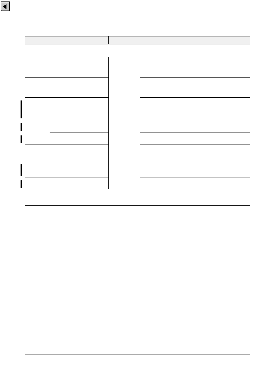
PRELIMINARY DATA SHEET
MSP 34x5G
Micronas
71
BTSC Characteristics (MSP Standard Code = 20
hex
, 21
hex
)
with a minimum IF input signal level of 70 mVpp (measured without any video/chroma signal components)
S/N
BTSC
S/N of BTSC Stereo Signal
S/N of BTSC-SAP Signal
DACM_s,
SC1_OUT_s
1)
64
55
dB
dB
1 kHz L or R or SAP, 100%
modulation, 75
�
s deempha-
sis, RMS unweighted 0 to 15
kHz
THD
BTSC
THD
+
N of BTSC Stereo Signal
THD
+
N of BTSC SAP Signal
0.15
0.8
%
%
1 kHz L or R or SAP, 100%
75
�
s EIM
2)
, DBX NR or
MNR, RMS unweighted
0 to 15 kHz
fR
DBX
Frequency Response of BTSC
Stereo, 50 Hz...12 kHz
Frequency Response of BTSC-
SAP, 50 Hz...9 kHz
-
1.0
-
1.0
1.0
1.0
dB
dB
L or R or SAP,
1%...66% EIM
2)
, DBX NR
fR
MNR
Frequency Response of BTSC
Stereo, 50 Hz...12 kHz
-
2.0
2.0
dB
L or R 5%...66% EIM
2)
, MNR
Frequency Response of BTSC-
SAP, 50 Hz...9 kHz
-
2.0
2.0
dB
SAP, white noise, 10% Modu-
lation, MNR
XTALK
BTSC
Stereo
SAP
SAP
Stereo
75
75
dB
dB
1 kHz L or R or SAP, 100%
modulation, 75
�
s deempha-
sis, Bandpass 1 kHz
SEP
DBX
Stereo Separation DBX NR
50 Hz...10 kHz
50 Hz...12 kHz
35
30
dB
dB
L or R 1%...66% EIM
2)
, DBX
NR
SEP
MNR
Stereo Separation MNR
30
dB
L = 300 Hz, R = 3.1 kHz
14% Modulation, MNR
1)
"s" means "L" or "R"
2)
EIM refers to 75-
�
s Equivalent Input Modulation. It is defined as the audio-signal level which results in a stated percentage modulation,
when the DBX encoding process is replaced by a 75-
�
s preemphasis network.
Symbol
Parameter
Pin Name
Min.
Typ.
Max.
Unit
Test Conditions

MSP 34x5G
PRELIMINARY DATA SHEET
72
Micronas
EIA-J Characteristics (MSP Standard Code = 30
hex
)
S/N
EIAJ
S/N of EIA-J Stereo Signal
S/N of EIA-J Sub-Channel
DACM_s,
SC1_OUT_s
1)
60
60
dB
dB
1 kHz L or R,
100% modulation,
75
�
s deemphasis,
RMS unweighted
0 to 15 kHz
THD
EIAJ
THD
+
N of EIA-J Stereo Signal
THD
+
N of EIA-J Sub-Channel
0.2
0.3
%
%
fR
EIAJ
Frequency Response of EIA-J
Stereo, 50 Hz...12 kHz
Frequency Response of EIA-J
Sub-Channel, 50 Hz...12 kHz
-
1.0
-
1.0
1.0
1.0
dB
dB
100% modulation,
75
�
s deemphasis
XTALK
EIAJ
Main
SUB
Sub
MAIN
66
80
dB
dB
1 kHz L or R, 100%
modulation, 75
�
s
deemphasis,
Bandpass 1 kHz
SEP
EIAJ
Stereo Separation
50 Hz...5 kHz
50 Hz...10 kHz
35
28
dB
dB
EIA-J Stereo Signal, L or R
100% modulation
FM-Radio Characteristics (MSP Standard Code = 40
hex
)
S/N
UKW
S/N of FM-Radio Stereo Signal
DACM_s,
SC1_OUT_s
1)
68
dB
1 kHz L or R, 100%
modulation, 75
�
s
deemphasis, RMS
unweighted
0 to 15 kHz
THD
UKW
THD
+
N of FM-Radio Stereo Signal
0.1
%
fR
UKW
Frequency Response of
FM-Radio Stereo
50 Hz...15 kHz
-
1.0
+
1.0
dB
L or R, 1%...100%
modulation, 75
�
s
deemphasis
SEP
UKW
Stereo Separation 50 Hz...15 kHz
45
dB
f
Pilot
Pilot Frequency Range
ANA_IN1+
18.844
19.125
kHz
standard FM radio
stereo signal
1)
"s" means "L" or "R"
Symbol
Parameter
Pin Name
Min.
Typ.
Max.
Unit
Test Conditions

PRELIMINARY DATA SHEET
MSP 34x5G
Micronas
73
5. Appendix A: Overview of TV Sound Standards
5.1. NICAM 728
Table 5�1: Summary of NICAM 728 sound modulation parameters
Specification
I
B/G
L
D/K
Carrier frequency of
digital sound
6.552 MHz
5.85 MHz
5.85 MHz
5.85 MHz
Transmission rate
728 kbit/s
Type of modulation
Differentially encoded quadrature phase shift keying (DQPSK)
Spectrum shaping
Roll-off factor
by means of Roll-off filters
1.0
0.4
0.4
0.4
Carrier frequency of
analog sound component
6.0 MHz
FM mono
5.5 MHz
FM mono
6.5 MHz AM mono
6.5 MHz
FM mono
terrestrial
cable
Power ratio between
vision carrier and
analog sound carrier
10 dB
13 dB
10 dB
16 dB
13 dB
Power ratio between
analog and modulated
digital sound carrier
10 dB
7 dB
17 dB
11 dB
China/
Hungary
Poland
12 dB
7 dB
Table 5�2: Summary of NICAM 728 sound coding characteristics
Characteristics
Values
Audio sampling frequency
32 kHz
Number of channels
2
Initial resolution
14 bit/sample
Companding characteristics
near instantaneous, with compression to 10 bits/sample in 32-samples (1 ms) blocks
Coding for compressed samples
2's complement
Preemphasis
CCITT Recommendation J.17 (6.5 dB attenuation at 800 Hz)
Audio overload level
+12 dBm measured at the unity gain frequency of the preemphasis network (2 kHz)
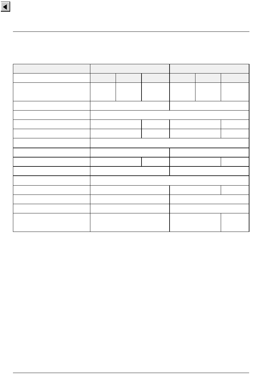
MSP 34x5G
PRELIMINARY DATA SHEET
74
Micronas
5.2. A2 Systems
Table 5�3: Key parameters for A2 Systems of Standards B/G, D/K, and M
Characteristics
Sound Carrier FM1
Sound Carrier FM2
TV-Sound Standard
B/G
D/K
M
B/G
D/K
M
Carrier frequency in MHz
5.5
6.5
4.5
5.7421875
6.2578125
6.7421875
5.7421875
4.724212
Vision/sound power difference
13 dB
20 dB
Sound bandwidth
40 Hz to 15 kHz
Preemphasis
50
�
s
75
�
s
50
�
s
75
�
s
Frequency deviation (nom/max)
�
27
/�
50 kHz
�
17
/�
25 kHz
�
27
/�
50 kHz
�
15
/�
25 kHz
Transmission Modes
Mono transmission
mono
mono
Stereo transmission
(L
+
R)/2
(L
+
R)/2
R
(L
-
R)/2
Dual sound transmission
language A
language B
Identification of Transmission Mode
Pilot carrier frequency
54.6875 kHz
55.0699 kHz
Max. deviation portion
�
2.5 kHz
Type of modulation / modulation depth
AM / 50%
Modulation frequency
mono: unmodulated
stereo: 117.5 Hz
dual:
274.1 Hz
149.9 Hz
276.0 Hz
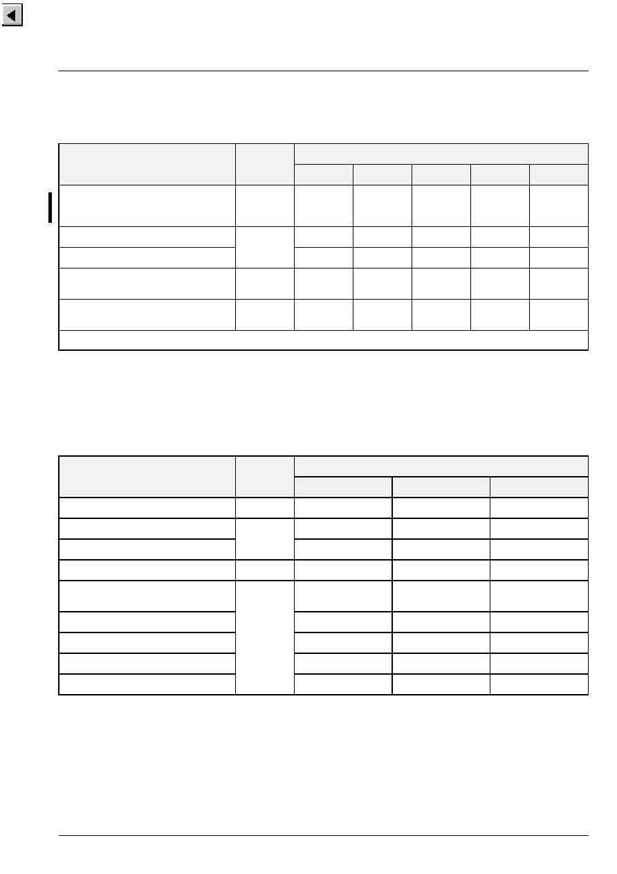
PRELIMINARY DATA SHEET
MSP 34x5G
Micronas
75
5.3. BTSC-Sound System
5.4. Japanese FM Stereo System (EIA-J)
Table 5�4: Key parameters for BTSC-Sound Systems
Aural
Carrier
BTSC-MPX-Components
(L
+
R)
Pilot
(L
-
R)
SAP
Prof. Ch.
Carrier frequency
(f
hNTSC
= 15.734 kHz)
(f
hPAL
= 15.625 kHz)
4.5 MHz
Baseband
f
h
2 f
h
5 f
h
6.5 f
h
Sound bandwidth in kHz
0.05 - 15
0.05 - 15
0.05 - 12
0.05 - 3.4
Preemphasis
75
�
s
DBX
DBX
150
�
s
Max. deviation to Aural Carrier
73 kHz
(total)
25 kHz
1)
5 kHz
50 kHz
1)
15 kHz
3 kHz
Max. Freq. Deviation of Subcarrier
Modulation Type
AM
10 kHz
FM
3 kHz
FM
1)
Sum does not exceed 50 kHz due to interleaving effects
Table 5�5: Key parameters for Japanese FM-Stereo Sound System EIA-J
Aural
Carrier
FM
EIA-J-MPX-Components
(L
+
R)
(L
-
R)
Identification
Carrier frequency (f
h
= 15.734 kHz)
4.5 MHz
Baseband
2 f
h
3.5 f
h
Sound bandwidth
0.05 - 15 kHz
0.05 - 15 kHz
-
Preemphasis
75
�
s
75
�
s
none
Max. deviation portion to Aural Carrier
47 kHz
25 kHz
20 kHz
2 kHz
Max. Freq. Deviation of Subcarrier
Modulation Type
10 kHz
FM
60%
AM
Transmitter-sided delay
20
�
s
0
�
s
0
�
s
Mono transmission
L
+
R
-
unmodulated
Stereo transmission
L
+
R
L
-
R
982.5 Hz
Bilingual transmission
Language A
Language B
922.5 Hz
MSP 34x5G
PRELIMINARY DATA SHEET
76
Micronas
5.5. FM Satellite Sound
5.6. FM-Stereo Radio
Table 5�6: Key parameters for FM Satellite Sound
Carrier Frequency
Maximum
FM Deviation
Sound Mode
Bandwidth
Deemphasis
6.5 MHz
85 kHz
Mono
15 kHz
50
�
s
7.02/7.20 MHz
50 kHz
Mono/Stereo/Bilingual
15 kHz
adaptive
7.38/7.56 MHz
50 kHz
Mono/Stereo/Bilingual
15 kHz
adaptive
7.74/7.92 MHz
50 kHz
Mono/Stereo/Bilingual
15 kHz
adaptive
Table 5�7: Key parameters for FM-Stereo Radio Systems
Aural
Carrier
FM-Radio-MPX-Components
(L
+
R)
Pilot
(L
-
R)
RDS/ARI
Carrier frequency (f
p
= 19 kHz)
10.7 MHz
Baseband
f
p
2 f
p
3 f
h
Sound bandwidth in kHz
0.05 - 15
0.05 - 15
Preemphasis:
-
USA
-
Europe
75
�
s
50
�
s
75
�
s
50
�
s
Max. deviation to Aural Carrier
75 kHz
(100%)
90%
1)
10%
90%
1)
5%
1)
Sum does not exceed 90% due to interleaving effects.

PRELIMINARY DATA SHEET
MSP 34x5G
Micronas
77
6. Appendix B: Manual/Compatibility Mode
To adapt the modes of the STANDARD SELECT regis-
ter to individual requirements and for reasons of com-
patibility to the MSP 34x5D, the MSP 34x5G offers
an Manual/Compatibility Mode, which provides sophis-
ticated programming of the MSP 34x5G.
Using the STANDARD SELECT register generally pro-
vides a more economic way to program the
MSP 34x5G and will result in optimal behavior. There-
fore, it is not recommend to use the Manual/Com-
patibility mode. In those cases, where the
MSP 34x5D is to be substituted by the MSP 34x5G,
the tips given in Section 6.9. on page 91 have to be
obeyed by the controller software.
6.1. Demodulator Write and Read Registers for Manual/Compatibility Mode
Table 6�1: Demodulator Write Registers; Subaddress: 10
hex
; these registers are not readable!
Demodulator
Write Registers
Address
(hex)
MSP-
Version
Description
Reset
Mode
Page
AUTO_FM/AM
00 21
3415,
3455
1. MODUS[0]=1 (Automatic Sound Select): Switching Level threshold of
Automatic Switching between NICAM and FM/AM in case of bad NICAM
reception
2. MODUS[0]=0 (Manual Mode): Activation and configuration of Automatic
Switching between NICAM and FM/AM in case of bad NICAM reception
00 00
79
A2_Threshold
00 22
all
A2 Stereo Identification Threshold
00 19
hex
81
CM_Threshold
00 24
all
Carrier-Mute Threshold
00 2A
hex
81
AD_CV
00 BB
all
SIF-input selection, configuration of AGC, and Carrier-Mute Function
00 00
82
MODE_REG
00 83
3415,
3455
Controlling of MSP-Demodulator and Interface options. As soon as this
register is applied, the MSP 34x5G works in the MSP 34x5D compatibility
mode.
Warning: In this mode, BTSC, EIA-J, and FM-Radio are disabled. Only
MSP 34x5D features are available; the use of MODUS and STATUS register
is not allowed.
The MSP 34x5G
is reset to the normal mode by first programming the
MODUS register followed by transmitting a valid standard code to the
STANDARD SELECTION register.
00 00
83
FIR1
FIR2
00 01
00 05
FIR1-filter coefficients channel 1 (6
8 bit)
FIR2-filter coefficients channel 2 (6
8 bit),
+
3
8 bit offset (total 72 bit)
00 00
85
DCO1_LO
DCO1_HI
DCO2_LO
DCO2_HI
00 93
00 9B
00 A3
00 AB
Increment channel 1 Low Part
Increment channel 1 High Part
Increment channel 2 Low Part
Increment channel 2 High Part
00 00
85
Note: All registers except AUTO_FM/AM, A2_Threshold, and CM_Threshold are initialized during STANDARD SELECTION and are
automatically updated when Automatic Sound Select (MODUS[0]=1) is on.

MSP 34x5G
PRELIMINARY DATA SHEET
78
Micronas
6.2. DSP Write and Read Registers for Manual/Compatibility Mode
Table 6�2: Demodulator Read Registers; Subaddress: 11
hex
; these registers are not writable!
Demodulator
Read Registers
Address
(hex)
MSP-
Version
Description
Page
C_AD_BITS
00 23
3415,
3455
NICAM-Sync bit, NICAM-C-Bits, and three LSBs of additional data bits
87
ADD_BITS
00 38
NICAM: bit [10:3] of additional data bits
87
CIB_BITS
00 3E
NICAM: CIB1 and CIB2 control bits
87
ERROR_RATE
00 57
NICAM error rate, updated with 182 ms
88
PLL_CAPS
02 1F
Not for customer use.
88
AGC_GAIN
02 1E
Not for customer use.
88
Table 6�3: DSP-Write Registers; Subaddress: 12
hex
, all registers are readable as well
Write Register
Address
(hex)
Bits
Operational Modes and Adjustable Range
Reset
Mode
Page
Volume SCART1 channel: Ctrl. mode
00 07
[7:0]
[Linear mode / logarithmic mode]
00
hex
89
FM Fixed Deemphasis
00 0F
[15:8]
[50
�
s, 75
�
s, J17, OFF]
50
�
s
89
FM Adaptive Deemphasis
[7:0]
[OFF, WP1]
OFF
89
Identification Mode
00 15
[7:0]
[B/G, M]
B/G
90
FM DC Notch
00 17
[7:0]
[ON, OFF]
ON
90
Table 6�4: DSP Read Registers; Subaddress: 13
hex
, all registers are not writable
Additional Read
Registers
Address
(hex)
Bits
Output Range
Page
Stereo detection register for
A2 Stereo Systems
00 18
[15:8]
[80
hex
... 7F
hex
]
8 bit two's complement
90
DC level readout FM1/Ch2-L
00 1B
[15:0]
[8000
hex
... 7FFF
hex
]
16 bit two's complement
90
DC level readout FM2/Ch1-R
00 1C
[15:0]
[8000
hex
... 7FFF
hex
]
16 bit two's complement
90
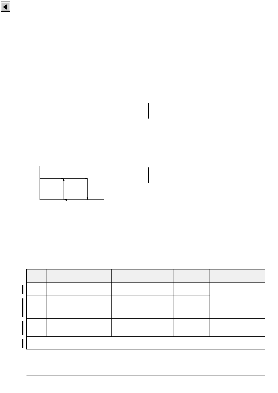
PRELIMINARY DATA SHEET
MSP 34x5G
Micronas
79
6.3. Manual/Compatibility Mode:
Description of Demodulator Write Registers
6.3.1. Automatic Switching between NICAM and
Analog Sound
In case of bad NICAM reception or loss of the
NICAM-carrier, the MSP 34x5G offers an Automatic
Switching (fall back) to the analog sound (FM/AM-
mono), without the necessity for the controller of reading
and evaluating any parameters. If a proper NICAM sig-
nal returns, switching back to this source is performed
automatically as well. The feature evaluates the NICAM
ERROR_RATE and switches, if necessary, all output
channels which are assigned to the NICAM-source, to
the analog source, and vice versa.
An appropriate hysteresis algorithm avoids oscillating
effects (see Fig. 6�1). STATUS[9] and C_AD_BITS[11]
(Addr: 0023 hex) provide information about the actual
NICAM-FM/AM-status.
Fig. 6�1: Hysteresis for Automatic Switching
6.3.1.1. Function in Automatic Sound Select Mode
The Automatic Sound Select feature (MODUS[0]=1)
includes the procedure mentioned above. By default, the
internal ERROR_RATE threshold is set to 700
dec
. i.e.:
� NICAM
analog Sound if ERROR_RATE
>
700
� analog Sound
NICAM if ERROR_RATE
<
700/2
The ERROR_RATE value of 700 corresponds to a
BER of approximately 5.46*10
-3
/s.
Individual configuration of the threshold can be done
using Table 6�5. However, the internal setting used by
the standard selection is recommended.
The optimum NICAM sound can be assigned to the
MSP output channels by selecting one of the "Stereo
or A/B", "Stereo or A", or "Stereo or B" source chan-
nels
6.3.1.2. Function in Manual Mode
If the manual mode (MODUS[0]=0) is required, the
activation and configuration of the Automatic Switching
feature has to be done as described in Table 6�6.
Note, that the channel matrix of the corresponding out-
put-channels must be set according to the
NICAM-mode and need not to be changed in the FM/
AM-fallback case.
Example:
Required threshold = 500: bits[10:1] = 00 1111 1010
ERROR_RATE
Selected Sound
NICAM
analog
sound
threshold
threshold/2
Table 6�5: Coding of Automatic NICAM/Analog Sound Switching;
Automatic Sound Select is on (MODUS[0] = 1)
Mode
Description
AUTO_FM [11:0]
Addr. = 00 21
hex
ERROR_RATE-
Threshold/dec
Source Select:
Input at NICAM Path
1)
1
Default
Automatic Switching with
internal threshold
bit[11:0] = 0
700
NICAM or FM/AM,
depending on
ERROR_RATE
2
Automatic Switching with
external threshold
(Customizing of Automatic
Sound Select)
bit[11]
= 0
bit[10:1] = 25...1000
= threshold/2
bit[0]
= 1
set by customer;
recommended
range: 50...2000
3
Forced Analog Mono
bit[11]
= 1
bit[10:1] = ignored
bit[0]
= 1
always FM/AM
1)
The NICAM path may be assigned to "Stereo or A/B", "Stereo or A", or "Stereo or B" source channels
(see Table 2�1 on page 11).
MSP 34x5G
PRELIMINARY DATA SHEET
80
Micronas
Table 6�6: Coding of Automatic NICAM/Analog Sound Switching;
Automatic Sound Select is off (MODUS[0] = 0)
Mode
Description
AUTO_FM [11:0]
Addr. = 00 21
hex
ERROR_RATE-
Threshold/dec
Source Select:
Input at NICAM Path
0
reset
status
Forced NICAM
(Automatic Switching disabled)
bit[11]
= 0
bit[10:1] = 0
bit[0]
= 0
none
always NICAM; Mute in
case of no NICAM available
1
Automatic Switching with
internal threshold
(Default, if Automatic Sound
Select is on)
bit[11]
= 0
bit[10:1] = 0
bit[0]
= 1
700
NICAM or FM/AM,
depending on
ERROR_RATE
2
Automatic Switching with
external threshold
(Customizing of Automatic
Sound Select)
bit[11]
= 0
bit[10:1] = 25...1000
= threshold/2
bit[0]
= 1
set by customer;
recommended
range: 50...2000
3
Forced Analog Mono
(Automatic Switching disabled)
bit[11]
= 1
bit[10:1] = 0
bit[0]
= 1
none
always FM/AM
PRELIMINARY DATA SHEET
MSP 34x5G
Micronas
81
6.3.2. A2 Threshold
The threshold between Stereo/Bilingual and Mono
Identification for the A2 Standard has been made pro-
grammable according to the user's preferences. An
internal hysteresis ensures robustness and stability.
6.3.3. Carrier-Mute Threshold
The Carrier-Mute threshold has been made program-
mable according to the user's preferences. An internal
hysteresis ensures stable behavior.
Table 6�7: Write Register on I
2
C Subaddress 10
hex
: A2 Threshold
Register
Address
Function
Name
THRESHOLDS
00 22
hex
(write)
A2 THRESHOLD Register
Defines threshold of all A2 and EIA_J standards for Stereo and Bilingual
detection
bit[15:0]
07F0
hex
force Mono Identification
...
0190
hex
default setting after reset
...
00A0
hex
minimum Threshold for stable detection
recommended range : 00A0
hex
...03C0
hex
A2_THRESH
Table 6�8: Write Register on I
2
C Subaddress 10
hex
: Carrier-Mute Threshold
Register
Address
Function
Name
THRESHOLDS
00 24
hex
(write)
Carrier-Mute THRESHOLD Register
Defines threshold for the carrier mute feature
bit[15:0]
0000
hex
Carrier-Mute always ON (both channels muted)
...
002A
hex
default setting after reset
...
07FF
hex
Carrier-Mute always OFF
(both channels forced on)
recommended range : 0014
hex
...0050
hex
CM_THRESH
MSP 34x5G
PRELIMINARY DATA SHEET
82
Micronas
6.3.4. Register AD_CV
The use of this register is no longer recommended.
Use it only in cases where compatibility to the
MSP 34x5D is required. Using the STANDARD
SELECTION register together with the MODUS regis-
ter provides a more economic way to program the
MSP 34x5G
Note: This register is initialized during STANDARD SELECTION and is automatically updated when Automatic
Sound Select (MODUS[0]=1) is on.
Table 6�9: AD_CV Register; reset status: all bits are "0"
AD_CV
(00 BB
hex
)
Automatic setting by
STANDARD SELECT Register
Bit
Function
Settings
2-8, 0A-51
hex
9
[0]
not used
must be set to 0
0
0
[1
:
6]
Reference level in case of Automatic Gain
Control = on (see Table 6�10). Constant gain
factor when Automatic Gain Control = off
(see Table 6�11).
101000
100011
[7]
Determination of Automatic Gain or
Constant Gain
0 = constant gain
1 = automatic gain
1
1
[8]
Selection of Sound IF source
(identical to MODUS[8])
0 = ANA_IN1+
X
X
[9]
MSP-Carrier-Mute Feature
0 = off: no mute
1 = on: mute as de-
scribed in Section 2.2.2.
1
1
[10
:
15]
not used
must be set to 0
0
0
X: not affected while choosing the TV sound standard by means of the STANDARD SELECT Register
Table 6�10: Reference values for active AGC (AD_CV[7] = 1)
Application
Input Signal Contains
AD_CV [6:1]
Ref. Value
AD_CV [6:1]
in decimal
Range of Input Signal
at pin ANA_IN1+
Terrestrial TV
-
Dual Carrier FM
-
NICAM/FM
-
NICAM/AM
-
NICAM only
2 FM Carriers
1 FM and 1 NICAM Carrier
1 AM and 1 NICAM Carrier
1 NICAM Carrier only
101000
101000
100011
010100
40
40
35
20
0.10
-
3 V
pp
1)
0.10
-
3 V
pp
1)
0.10
-
1.4 V
pp
(recommended: 0.10
-
0.8 V
pp
)
0.05
-
1.0 V
pp
SAT
1 or more FM Carriers
100011
35
0.10
-
3 V
pp
1)
ADR
FM and ADR carriers
see DRP 3510A data sheet
1)
For signals above 1.4 Vpp, the minimum gain of 3 dB is switched, and overflow of the A/D converter may result. Due to the
robustness of the internal processing, the IC works up to and even more than 3 Vpp, if norm conditions of FM/NICAM or
FM1/FM2 ratio are supposed. In this overflow case, a loss of FM-S/N-ratio of about 10 dB may appear.

PRELIMINARY DATA SHEET
MSP 34x5G
Micronas
83
6.3.5. Register MODE_REG
Note: The use of this register is no longer recom-
mended. It should be used only in cases where soft-
ware compatibility to the MSP 34x5D is required.
Using the STANDARD SELECTION register together
with the MODUS register provides a more economic
way to program the MSP 34x5G.
As soon as this register is applied, the MSP 34x5G
works in the MSP 34x5D Manual/Compatibility
Mode. In this mode, BTSC, EIA-J, and FM-Radio are
disabled. Only MSP 34x5D features are available; the
use of MODUS and STATUS register is not allowed.
The MSP 34x5G is reset to the normal mode by first
programming the MODUS register, followed by trans-
mitting a valid standard code to the STANDARD
SELECTION register.
The register `MODE_REG' contains the control bits
determining the operation mode of the MSP 34x5G in
the MSP 34x5D Manual/Compatibility Mode; Table 6�
12
explains all bit positions.
Table 6�11: AD_CV parameters for constant input gain (AD_CV[7]=0)
Step
AD_CV [6:1]
Constant Gain
Gain
Input Level at pin ANA_IN1+ and ANA_IN2+
0
1
2
3
4
5
6
7
8
9
10
11
12
13
14
15
16
17
18
19
20
000000
000001
000010
000011
000100
000101
000110
000111
001000
001001
001010
001011
001100
001101
001110
001111
010000
010001
010010
010011
010100
3.00 dB
3.85 dB
4.70 dB
5.55 dB
6.40 dB
7.25 dB
8.10 dB
8.95 dB
9.80 dB
10.65 dB
11.50 dB
12.35 dB
13.20 dB
14.05 dB
14.90 dB
15.75 dB
16.60 dB
17.45 dB
18.30 dB
19.15 dB
20.00 dB
maximum input level: 3 V
pp
(FM) or 1 V
pp
(NICAM)
1)
maximum input level: 0.14 V
pp
1)
For signals above 1.4 Vpp, the minimum gain of 3 dB is switched, and overflow of the A/D converter may result. Due to the
robustness of the internal processing, the IC works up to and even more than 3 Vpp, if norm conditions of FM/NICAM or
FM1/FM2 ratio are supposed. In this overflow case, a loss of FM-S/N-ratio of about 10 dB may appear.

MSP 34x5G
PRELIMINARY DATA SHEET
84
Micronas
Table 6�12: Control word `MODE_REG'; reset status: all bits are "0"
MODE_REG 00 83
hex
Automatic setting by
STANDARD SELECT Register
Bit
Function
Comment
Definition
2 - 5
8,A,B
9
[0]
not used
0 : must be used
0
0
0
[1]
DCTR_TRI
Digital control out
0/1 tri-state
0 : active
1 : tri-state
X
X
X
[2]
I
2
S_TRI
I
2
S outputs tri-state
(I2S_CL, I2S_WS,
I2S_DA_OUT)
0 : active
1 : tri-state
X
X
X
[3]
I
2
S Mode
1)
Master/Slave mode
of the I
2
S bus
0 : Master
1 : Slave
X
X
X
[4]
I
2
S_WS Mode
WS due to the Sony or
Philips-Format
0 : Sony
1 : Philips
X
X
X
[5]
not used
1 : recommended
X
X
X
[6]
NICAM
1)
Mode of MSP-Ch1
0 : FM
1 : Nicam
0
1
1
[7]
not used
0 : must be used
0
0
0
[8]
FM AM
Mode of MSP-Ch2
0 : FM
1 : AM
0
0
1
[9]
HDEV
High Deviation Mode
(channel matrix must be
sound A)
0 : normal
1 : high deviation mode
0
0
0
[11:10]
not used
0 : must be used
0
0
0
[12]
MSP-Ch1 Gain
see also Table 6�14
0 : Gain = 6 dB
1 : Gain = 0 dB
0
0
0
[13]
FIR1-Filter
Coeff. Set
see also Table 6�14
0 : use FIR1
1 : use FIR2
1
0
0
[14]
ADR
Mode of MSP-Ch1/
ADR-Interface
0 : normal mode/tri-state
1 : ADR-mode/active
0
0
0
[15]
AM-Gain
Gain for AM
Demodulation
0 : 0 dB (default. of MSPB)
1 : 12 dB (recommended)
1
1
1
1)
NICAM and I
2
S-Master mode are not allowed simultaneously
X: not affected by
STANDARD SELECT register
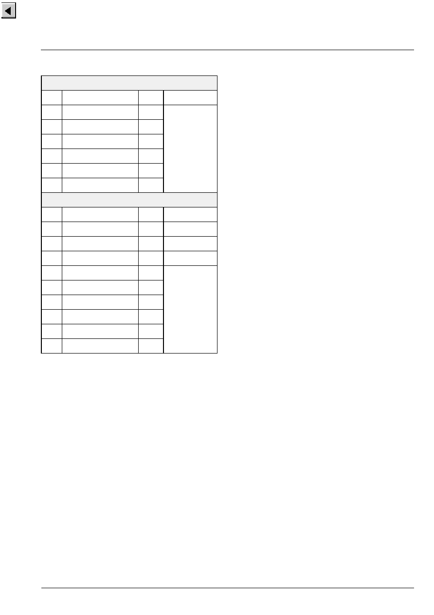
PRELIMINARY DATA SHEET
MSP 34x5G
Micronas
85
6.3.6. FIR-Parameter, Registers FIR1 and FIR2
Note: The use of this register is no longer recom-
mended. Use it only in cases where software compati-
bility to the MSP 34x5D is required. Using the STAN-
DARD SELECTION register together with the MODUS
register provides a more economic way to program the
MSP 34x5G.
Data shaping and/or FM/AM bandwidth limitation is
performed by a pair of linear phase Finite Impulse
Response filters (FIR-filter). The filter coefficients are
programmable and either are configured automatically
by the STANDARD SELECT register or written manu-
ally by the control processor via the control bus. Two
not necessarily different sets of coefficients are
required: one for MSP-Ch1 (NICAM or FM2) and one
for MSP-Ch2 (FM1 = FM-mono). In Table 6�14 several
coefficient sets are proposed.
To load the FIR-filters, the following data values are to
be transferred 8 bits at a time embedded
LSB-bound in a 16-bit word.
The loading sequences must be obeyed. To change a
coefficient set, the complete block FIR1 or FIR2 must
be transmitted.
Note: For compatibility with MSP 3415B, IMREG1 and
IMREG2 have to be transmitted. The value for
IMREG1 and IMREG2 is 004. Due to the partitioning to
8-bit units, the values 04
hex
, 40
hex
, and 00
hex
arise.
6.3.7. DCO-Registers
Note: The use of this register is no longer recom-
mended. It should be used only in cases where soft-
ware compatibility to the MSP 34x5D is required.
Using the STANDARD SELECTION register together
with the MODUS register provides a more economic
way to program the MSP 34x5G.
When selecting a TV-sound standard by means of the
STANDARD SELECT register, all frequency tuning is
performed automatically.
IF manual setting of the tuning frequency is required, a
set of 24-bit registers determining the mixing frequen-
cies of the quadrature mixers can be written manually
into the IC. In Table 6�15, some examples of DCO reg-
isters are listed. It is necessary to divide them up into
low part and high part. The formula for the calculation
of the registers for any chosen IF-Frequency is as fol-
lows:
INCR
dec
= int(f/fs
2
24
)
with: int = integer function
f
= IF-frequency in MHz
f
S
= sampling frequency (18.432 MHz)
Conversion of INCR into hex-format and separation of
the 12-bit low and high parts lead to the required regis-
ter values (DCO1_HI or _LO for MSP-Ch1, DCO2_HI
or LO for MSP-Ch2).
Table 6�13: Loading sequence for FIR-coefficients
FIR1
00 01
hex
(MSP-Ch1: NICAM/FM2)
No.
Symbol Name
Bits
Value
1
NICAM/FM2_Coeff. (5)
8
see Table 6�14
2
NICAM/FM2_Coeff. (4)
8
3
NICAM/FM2_Coeff. (3)
8
4
NICAM/FM2_Coeff. (2)
8
5
NICAM/FM2_Coeff. (1)
8
6
NICAM/FM2_Coeff. (0)
8
FIR2
00 05
hex
(MSP-Ch2: FM1/AM)
No.
Symbol Name
Bits
Value
1
IMREG1
8
04
hex
2
IMREG1 / IMREG2
8
40
hex
3
IMREG2
8
00
hex
4
FM/AM_Coef (5)
8
see Table 6�14
5
FM/AM_Coef (4)
8
6
FM/AM_Coef (3)
8
7
FM/AM_Coef (2)
8
8
FM/AM_Coef (1)
8
9
FM/AM_Coef (0)
8
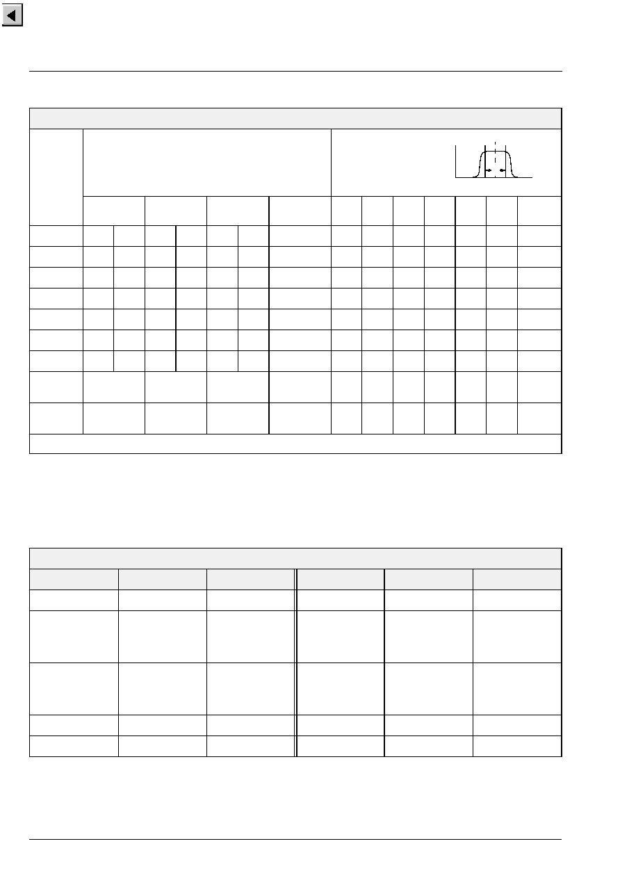
MSP 34x5G
PRELIMINARY DATA SHEET
86
Micronas
Table 6�14: 8-bit FIR-coefficients (decimal integer) for MSP 34x0D; reset status: all coefficients are "0"
Coefficients for FIR1 00 01
hex
and FIR2 00 05
hex
Terrestrial TV Standards
B/G-, D/K-
NICAM-FM
I-
NICAM-FM
L-
NICAM-AM
B/G-, D/K-,
M-Dual FM
130
kHz
180
kHz
200
kHz
280
kHz
380
kHz
500
kHz
Auto-
search
Coef(i)
FIR1
FIR2
FIR1
FIR2
FIR1
FIR2
FIR2
FIR2
FIR2
FIR2
FIR2
FIR2
FIR2
FIR2
0
-
2
3
2
3
-
2
-
4
3
73
9
3
-
8
-
1
-
1
-
1
1
-
8
18
4
18
-
8
-
12
18
53
18
18
-
8
-
9
-
1
-
1
2
-
10
27
-
6
27
-
10
-
9
27
64
28
27
4
-
16
-
8
-
8
3
10
48
-
4
48
10
23
48
119
47
48
36
5
2
2
4
50
66
40
66
50
79
66
101
55
66
78
65
59
59
5
86
72
94
72
86
126
72
127
64
72
107
123
126
126
Mode-
REG[12]
0
0
0
0
1
1
1
1
1
1
0
Mode-
REG[13]
0
0
0
1
1
1
1
1
1
1
0
For compatibility, except for the FIR2-AM and the Autosearch-sets, the FIR-filter programming as used for the MSP 3415B is also possible.
Table 6�15: DCO registers for the MSP 34x5G; reset status: DCO_HI/LO = "0000"
DCO1_LO 00 93
hex
, DCO1_HI 00 9B
hex
; DCO2_LO 00 A3
hex
, DCO2_HI 00 AB
hex
Freq. MHz
DCO_HI/hex
DCO_LO/hex
Freq. MHz
DCO_HI/hex
DCO_LO/hex
4.5
03E8
000
5.04
5.5
5.58
5.7421875
0460
04C6
04D8
04FC
0000
038E
0000
00AA
5.76
5.85
5.94
0500
0514
0528
0000
0000
0000
6.0
6.2
6.5
6.552
0535
0561
05A4
05B0
0555
0C71
071C
0000
6.6
6.65
6.8
05BA
05C5
05E7
0AAA
0C71
01C7
7.02
0618
0000
7.2
0640
0000
7.38
0668
0000
7.56
0690
0000
B
FM - Satellite
FIR filter corresponds to a
band-pass with a band-
width of B = 130 to 500 kHz
f
c
frequency
PRELIMINARY DATA SHEET
MSP 34x5G
Micronas
87
6.4. Manual/Compatibility Mode:
Description of Demodulator Read Registers
Note: The use of these register is no longer recom-
mended. It should be used only in cases where soft-
ware compatibility to the MSP 34x5D is required.
Using the STANDARD SELECTION register together
with the STATUS register provides a more economic
way to program the MSP 34x5G and to retrieve infor-
mation from the IC.
All registers except C_AD_BITs are 8 bit wide. They
can be read out of the RAM of the MSP 34x5G if the
MSP 34x5D compatibility mode is required.
All transmissions take place in 16-bit words. The valid
8-bit data are the 8 LSBs of the received data word.
If the Automatic Sound Select feature is not used, the
NICAM or FM-identification parameters must be read
and evaluated by the controller in order to enable
appropriate switching of the channel select matrix of
the baseband processing part. The FM-identification
registers are described in Section 6.6.1.
To handle the
NICAM-sound and to observe the NICAM-quality, at
least the registers C_AD_BITS and ERROR_RATE
must be read and evaluated by the controller. Addi-
tional data bits and CIB bits, if supplied by the NICAM
transmitter, can be obtained by reading the registers
ADD_BITS and CIB_BITS.
6.4.1. NICAM Mode Control/Additional Data Bits
Register
NICAM operation mode control bits and A[2:0] of the
additional data bits.
Format:
Important: "S" = bit[0] indicates correct NICAM-syn-
chronization (S = 1). If S = 0, the MSP 3415/3455G
has not yet synchronized correctly to frame and
sequence, or has lost synchronization. The remaining
read registers are therefore not valid. The MSP mutes
the NICAM output automatically and tries to synchro-
nize again as long as MODE_REG[6] is set.
The operation mode is coded by C4-C1 as shown in
Table 6�16.
Note: It is no longer necessary to read out and evalu-
ate the C_AD_BITS. All evaluation is performed in the
MSP and indicated in the STATUS register.
6.4.2. Additional Data Bits Register
Contains the remaining 8 of the 11 additional data bits.
The additional data bits are not yet defined by the
NICAM 728 system.
Format:
6.4.3. CIB Bits Register
Cib bits 1 and 2 (see NICAM 728 specifications).
Format:
MSB
C_AD_BITS 00 23
hex
LSB
11
...
7
6
5
4
3
2
1
0
Auto
_FM
...
A[2]
A[1]
A[0]
C4
C3
C2
C1
S
Table 6�16: NICAM operation modes as defined by
the EBU NICAM 728 specification
C4
C3
C2
C1
Operation Mode
0
0
0
0
Stereo sound (NICAMA/B),
independent mono sound (FM1)
0
0
0
1
Two independent mono signals
(NICAMA, FM1)
0
0
1
0
Three independent mono channels
(NICAMA, NICAMB, FM1)
0
0
1
1
Data transmission only; no audio
1
0
0
0
Stereo sound (NICAMA/B), FM1
carries same channel
1
0
0
1
One mono signal (NICAMA). FM1
carries same channel as NICAMA
1
0
1
0
Two independent mono channels
(NICAMA, NICAMB). FM1 carries
same channel as NICAMA
1
0
1
1
Data transmission only; no audio
x
1
x
x
Unimplemented sound coding
option (not yet defined by EBU
NICAM 728 specification)
AUTO_FM: monitor bit for the AUTO_FM Status:
0: NICAM source is NICAM
1: NICAM source is FM
MSB
ADD_BITS 00 38
hex
LSB
7
6
5
4
3
2
1
0
A[10]
A[9]
A[8]
A[7]
A[6]
A[5]
A[4]
A[3]
MSB
CIB_BITS 00 3E
hex
LSB
7
6
5
4
3
2
1
0
x
x
x
x
x
x
CIB1
CIB2
MSP 34x5G
PRELIMINARY DATA SHEET
88
Micronas
6.4.4. NICAM Error Rate Register
Average error rate of the NICAM reception in a time
interval of 182 ms, which should be close to 0. The ini-
tial and maximum value of ERROR_RATE is 2047.
This value is also active if the NICAM bit of
MODE_REG is not set. Since the value is achieved by
filtering, a certain transition time (approx. 0.5 sec) is
unavoidable. Acceptable audio may have error rates
up to a value of 700 int. Individual evaluation of this
value by the controller and an appropriate threshold
may define the fallback mode from NICAM to FM/
AM-mono in case of poor NICAM reception.
The bit error rate per second (BER) can be calculated
by means of the following formula:
BER= ERROR_RATE * 12.3*10
-
6
/s
6.4.5. PLL_CAPS Readback Register
It is possible to read out the actual setting of the
PLL_CAPS. In standard applications, this register is
not of interest for the customer.
6.4.6. AGC_GAIN Readback Register
It is possible to read out the actual setting of
AGC_GAIN in Automatic Gain Mode. In standard
applications, this register is not of interest for the cus-
tomer
.
6.4.7. Automatic Search Function for FM-Carrier
Detection in Satellite Mode
The AM demodulation ability of the MSP 3415G and
MSP 3455G offers the possibility to calculate the "field
strength" of the momentarily selected FM carrier,
which can be read out by the controller. In SAT receiv-
ers, this feature can be used to make automatic FM
carrier search possible.
For this, the MSP has to be switched to AM-mode
(MODE_REG[8]), FM-Prescale must be set to
7F
hex
= +127
dec
, and the FM DC notch (see
Section 6.5.7.)
must be switched off. The sound-IF fre-
quency range must now be "scanned" in the
MSP-channel 2 by means of the programmable
quadrature mixer with an appropriate incremental fre-
quency (i.e. 10 kHz). After each incrementation, a field
strength value is available at the quasi-peak detector
output (quasi-peak detector source must be set to
FM), which must be examined for relative maxima by
the controller. This results in either continuing search
or switching the MSP back to FM demodulation mode.
During the search process, the FIR2 must be loaded
with the coefficient set "AUTOSEARCH", which
enables small bandwidth, resulting in appropriate field
strength characteristics. The absolute field strength
value (can be read out of "quasi peak detector output
FM1") also gives information on whether a main FM
carrier or a subcarrier was detected; and as a practical
consequence, the FM bandwidth (FIR1/2) and the
deemphasis (50
�
s or adaptive) can be switched
accordingly.
Due to the fact that a constant demodulation frequency
offset of a few kHz, leads to a DC level in the demodu-
lated signal, further fine tuning of the found carrier can
be achieved by evaluating the "DC Level Readout
FM1". Therefore, the FM DC Notch must be switched
on, and the demodulator part must be switched back to
FM-demodulation mode.
For a detailed description of the automatic search
function, please refer to the corresponding MSP Win-
dows software.
ERROR_RATE
00 57
hex
Error free
0000
hex
maximum error rate
07FF
hex
PLL_CAPS
02 1F
hex
L
minimum frequency
1111 1111
FF
hex
nominal frequency
0101 0110
56
hex
RESET
maximum frequency
0000 0000
00
hex
PLL_CAPS
02 1F
hex
H
PLL open
xxxx xxx0
PLL closed
xxxx xxx1
AGC_GAIN
02 1E
hex
max. amplification
(20 dB)
0001 0100
14
hex
min. amplification
(3 dB)
0000 0000
00
hex
PRELIMINARY DATA SHEET
MSP 34x5G
Micronas
89
6.5. Manual/Compatibility Mode:
Description of DSP Write Registers
6.5.1. Additional Channel Matrix Modes
This table shows more modes for the channel matrix
registers.
The sum/difference mode can be used together with
the quasi-peak detector to determine the sound mate-
rial mode. If the difference signal on channel B (right)
is near to zero, and the sum signal on channel A (left)
is high, the incoming audio signal is mono. If there is a
significant level on the difference signal, the incoming
audio is stereo.
6.5.2. Volume Modes of SCART1 Output
6.5.3. FM Fixed Deemphasis
Note: This register is initialized during STANDARD
SELECTION and is automatically updated when Auto-
matic Sound Select (MODUS[0]=1) is on.
6.5.4. FM Adaptive Deemphasis
Note: This register is initialized during STANDARD
SELECTION and is automatically updated when Auto-
matic Sound Select (MODUS[0]=1) is on.
6.5.5. NICAM Deemphasis
A J17 Deemphasis is always applied to the NICAM sig-
nal. It is not switchable.
Loudspeaker Matrix
00 08
hex
L
SCART1 Matrix
00 0A
hex
L
I
2
S Matrix
00 0B
hex
L
Quasi-Peak
Detector Matrix
00 0C
hex
L
SUM/DIFF
0100 0000
40
hex
AB_XCHANGE
0101 0000
50
hex
PHASE_CHANGE_B
0110 0000
60
hex
PHASE_CHANGE_A
0111 0000
70
hex
A_ONLY
1000 0000
80
hex
B_ONLY
1001 0000
90
hex
Volume Mode SCART1
00 07
hex
[3:0]
linear
0000
0
hex
RESET
logarithmic
0001
1
hex
Linear Mode
Volume SCART1
00 07
hex
H
OFF
0000 0000
00
hex
RESET
0 dB gain
(digital full scale (FS) to 2
V
RMS
output)
0100 0000
40
hex
+6 dB gain (
-
6 dBFS to 2
V
RMS
output)
0111 1111
7F
hex
FM Deemphasis
00 0F
hex
H
50
�
s
0000 0000
00
hex
RESET
75
�
s
0000 0001
01
hex
J17
0000 0100
04
hex
OFF
0011 1111
3F
hex
FM Adaptive
Deemphasis WP1
00 0F
hex
L
OFF
0000 0000
00
hex
RESET
WP1
0011 1111
3F
hex
MSP 34x5G
PRELIMINARY DATA SHEET
90
Micronas
6.5.6. Identification Mode for A2 Stereo Systems
To shorten the response time of the identification algo-
rithm after a program change between two FM-Stereo
capable programs, the reset of the ident-filter can be
applied.
Sequence:
1. Program change
2. Reset ident-filter
3. Set identification mode back to standard B/G or M
4. Wait approx. 500 ms
5. Read stereo detection register
Note: This register is initialized during STANDARD
SELECTION and is automatically updated when Auto-
matic Sound Select (MODUS[0]=1) is on.
6.5.7. FM DC Notch
The DC compensation filter (FM DC Notch) for FM
input can be switched off. This is used to speed up the
automatic search function (see Section 6.4.7.). In nor-
mal FM-mode, the FM DC Notch should be switched
on.
6.6. Manual/Compatibility Mode:
Description of DSP Read Registers
All readable registers are 16-bit wide. Transmissions
via I
2
C bus have to take place in 16-bit words. Some of
the defined 16-bit words are divided into low and high
byte, thus holding two different control entities.
These registers are not writable.
6.6.1. Stereo Detection Register
for A2 Stereo Systems
Note: It is no longer necessary to read out and evalu-
ate the A2 identification level. All evaluation is per-
formed in the MSP and indicated in the STATUS regis-
ter.
6.6.2. DC Level Register
The DC level register measures the DC component of
the incoming FM signals (FM1 and FM2). This can be
used for seek functions in satellite receivers and for IF
FM frequencies fine tuning. A too low demodulation
frequency (DCO) results in a positive DC-Level and
vice versa. For further processing, the DC content of
the demodulated FM signals is suppressed. The time
constant
,
defining the transition time of the DC Level
Register, is approximately 28 ms.
Identification Mode
00 15
hex
L
Standard B/G
(German Stereo)
0000 0000
00
hex
RESET
Standard M
(Korean Stereo)
0000 0001
01
hex
Reset of Ident-Filter
0011 1111
3F
hex
FM DC Notch
00 17
hex
L
ON
0000 0000
00
hex
Reset
OFF
0011 1111
3F
hex
Stereo Detection
Register
00 18
hex
H
Stereo Mode
Reading
(two's complement)
MONO
near zero
STEREO
positive value (ideal
reception: 7F
hex
)
BILINGUAL
negative value (ideal
reception: 80
hex)
DC Level Readout
FM1 (MSP-Ch2)
00 1B
hex
H+L
DC Level Readout
FM2 (MSP-Ch1)
00 1C
hex
H+L
DC Level
[8000
hex
... 7FFF
hex
]
values are 16 bit two's
complement

PRELIMINARY DATA SHEET
MSP 34x5G
Micronas
91
6.7. Demodulator Source Channels in Manual Mode
6.7.1. Terrestric Sound Standards
Table 6�17 shows the source channel assignment of
the demodulated signals in case of manual mode for
all terrestric sound standards. See Table 2�2 for the
assignment in the Automatic Sound Select mode. In
manual mode for terrestric sound standards, only two
demodulator sources are defined.
6.7.2. SAT Sound Standards
Table 6�18 shows the source channel assignment of
the demodulated signals for SAT sound standards.
6.8. Exclusions of Audio Baseband Features
In general, all functions can be switched independently.
Two exceptions exist:
1. NICAM cannot be processed simultaneously with
the FM2 channel.
2. FM adaptive deemphasis cannot be processed
simultaneously with FM-identification.
6.9. Compatibility Restrictions to MSP 34x5D
The MSP 34x5G is fully hardware compatible to the
MSP 34x5D. However, to substitute a MSP 34x5D by
the corresponding MSP 34x5G, the controller software
has to be adapted slightly:
1. The register FM-Matrix (00 0E
hex
low part) must be
changed from "no matrix (00
hex
)" to "sound A mono
(03
hex
)" during mono transmission of all TV-sound
standards (see also Table 6�17).
2. With the MSP 34x5G, the STANDARD SELECTION
initializes the FM-deemphasis, which is not the case
for the MSP 34x5D. So, if STANDARD SELECTION
is applied, this I
2
C instruction can be omitted.
MSP 34x5G
PRELIMINARY DATA SHEET
92
Micronas
Table 6�17: Manual Sound Select Mode for Terrestric Sound Standards
Source Channels of Sound Select Block
Broadcasted
Sound
Standard
Selected MSP
Standard
Code
Broadcasted
Sound Mode
FM Matrix
FM/AM
(use 0 for channel select)
Stereo or A/B
(use 1 for channel select)
B/G-FM
D/K-FM
M-Korea
M-Japan
03
04, 05
02
30
MONO
Sound A Mono
Mono
Mono
STEREO
German Stereo
Korean Stereo
Stereo
Stereo
BILINGUAL,
Languages A and B
No Matrix
Left = A
Right = B
Left = A
Right = B
B/G-NICAM
L-NICAM
I-NICAM
D/K-NICAM
D/K-NICAM
(with high
deviation FM)
08
09
0A
0B
0C
0D
NICAM not available
or NICAM error rate
too high
Sound A Mono
1)
analog Mono
no sound
with AUTO_FM:
analog Mono
MONO
Sound A Mono
1)
analog Mono
NICAM Mono
STEREO
Sound A Mono
1)
analog Mono
NICAM Stereo
BILINGUAL,
Languages A and B
Sound A Mono
1)
analog Mono
Left = NICAM A
Right = NICAM B
BTSC
20
MONO
Sound A Mono
Mono
Mono
STEREO
Korean Stereo
Stereo
Stereo
MONO
+
SAP
Sound A Mono
Mono
Mono
STEREO
+
SAP
Korean Stereo
Stereo
Stereo
21
MONO
Sound A Mono
Mono
Mono
STEREO
MONO
+
SAP
No Matrix
Left = Mono
Right = SAP
Left = Mono
Right = SAP
STEREO
+
SAP
FM-Radio
40
MONO
Sound A Mono
Mono
Mono
STEREO
Korean Stereo
Stereo
Stereo
1)
Automatic refresh to Sound A Mono, do not write any other value to the register FM Matrix!
Table 6�18: Manual Sound Select Modes for SAT-Standards
Source Channels of Sound Select Block for SAT-Modes
Broadcasted
Sound
Standard
Selected
MSP Standard
Code
Broadcasted
Sound Mode
FM Matrix
FM/AM
(source select: 0)
Stereo or A/B
(source select: 1)
Stereo or A
(source select: 3)
Stereo or B
(source select: 4)
FM SAT
6, 50
hex
MONO
Sound A Mono
Mono
Mono
Mono
Mono
51
hex
STEREO No
Matrix
Stereo
Stereo
Stereo
Stereo
BILINGUAL
No Matrix
Left = A (FM1)
Right = B (FM2)
Left = A (FM1)
Right = B (FM2)
A (FM1)
B (FM2)

PRELIMINARY DATA SHEET
MSP 34x5G
Micronas
93
7. Appendix D: Application Information
7.1. Phase Relationship of Analog Outputs
The user does not need to correct output phases when
using the loudspeaker output directly. The SCART1
output has opposite phase.
The following schematics shows the phase relation-
ship of all analog inputs and outputs.
Fig. 7�1: Phase diagram of the MSP 34x5G
SCART1
SCART1
SCART2
MONO
Loudspeaker
SCART1-Ch.
MONO, SCART1...2
SCART
DSP
Input
Select
SCART
Output Select
Audio
Baseband
Processing

MSP 34x5G
PRELIMINARY DATA SHEET
94
Micronas
7.2. Application Circuit
SC1_OUT_L
SC1_OUT_R
AHV
S
UP
AHV
S
S
AV
SUP
DVS
U
P
DVS
S
AV
SS
VRE
F
1
VRE
F
2
5 V
5 V
8 V
AVS
S
5 V
5 V
CAP
L
_
M
VR
E
F
T
O
P
AGNDC
ANA
_
I
N
1
+
AN
A
_
I
N
-
XTA
L
_
I
N
X
T
A
L_OU
T
MSP 34x5G
D_CTR_I/O_0
D_CTR_I/O_1
TESTEN
100
100
22
�
F
22
�
F
+
+
1 nF
1 nF
DACM_R
DACM_L
1
�
F
1
�
F
Loudspeaker
Tuner
Signal GND
SIF 1 IN
56 pF
56 pF
+
3.3
�
F
100
nF
100
nF
10
�
F
+
-
8 V (5 V)
18.432
MHz
+
10
�
F
MONO_IN
SC1_IN_L
SC1_IN_R
ASG
SC2_IN_L
SC2_IN_R
STANDBYQ
ADR_SEL
I2C_DA
I2C_CL
220
pF
Alternative circuit for
SIF-input for more
attenuation of video
100 p
56 p
1 k
ANA_IN1+
AHVSS
330 nF
330 nF
330 nF
330 nF
330 nF
DVSS
DVSS
AHVSS
components:
C s. section 4.6.2.
RESETQ
(from Controller, see section 4.6.3.3.)
1.5
nF
470
pF
10
�
F
1.5
nF
470
pF
10
�
F
1.5
nF
470
pF
10
�
F
ADR_WS
ADR_CL
ADR_DA
I2S_WS
I2S_CL
I2S_DA_IN1
I2S_DA_IN2
I2S_DA_OUT
(5 V)
AHVS
S
AHVS
S
AHVS
S
RES
E
T
Q

PRELIMINARY DATA SHEET
MSP 34x5G
Micronas
95

All information and data contained in this data sheet are without any
commitment, are not to be considered as an offer for conclusion of a
contract, nor shall they be construed as to create any liability. Any new
issue of this data sheet invalidates previous issues. Product availability
and delivery are exclusively subject to our respective order confirmation
form; the same applies to orders based on development samples deliv-
ered. By this publication, Micronas GmbH does not assume responsibil-
ity for patent infringements or other rights of third parties which may
result from its use.
Further, Micronas GmbH reserves the right to revise this publication
and to make changes to its content, at any time, without obligation to
notify any person or entity of such revisions or changes.
No part of this publication may be reproduced, photocopied, stored on a
retrieval system, or transmitted without the express written consent of
Micronas GmbH.
MSP 34x5G
PRELIMINARY DATA SHEET
96
Micronas
Micronas GmbH
Hans-Bunte-Strasse 19
D-79108 Freiburg (Germany)
P.O. Box 840
D-79008 Freiburg (Germany)
Tel. +49-761-517-0
Fax +49-761-517-2174
E-mail: docservice@micronas.com
Internet: www.micronas.com
Printed in Germany
Order No. 6251-480-3PD
8. Appendix E: MSP 34x5G Version History
MSP 3435G-A2
First release for BTSC-Stereo/SAP and FM-Radio.
MSP 34x5G-B5
� additional package PLQFP64
� digital input specification changed as of version B5
and later (see Section 4.6. on page 53)
� max. analog high supply voltage AHVSUP 8.7 V.
� supply currents changed as of version B5 and later
(see Section 4.6.3. on page 58)
� programmable A2 and carrier mute thresholds
� new D/K standard 0D
hex
: HDEV3 and NICAM
� additional preference in Automatic Standard Detec-
tion
MSP 34x5G-B6
� improved AM-performance (see page 69)
� new D/K standard for Poland
(see Table 3�7 on page 20)
� improved I
2
C hardware problem handling
(see Section 3.1.1. on page 15)
� faster system-D/K-loop for stereo detection
� extended features in the CONTROL register
(see Section 3.1.2. on page 16)
MSP 34x5G-B8
� fine-tuning of A2-identification and carrier mute
� EIA-J identification: faster transition time stereo/
bilingual to mono
� J17 FM-deemphasis implemented
� input specification for RESETQ and TESTEN
changed
9. Data Sheet History
1. Preliminary data sheet: "MSP 34x5G Multistandard
Sound Processor Family, Edition Oct. 26, 1998, 6251-
480-1PD. First release of the preliminary data sheet.
2. Preliminary data sheet: "MSP 34x5G Multistandard
Sound Processor Family", Edition July 11, 2000, 6251-
480-2PD. Second release of the preliminary data
sheet. Major changes:
� section Specifications: specification for PLQFP64
package added
� specification for version B5 and B6 added
(see Appendix E: Version History)
� reset description modified
� I
2
S and ADR functionality added
� MSP 3425G and MSP 3465G added
� Multistandard controller software flow diagram
added
3. Preliminary data sheet: "MSP 34x5G Multistandard
Sound Processor Family", March 5, 2001, 6251-480-
3PD. Third release of the preliminary data sheet. Major
changes:
� Section 4.2.: pin allocation for PLQFP64 corrected
� I
2
C-bus description changed
� ACB register: documentation for bit allocation
D_CTR_I/O changed

Micronas
97
Micronas
page 1 of 1
Subject:
Data Sheet Concerned:
Supplement:
Edition:
Preliminary Data Sheet Supplement
Version Changes within the MSP 34xxG Family:
For a detailed description of the below-mentioned items, see the corresponding data sheets. For quick reference,
check the version history in the data sheet appendices.
MSP 34x0G
A4
B4
B5
B6
B8
MSP 34x1G
A1
A2
B8
MSP 34x2G
A1
MSP 34x5G
A4
B5
B6
B8
MSP 34x7G
B6
B8
technology
0.8 �
0.5 �
0.5 �
0.5 �
0.45 �
power dissipation (typical) at 8 V operation
MSP 34x0/x1/x5/x7
MSP 34x2
740 mW 640 mW 640 mW 640 mW
690 mW
600 mW
digital input specification change
x
x
x
specification of max. analog high voltage (AHVSUP)
8.4 V
8.4 V
8.7 V
8.7 V
8.7 V
programmable A2 and carrier mute thresholds
x
x
x
new Standard Select Mode 0D
hex
: D/K-NICAM together with HDEV3 FM mode
x
x
x
additional preference "color" for 4.5 MHz carrier in Automatic Standard Detection
x
x
x
improved AM-performance (better SNR and THD)
x
x
new Standard Select Mode 07
hex
: D/K3 for Poland
x
x
faster system D/K loop for stereo detection (standards 4, 5, 7, B with ASS = on)
x
x
improved I
2
C hardware problem handling
x
x
extended features in the CONTROL register (readout hardware / reset status)
x
x
Micronas Dynamic Bass (MDB)
MSP 34x0/x1/x2
x
x
Micronas Dynamic Bass (improved MDB)
MSP 34x0/x1/x2
x
faster identification for all standards, major speedup of
identification for EIA-J standard
x
faster carrier mute
x
J17 deemphasis
x
MSP 34xxG Version History
All MSP 34xxG Data Sheets
No. 2/ 6251-525-2PDS
Oct. 11, 2000
MSP 34xxG