 | –≠–ª–µ–∫—Ç—Ä–æ–Ω–Ω—ã–π –∫–æ–º–ø–æ–Ω–µ–Ω—Ç: OL2068 | –°–∫–∞—á–∞—Ç—å:  PDF PDF  ZIP ZIP |
Applications
∑
Industrial encoder interfacing
∑
Industrial sensor interfacing
∑
Proximity switches
∑
Industrial controllers
∑
Light barriers
Features
∑ Ultra small package TSSOP 20
∑ Max. voltage range from 4,5 V ≠ 36 V
∑ Short circuit proof tri-state outputs drive up to 120mA
sink / source
∑ Operating frequency up to 4 MHz
∑ Integrated voltage reg. with 5V output
∑ Dynamic peak current up to 1,5 Amp.
∑ High impedance CMOS / TTL compatible buffered
inputs with hysteresis
∑ Outputs RS422A compatible
Ultra small package TSSOP 20
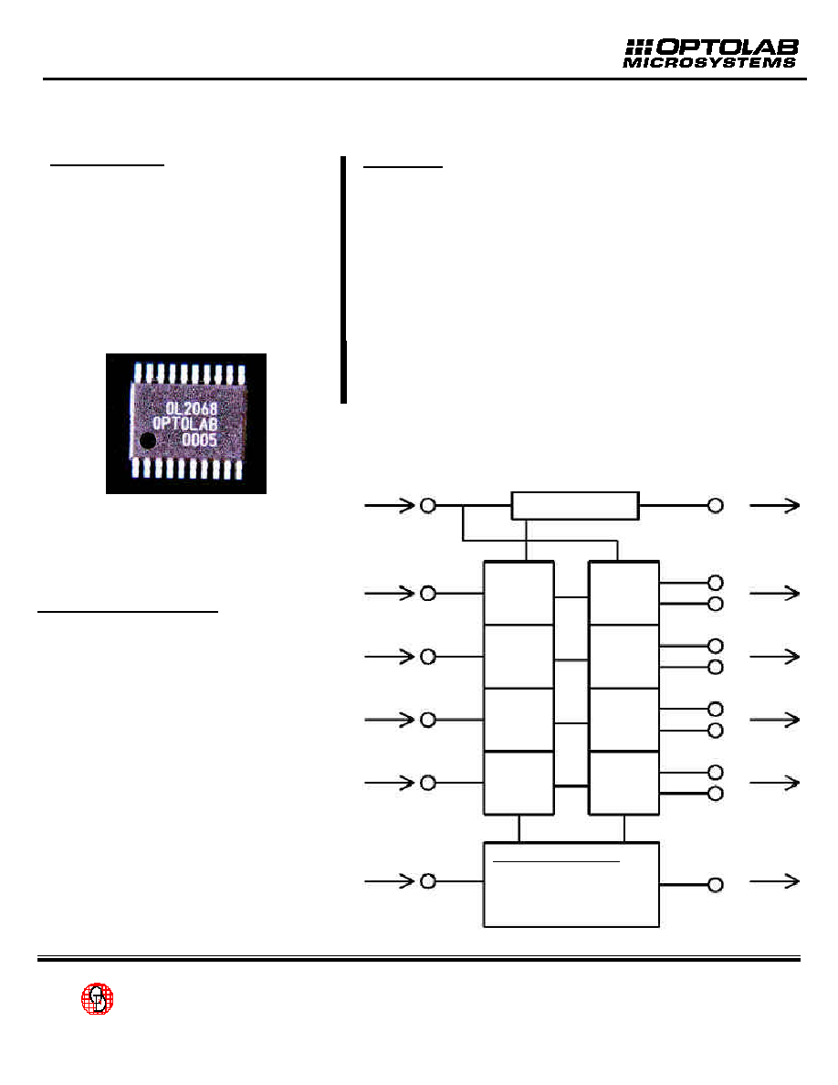
General Description
The OL2068 is an industrial power line
driver and contains four identical short cir-
cuit proof differential line drivers up to 30
Volts driver supply with a joint enable func-
tion. An internal 5 V power supply is used
as reference and supply voltage for the
circuitry and is able to supply max. 5mA
for external 5V components like a sensor
or a constant current source for an LED.
The very small outline TSSOP package
gives excellent thermal power dissipation,
thus the usage in space limited applica-
tions is easy.
OL2068
Industrial 30 Volt 4-Channel Differential Power Line Driver - Short Circuit Proof -
Line voltage in
Voltage regulator
5V , 5mA out
CMOS / TTL
Data input
Differential
Output A
Output A-
Differential
Output B
Output B-
Differential
Output C
Output C-
Differential
Output D
Output D-
Tristate enable / disable
Thermal shutdown disable
Protection logic controller
- short circuit shut down
- Tristate and thermal logic control
- Undervoltage and power up reset
- Transient and EMI protection
CMOS / TTL
Data input
CMOS / TTL
Data input
CMOS / TTL
Data input
Error signal out
For Stateside information contact...
Quantum Devices, Inc., 112 Orbison St., PO Box 100, Barneveld, WI, 53507
q
Tele: (608) 924-3000 qFax: (608) 924-3007 qURL: www.quantumdev.com qEmail: qdisales@quantumdev.com

Table 1 Absolute Maximum Ratings
OL2068
Industrial 30 Volt 4-Channel Differential Power Line Driver - Short Circuit Proof -
Electrical characteristics
All voltage values are referenced to GND (GND = 0V).
Unless stated otherwise all signals are assumed to be high active.
Table 2 Recommended Operating Conditions
NOTE:Stresses above those listed under "Absolute Maximum Ratings" may cause permanent damage to the device. This is a stress
rating only and functional operation of the device at these or any other conditions above those indicated in the operational section of this
specification is not implied. Exposure to absolute maximum rating conditions for extended periods may affect device reliability (eq. hot
carrier degradation).
For Stateside information contact...
Quantum Devices, Inc., 112 Orbison St., PO Box 100, Barneveld, WI, 53507
q
Tele: (608) 924-3000 qFax: (608) 924-3007 qURL: www.quantumdev.com qEmail: qdisales@quantumdev.com
Parameter
Symbol Condition
Min
Max
Unit
DC supply voltage
V
CCD
-0.3
36.0
V
DC input voltage
V
IN
-0.3
V
CC
+0.3
V
DC input current
I
In
±10
mA
Output voltage
V
OUT
-0.3
V
CC
+0.3
V
Driver output current (see cable model)
I
OUT
pulse peak/average
1500/100
mA
Storage and operating temperature range
T
STGOP
-55
+125
∞C
Junction temperature
T
J
+150
1
∞C
Lead temperature
T
L
soldering, 10s
+260
2
∞C
Power dissipation:
OL7272 SOIC16NB: R
thj-
a
=111.8 K/W
OL2068 TSSOP20: R
thj-
a
= 81.4 K/W
PD
still air,
T
A
=85∞C,
T
J
=150∞C
581
798
mW
mW
Parameter
Symbol
Condition
Min
Max
Unit
DC supply voltage
V
CCD
4.5
30.0
V
DC data input voltage
V
IN
D
0
V
CCD
V
DC enable input voltage
V
IN
EN
3
0
5.5
V
Data output voltage
V
OUT
D
0
V
CCD
V
TMON output voltage
V
OUT
TM
0
V
CCI
V
Driver output current (see cable model)
I
OUT
4
100
mA
Operating ambient temperature range
T
A
5
-40
+100
∞C
Junction temperature range (lifetime)
T
J
-55
+125
∞C
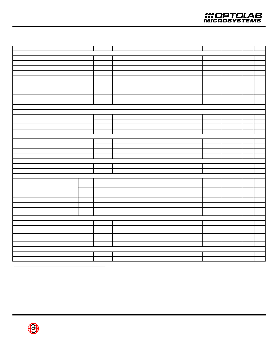
Table 3 DC Characteristics (V
CCD
= 12.0 V, T
A
= 25 ∞C, unless otherwise noted)
OL2068
Industrial 30 Volt 4-Channel Differential Power Line Driver - Short Circuit Proof -
6
Either the low or high side switch is active at a time.
7
Values will not be part of the production test but guaranteed by design.
8
Output MON external driving current up to 4mA possible - but using this limits the thermal power budget!
9
Measured without external load on V
CCI
pin, all outputs open.
10
For decoupling V
CCI
please connect this output with a 100nf capacitor to GND
11
Depends on supply voltage V
CCD
, V
CCI
could be not higher than V
CC
- 0.3 V.
12
This is measured per input with all other inputs held at VCCI or GND.
13
Limited by power dissipation, high I
CCI
current with growing V
CCD
voltage generates heat, thus the driving limit can be reached earlier.
14
Value will not be part of the production test but guaranteed by design.
For Stateside information contact...
Quantum Devices, Inc., 112 Orbison St., PO Box 100, Barneveld, WI, 53507
q
Tele: (608) 924-3000 qFax: (608) 924-3007 qURL: www.quantumdev.com qEmail: qdisales@quantumdev.com
Paramter
Symbol
Condition
Min
Typ
Max
Unit
Schmitt trigger inputs section
Data input hysteresis
V
HYS
D
V
IL
to V
IH
and V
IH
to V
IL
, ENABLE <= 0.8 V
0.2
0.5
V
Data input positive going threshold
V
TH+
D
ENABLE <= 0.8 V
1.7
2.4
V
Data input negative going threshold
V
TH-
D
ENABLE <= 0.8 V
0.8
1.2
V
Enable input hysteresis
V
HYS
EN
V
IL
to V
IH
and V
IH
to V
IL
,
0.2
0.5
V
Enable input pos. going threshold
V
TH+
EN
1.7
2.4
V
Enable input neg. going threshold
V
TH-
EN
0.8
1.2
V
Data input leakage current -Low
I
IL
D
ENABLE <= 0.8 V
-10.0
+10.0
µA
-High
I
IH
D
ENABLE <= 0.8 V
-10.0
+10.0
µA
Enable input leakage current -Low
I
IL
EN
-10.0
+10.0
µA
-High
I
IH
EN
-10.0
+10.0
µA
Push-pull output drive section
- Low side switch outputs
6
Low level output voltage
V
OLB
V
CCD
= 4.75 V, I
LOAD
= 20 mA, ENABLE <= 0.08 V
0.3
0.5
V
V
OLT
V
CCD
= 30 V, I
LOAD
= 30mA, ENABLE <= 0.08 V
0.4
0.5
V
Output resistance
R
DSON
I
LOAD
= 30mA
13
20
High-impedance output leakage current
I
OZ
V
CCD
= 30.0 V, ENABLE >= 2.4 V
-10.0
+10.0
µA
- High side switch ouptuts
6
High level output voltage
V
OHB
V
CCD
= 4.75 V, I
LOAD
= -20mA, ENABLE <=0.80 V
4.2
V
CCD
-0.4
V
V
OHT
V
CCD
= 30V, I
LOAD
= 30mA, ENABLE <=0.8 V
29.2
V
CCD
-0.6
V
Output resistance
R
DSON
I
LOAD
= 30mA
20
30
High-impedance output leakage current
I
OZ
V
CCD
= 30.0 V, ENABLE >= 2.4 V
-10.0
+10.0
µA
-MON output
8
Low level output voltage
V
OL
I
LOAD
= 2.0 mA
0.4
V
High level output voltage
V
OH
I
LOAD
= 2.0mA
V
CCI
-0.8
V
Supply parameters section
V
CCD
supply current
9
I
DB
(en)
V
CCD
= 5.0 V, ENABLE <= 0.8 V
1.5
5.0
mA
I
DT
(en)
V
CCD
= 30.0 V, ENABLE <= 0.8 V
1.5
5.0
mA
I
DB
(dis)
V
CCD
= 5.0 V, ENABLE >= 2.4 V
1.5
3.0
mA
I
DT
(dis)
V
CCD
= 30.0 V, ENABLE >= 2.4 V
1.5
3.0
mA
Internal supply voltage
10
V
CCI
11
I
CCIE
= 5.0 mA
4.5
5.0
5.5
V
Quiescent current
I
CCQ
12
V
IN
= 2.4 V OR 0.8 V
0.2
mA
Current from internal voltage
regulator to supply external devices
I
CCIE
13
5.0
mA
Low voltage reset section
Hysteresis for under-voltage reset
V
HYS
LVR
0.1
V
Under-votlage reset negative going threshold
(active)
V
TH
-LVR
3.3
3.5
3.7
V
Under-voltage reset positive going threshold
(inactive)
V
TH+
LVR
3.4
3.6
3.8
V
Under-voltage reset filter time
t
FIL
LVR
14
5
µs
Over-temperature protection section
Over-temp. operate point (junction)
T
JOP
+165
+185
∞C
Over-temp. release point (junction)
T
JRP
+125
+135
∞C
OL2068
Industrial 30 Volt 4-Channel Differential Power Line Driver - Short Circuit Proof -
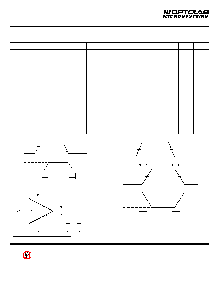
Table 4 AC Characteristics (V
CCD
= 12.0 V, T
A
= 25 ∞C,
Cable capacitance 1000pF
, unless otherwise noted)
15
Measured from 10% to 90% of the Output signal with a capacitive load on each output pin to ground (see Figure 3).
Figure 2
Definition of Output Rise and Fall Time
Figure 3
AC Test Circuit
C
L
= 1.000pF
Figure 1
Timing diagram with typical asynchronous
propagation delays
V
OL
V
OH
Input
Output
V
TH+
V
IH
V
IL
V
TH-
90%
10%
10%
90%
t
R
t
F
50%
50%
50%
50%
V
OL
V
OH
Input
Output
Output-
t
PLH
t
PHL
t
PHL
50%
50%
V
IH
V
IL
t
PLH
V
OL
V
OH
V
CCD
Output+
Output-
1/4
OL2068
Input
C
L
C
L
For Stateside information contact...
Quantum Devices, Inc., 112 Orbison St., PO Box 100, Barneveld, WI, 53507
q
Tele: (608) 924-3000 qFax: (608) 924-3007 qURL: www.quantumdev.com qEmail: qdisales@quantumdev.com
Paramter
Symbol
Condition
Min
Typ
Max
Unit
Disable delay time
t
O F F
100
200.0
ns
Enable delay time
t
O N
76
600.0
ns
Propagation delay from 50% point of
rising edge of input pulse to zero crossing
of differential outputs (see figure 1)
t
PLH
V
CCD
= 5.0 V
V
CCD
= 12.0 V
V
CCD
= 24.0 V
C
LOAD
= 1000 pF
64
74
100
200.0
200.0
330.0
ns
ns
ns
Propagation delay from 50% point of
falling edge of input pulse to zero crossing
of differential outputs (see figure 1)
t
PHL
V
CCD
= 5.0 V
V
CCD
= 12.0 V
V
CCD
= 24.0 V
C
LOAD
= 1000 pF
70
80
100
280.0
280.0
330.0
ns
ns
ns
Output rise time (see figure 2)
t
R
15
V
CCD
= 5.0 V
V
CCD
= 12.0 V
V
CCD
= 24.0 V
C
LOAD
= 1000 pF
42
110
120
200.0
350.0
380.0
ns
ns
ns
Output fall time (see figure 2)
t
F
16
V
CCD
= 5.0 V
V
CCD
= 12.0 V
V
CCD
= 24.0 V
C
LOAD
= 1000 pF
32
62
84
200.0
350.0
380.0
ns
ns
ns
OL2068
Industrial 30 Volt 4-Channel Differential Power Line Driver - Short Circuit Proof -
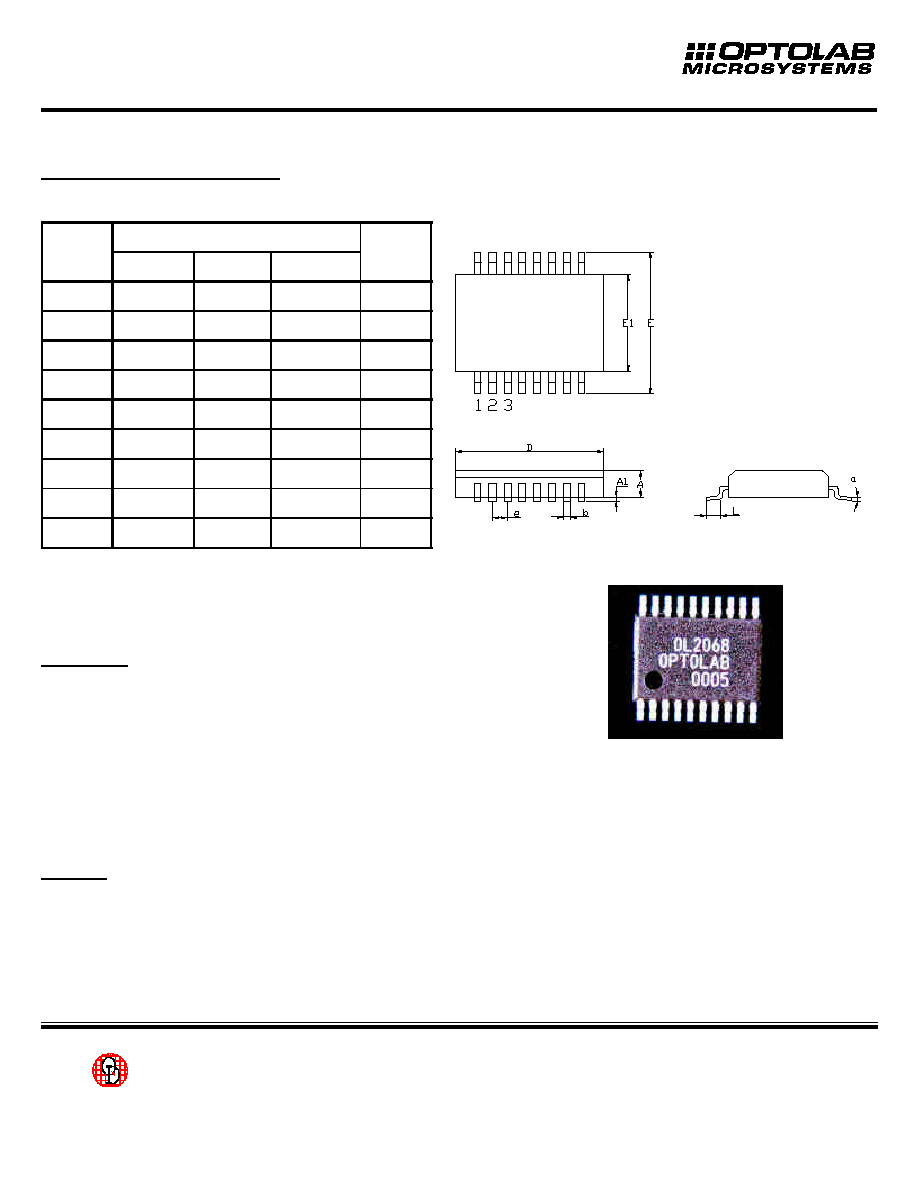
Mechanical characteristics
Package Dimensions
Form of delivery and order code
TSSOP20
Antistatic tubes containing 70pcs order part no. OL2068
Tape & Reel part no. OL2068 TR
High thermal power dissipation by integrated heatlink append "HL" to part number.
A demoboard with 2 line drivers plus connectors and status LEDs is available with order code
OL2068 Demo
Notes:
For hybrid applications this driver is also available as chip. Please contact us for further details.
For space critical applications custom design packages, i.e. with 2 or more driver chips in one package, can
be designed at customer request. Please email Quantum Devices, Inc. at qdisales@quantumdev.com
For Stateside information contact...
Quantum Devices, Inc., 112 Orbison St., PO Box 100, Barneveld, WI, 53507
q
Tele: (608) 924-3000 qFax: (608) 924-3007 qURL: www.quantumdev.com qEmail: qdisales@quantumdev.com
Symbol
TSSOP20(173 mil)
Unit
Min
Typ
Max
D
6.40(0,25)
-
6.60(0,26)
mm(inch)
E1
4.30(0,17)
-
4.50(0,18)
mm(inch)
E
-
6.40(0,25)
-
mm(inch)
A
-
-
1.20(47)
mm(mils)
A1
0.05(2)
-
0.15(6)
mm(mils)
b
0.19(7)
-
0.30(11)
mm(mils)
e
-
0.65(26)
-
mm(mils)
L
0.50(20)
-
0.75(30)
mm(mils)
-
8
-
o