 | –≠–Ľ–Ķ–ļ—ā—Ä–ĺ–Ĺ–Ĺ—č–Ļ –ļ–ĺ–ľ–Ņ–ĺ–Ĺ–Ķ–Ĺ—ā: OLF100 | –°–ļ–į—á–į—ā—Ć:  PDF PDF  ZIP ZIP |
Description
Features
ISO
LINK
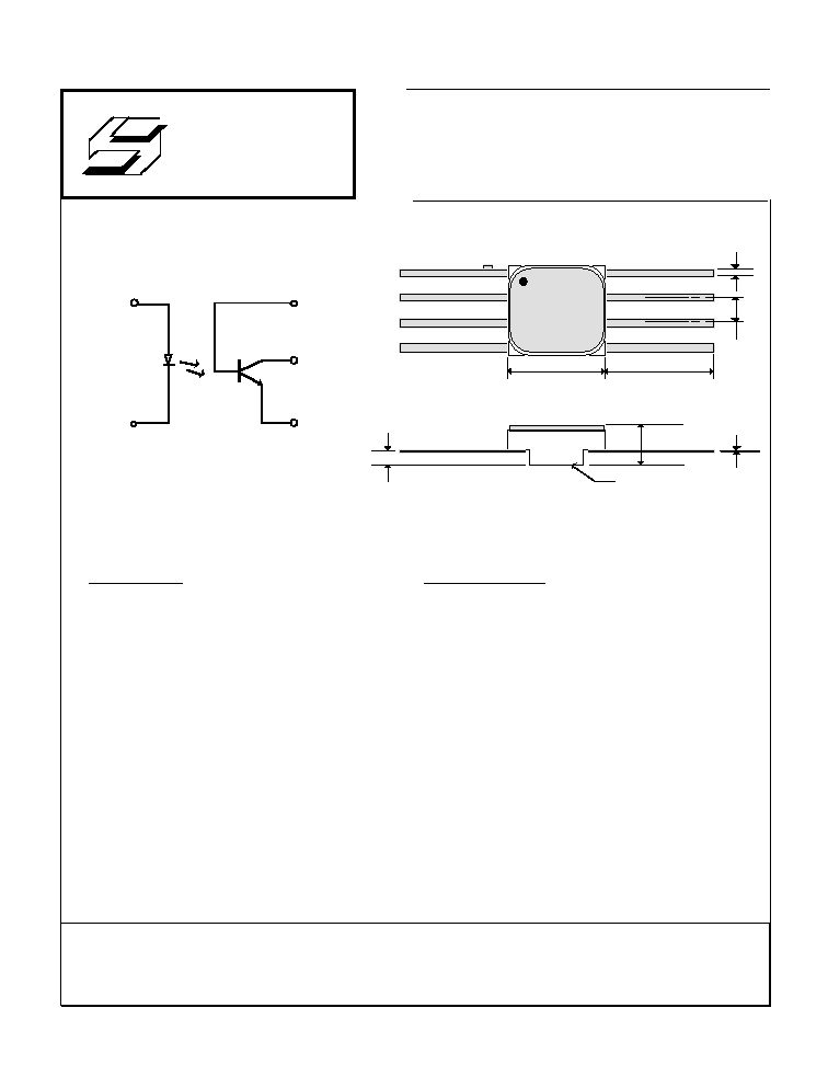
SCHEMATIC
PACKAGE OUTLINE
1. Measured between pins 1, 2 , 3 and 4 shorted together and pins 5, 6, 7 and 8 shorted together. TA = 25
į
C and duration = 1 second.
2. Derate linearly to 125
į
C free-air temperature at 0.67 mA /
į
C above 65
į
C.
3. For pulse width
1
Ķ
S, pulse repetition rate
300 pps.
4. Derate linearly to 125
į
C free-air temperature at 3.0 mW /
į
C above 25
į
C
NOTES:
OLF100
Phototransistor
Hermetic Surface Mount
Optocoupler
The OLF 100 consists of a light
emitting diode optically coupled to a NPN
silicon phototransistor mounted in a 8-pin
hermetic surface mount flat pack package.
The leads can be formed to provide compli-
ant solder connections to the mounting
substrate.
Special electrical parametric selections
are availabe on request.
1
2
3
4
5
6
7
8
.015Ī.002
.050 BSC
.180 SQ. MAX
.200 MIN.
.004/.006
.100 MAX.
.030Ī.005
SEATING PLANE
OLF XXX
XXYY
S
1
2
6
7
CATHODE
ANODE
5
BASE
COLLECTOR
EMITTER
Hermetic SMT package
Compliant surface mounting leads
High current transfer ratio
Small package size
High reliability and rugged construction
100% hi-rel screenings are offered
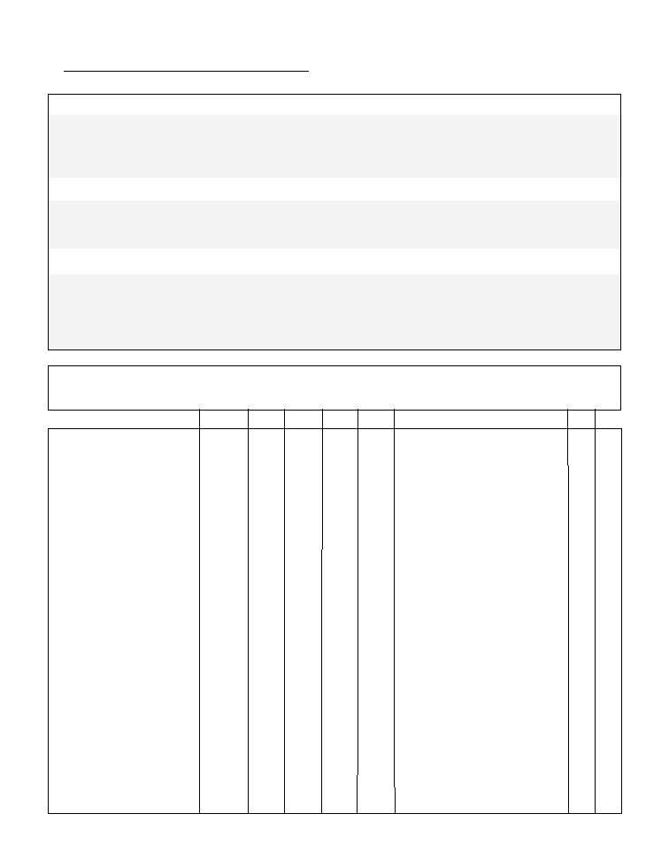
ELECTRICAL CHARACTERISTIC ( T
A
= - 55
į
C to +125
į
C, Unless Otherwise Specified )
Parameter
Symbol Min Typ. Max Units Test Conditions Fig. Note
ALL TYPICAL @ T
A
= 25
į
C
Absolute Maximum Ratings
Ī
1000 Vdc
-65
į
C to + 150
į
C
-55
į
C to + 125
į
C
240
į
C
40 mA
1 A
2.0 V
40 V
7 V
45 V
50 mA
300 mW
Coupled
Input to Output Isolation Voltage
Storage Temperature Range
Operation Temperature Range
Mounting Temperature Range ( 10 seconds max. )
Input Diode
Average Input Current
Peak Forward Current
Reverse Voltage
Output Detector
Collector - Emitter Voltage
Emitter - Base Voltage
Collector - Base Voltage
Continuous Collector Current
Power Dissipation
Current Transfer Ratio
Saturation Voltage
Breakdown Voltage
Collector to Emitter
Collector to Base
Emitter to Collector
Leakage Current
Collector to Emitter
Input Forward Voltage
Input Reverse Current
Input to Output Leakage
Current
Turn On Time
Turn Off Time
CTR
V
CE(SAT)
BV
CEO
BV
CBO
BV
ECO
I
CEO
VF
I R
I
I - O
t
ON
t
OFF
100
100
30
70
5
0.90
200
200
0.15
1.3
5
5
I F = 10 mA, VCE = 5.0V
I F = 1mA, VCE = 5.0V
I F = 10mA, I C = 1.0mA
I CE = 100
Ķ
A, TA = 25
į
C
I CB = 10
Ķ
A, TA = 25
į
C
I EC = 100
Ķ
A, TA = 25
į
C
VCE = 20V, TA = 25
į
C
VCE = 20V, TA = 100
į
C
I F = 10mA
V R = 3.0V
Relative Humidity
50%
TA = 25
į
C, V I - O = 1000 Vdc
VCC = 10V, RL = 100
I C = 2mA, TA =25
į
C
1
0.3
100
100
1.7
100
1.0
15
15
%
%
V
V
V
V
nA
Ķ
A
V
Ķ
A
Ķ
A
Ķ
S
Ķ
S
2,3
1
4,5
2

TYPICAL PERFORMANCE CURVES
Fig. 1 -
LED Forward Characteristics
100
75
50
25
0
-25
-55
TEMPERATURE (įC)
2.2
2.3
2.4
2.5
2.6
2.7
2.8
2.9
3.0
FORWARD VOLTAGE (V)
I
F
= 10mA
125
OPEN-CIRCUIT VOLTAGE ( V )
30
20
10
0
0.0
2.5
5.0
7.5
10.0
12.5
15.0
17.5
20.0
INPUT CURRENT (mA)
Fig. 3 -
Input Current vs. Output Open-
Circuit Voltage
5
15
25
35
40
Fig. 4 -
Normalized Short Circuit Current vs. Temperature
100
75
50
25
0
-25
-55
TEMPERATURE (įC)
0
0.2
0.4
0.6
0.8
1.0
1.2
1.4
1.6
NORMALIZED SHORT CIRCUIT CURRENT (ĶA)
Normalized to:
I
F
= 10mA
T
A
= 25įC
125
Fig. 5 -
Open Circuit Voltage vs. Temperature
100
75
50
25
0
-25
-55
TEMPERATURE (įC)
4
6
8
10
12
14
16
18
20
OPEN CIRCUIT VOLTAGE (V)
I
F
= 10mA
125
Fig. 2 -
Input Current vs. Output Short-
Circuit Current
40
35
30
25
20
15
10
5
0
0
5
10
20
25
30
35
40
45
INPUT CURRENT (mA)
SHORT CIRCUIT CURRENT ( ĶA)