 | –≠–ª–µ–∫—Ç—Ä–æ–Ω–Ω—ã–π –∫–æ–º–ø–æ–Ω–µ–Ω—Ç: OM7602 | –°–∫–∞—á–∞—Ç—å:  PDF PDF  ZIP ZIP |

3.3 - 131
3.3
OM7602ST
Three Terminal, Adjustable Voltage, 1.5 Amp
Precision Positive Regulator In Hermetic
JEDEC TO-257AA Package
4 11 R4
Supersedes 1 07 R3
ISOLATED HERMETIC TO-257AA
ADJUSTABLE VOLTAGE REGULATOR
FEATURES
∑ Isolated Hermetic Package, JEDEC TO-257AA Outline
∑ Adjustable Output Voltage
∑ Eliminates Stocking Fixed Voltages
∑ Built-In Thermal Overload Protection
∑ Short Circuit Current Limiting
∑ Product Is Available Screened To OM803
∑ Similar To Industry Standard P/N LM117
DESCRIPTION
This three terminal positive regulator is supplied in a hermetically sealed metal
package whose outline is similar to the industry standard TO-220 plastic package. All
protective features are designed into the circuit, including thermal shutdown, current
limiting and safe-area control. With heat sinking, they can deliver over 1.0 amp of
output current. This unit features output voltages that can be trimmed using external
resistors, from 1.2 volts to 37 volts.
ABSOLUTE MAXIMUM RATINGS
@ 25∞C
Input-Output Voltage Differential . . . . . . . . . . . . . . . . . . . . . . . . . . . . . . . . . . . . . . . . . . . 40V
Operating Junction Temperature Range . . . . . . . . . . . . . . . . . . . . . . . . . -55∞C to +150∞C
Storage Temperature Range. . . . . . . . . . . . . . . . . . . . . . . . . . . . . . . . . . . . . -65∞ to +150∞C
Typical Power/Thermal Characteristics:
Rated Power @ 25∞C
T
C
. . . . . . . . . . . . . . . . . . . . . . . . . . . . . . . . . . . . . . . . . . . . . . . . . . . . . . . . . . . . . . 17.5W
T
A
. . . . . . . . . . . . . . . . . . . . . . . . . . . . . . . . . . . . . . . . . . . . . . . . . . . . . . . . . . . . . . . . . 3W
Thermal Resistance
q
JC
. . . . . . . . . . . . . . . . . . . . . . . . . . . . . . . . . . . . . . . . . . . . . . . . . . . . . . . . . . . . 3.5∞C/W
q
JA
. . . . . . . . . . . . . . . . . . . . . . . . . . . . . . . . . . . . . . . . . . . . . . . . . . . . . . . . . . . . . 42∞C/W
Note: This device is also available in a non-isolated JEDEC TO-257AA package.
Use part number OM7602NT for non-isolated unit.

3.3 - 132
3.3
OM7602ST
ELECTRICAL CHARACTERISTICS
-55∞C T
A
125∞C, I
L
= 8mA (unless otherwise specified)
Parameter
Symbol
Test Conditions
Min.
Max.
Unit
Reference Voltage
V
REF
V
DIFF
= 3.0V, T
A
= 25∞C
1.238
1.262
V
DIFF
= 3.3V
∑
1.225
1.270
V
V
DIFF
= 40V
∑
1.225
1.270
Line Regulation
R
LINE
3.0V V
DIFF
40V, V
out
= V
ref
, T
A
= 25∞C
-4.5
4.5
mV
(Note 1)
3.3V V
DIFF
40V, V
out
= V
ref
∑
-9
9
Load Regulation
R
LOAD
V
DIFF
= 3.0V, 10mA I
L
1.5A, T
A
= 25∞C
-15
15
(Note 1)
V
DIFF
= 3.3V, 10mA I
L
1.5A
∑
-15
15
mV
V
DIFF
= 40V, 10mA I
L
300mA, T
A
= 25∞C
-15
15
V
DIFF
= 40V, 10mA I
L
195mA
∑
-15
15
Thermal Regulation
V
RTH
V
in
= 14.6V, I
L
= 1.5A
-5
5
mV
P
d
= 20 Watts, t = 20 ms, T
A
= 25∞C
Ripple Rejection
R
N
f = 120 Hz, V
out
= V
ref
∑
66
dB
(Note 2)
C
Adj
= 10 µF, I
out
= 100 mA
Adjustment Pin Current
I
Adj
V
DIFF
= 3.0V, T
A
= 25∞C
100
V
DIFF
= 3.3V
∑
100
µA
V
DIFF
= 40V
∑
100
Adjustment Pin
≥I
Adj
V
DIFF
= 3.0V, 10mA I
L
1.5A, T
A
= 25∞C
-5
5
Current Change
V
DIFF
= 3.3V, 10mA I
L
1.5A
∑
-5
5
V
DIFF
= 40V, 10mA I
L
300mA, T
A
= 25∞C
-5
5
V
DIFF
= 40V, 10mA I
L
195mA
∑
-5
5
µA
3.0V V
DIFF
40V, T
A
= 25∞C
-5
5
3.3V V
DIFF
40V
∑
-5
5
Miminum Load Current
I
Lmin
V
DIFF
= 3.0V, V
OUT
= 1.4V (forced)
5.0
V
DIFF
= 3.3V, V
OUT
= 1.4V (forced)
∑
5.0
mA
V
DIFF
= 40V, V
OUT
= 1.4V (forced)
∑
5.0
Current Limit
I
CL
V
DIFF
= 15V
∑
1.5
3.5
(Note 2)
V
DIFF
= 40V, T
A
= 25∞C
0.18
1.5
A
Notes:
1. Load and Line Regulation are specified at a constant junction temperature. Pulse testing with low duty cycle is used.
Changes in output voltage due to heating effects must be taken into account separately.
2. If not tested, shall be guaranteed to the specified limits.
3. The
∑
denotes the specifications which apply over the full operating temperature range.
STANDARD APPLICATION
* C
IN
is required if regulator is located an appreciable
distance from power supply filter.
** C
O
is not needed for stability, however it does improve
transient response.
V
OUT
= 1.25V (1 +
R2 ) + I
Adj
R2
R1
Since I
Adj
is controlled to less than 100µA, the error
associated with this term is negligible in most applications.
OM7602ST
V
IN
C
IN
*
0.1µF
C
OUT
**
1.0µF
V
OUT
+
R2
R1
240
I
Adj
Adjust
3.3 - 133
3.3
OM7602ST
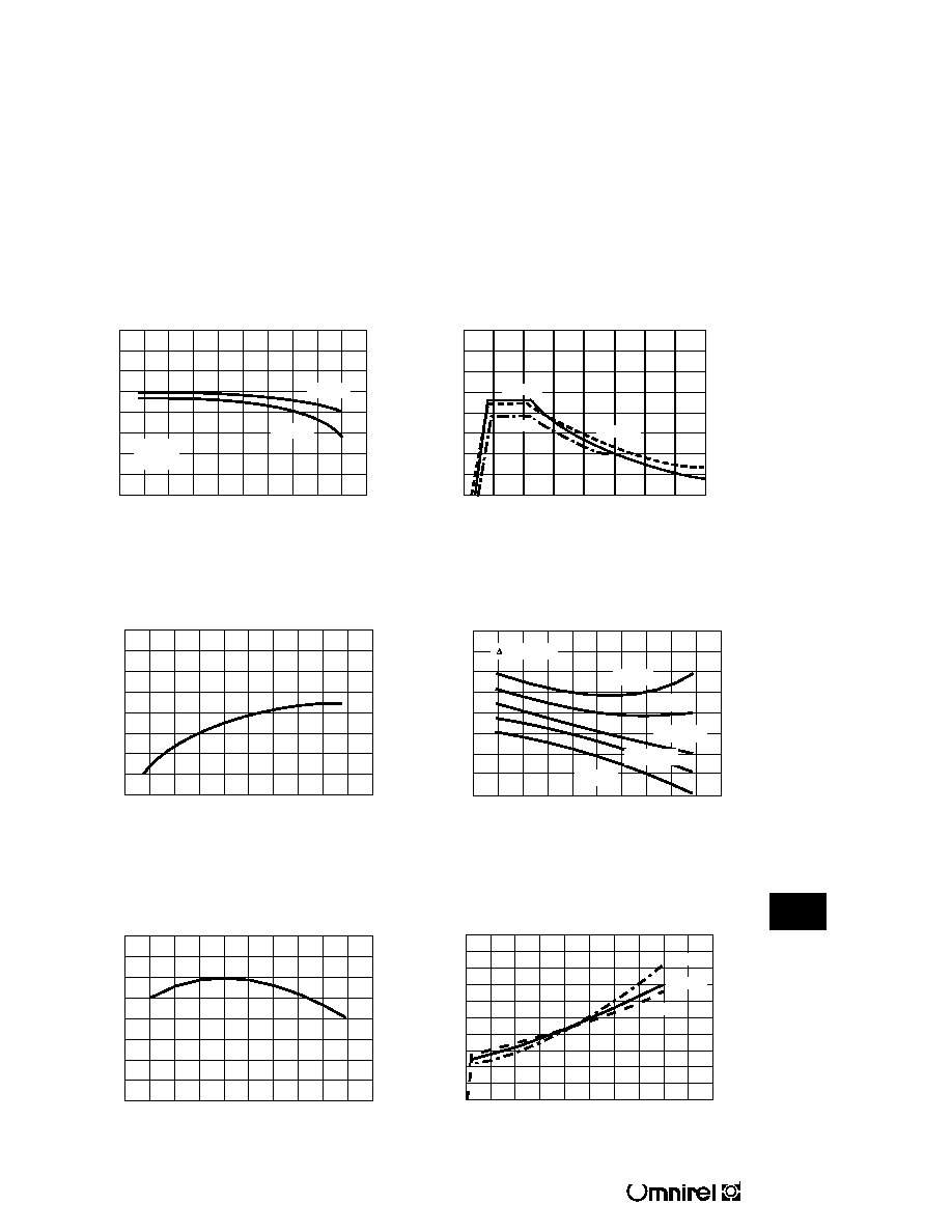
TYPICAL PERFORMANCE CHARACTERISTICS
0.4
0.2
0
-0.2
-0.4
-0.6
-0.8
-1.0
-75
-50
-25
0
25
LOAD REGULATION
T
J
, JUNCTION TEMPERATURE (∞C)
V
O
, OUTPUT VOLTAGE CHANGE (%)
50
75
100
125
150
V
I
= 15V
V
O
= 10V
I
L
= 1.5A
I
L
= 0.5A
4
3
2
1
0
0
10
20
CURRENT LIMIT
V
I
- V
O
, INPUT - OUTPUT VOLTAGE DIFFERENTIAL (V
dc
)
I
O
, OUTPUT CURRENT (A)
30
40
T
J
= -55∞C
T
J
= 25∞C
T
J
= 150∞C
70
65
60
55
50
45
40
35
-75
-50
-25
0
25
ADJUSTMENT PIN CURRENT
T
J
, JUNCTION TEMPERATURE (∞C)
I
Adj
, ADJUSTMENT PIN CURRENT (µA)
50
75
100
125
150
3.0
2.5
2.0
1.5
1.0
-75
-50
-25
0
25
DROPOUT VOLTAGE
T
J
, JUNCTION TEMPERATURE (∞C)
V
I
- V
O,
INPUT-OUTPUT VOLTAGE
DIFFERENTIAL (V
dc
)
50
75
100
125
150
I
L
= 1.5A
I
L
= 1.0A
I
L
= 200mA
I
L
= 20mA
I
L
= 500mA
V
O
= 100mV
1.260
1.250
1.240
1.230
1.220
-75
-50
-25
0
25
TEMPERATURE STABILITY
T
J
, JUNCTION TEMPERATURE (∞C)
V
ref
, REFERENCE VOLTAGE (V)
50
75
100
125
150
5.0
4.5
4.0
3.5
3.0
2.5
2.0
1.5
1.0
0.5
0
0
10
20
MINIMUM OPERATING CURRENT
V
I
- V
O
, INPUT - OUTPUT VOLTAGE DIFFERENTIAL (V
dc
)
I
B
, QUIESCENT CURRENT (mA)
30
40
T
J
= -55∞C
T
J
= 25∞C
T
J
= 150∞C

3.3
205 Crawford Street, Leominster, MA 01453 USA (508) 534-5776 FAX (508) 537-4246
OM7602ST
TYPICAL APPLICATIONS
+25V
V
IN
Adjust
OM7602ST
V
OUT
R1
V
O
I
O
1.25
D
IN
IN4001
D
IN
IN4001
100
R2
V
SS
2N5640
* To provide current limiting of IO to
the system ground, the source of
the FET must be tied to a negative
voltage below -1.25 V.
V
ref
V
ref
R2 R1 =
I
DSS
I
Omax
+ I
DSS
V
O
< BV
DSS
+ 1.25 V + V
SS
I
Lmin
≠ I
DSS
< I
O
< 1.5 A
As shown 0 < I
O
< 1 A
ADJUSTABLE CURRENT LIMITER
D1
V
IN
V
O
OM7602ST
1N4002
1.0µF
MPS2222
TTL
Control
1K
720
Adjust
120
Minimum
V
OUT
= 1.25 V
D1
protects the device during an input short circuit.
5V ELECTRONIC SHUT DOWN REGULATOR
OM7602ST
Adjust
R2
MPS2907
50 K
240
IN4001
+
10 µF
V
IN
V
OU
Adjust
R1
I
OUT
I
Adj
OM7602ST
SLOW TURN-ON REGULATOR
CURRENT REGULATOR
1
2
3
Tab
ISOLATED
NON-ISOLATED
Front View
Front View
Pin 1: Adjust
Pin 1: Adjust
Pin 2: Output
Pin 2: Output
Pin 3: Input
Pin 3: Input
Tab:
Isolated
Tab:
Output
PIN CONNECTION
.430
.410
.200
.190
.038 MAX.
.005
.120 TYP.
.537
.527
.665
.645
.420
.410
.150
.140
.750
.500
.100 TYP.
.035
.025
.045
.035
MECHANICAL OUTLINE
NOTES
∑ Case is metal/hermetically sealed
∑ Isolated Tab
+
(V
REF
) + I
Adj
1.25 V
I
OUT
=
@
R1
R1
10mA I
OUT
1.5 A