Document Outline
- Features
- Description
- ORCA Foundry Development System Overview
- Architecture
- Programmable Logic Cells
- Programmable Input/Output Cells
- Interquad Routing
- Programmable Corner Cells
- Clock Distribution Network
- FPGA States of Operation
- Configuration Data Format
- Bit Stream Error Checking
- FPGA Configuration Modes
- Special Function Blocks
- ORCA Timing Characteristics
- Estimating Power Dissipation
- Pin Information
- Package Thermal Characteristics
- Package Coplanarity
- Package Parasitics
- Absolute Maximum Ratings
- Recommended Operating Conditions
- Electrical Characteristics
- Timing Characteristics
- Measurement Conditions
- Output Buffer Characteristics
- Package Outline Drawings
- Ordering Information
- Terms and Definitions
- 84-Pin PLCC
- 100-Pin TQFP
- 144-Pin TQFP
- 160-Pin QFP
- 208-Pin SQFP
- 208-Pin SQFP2
- 240-Pin SQFP
- 240-Pin SQFP2
- 256-Pin PBGA
- 304-Pin SQFP
- 304-Pin SQFP2
- 352-Pin PBGA
- 432-Pin EBGA
- Index
- Notes
- List of Tables
- Table 1 . ORCA Series 2 FPGAs
- Table 2 . ORCA Series 2 System Performance
- Table 3 . Look-Up Table Operating Modes
- Table 4 . Configuration RAM Controlled Latch/ Flip-Flop Operation
- Table 5 . Inter-PLC Routing Resources
- Table 6 . Input/Output Cell Options
- Table 7 . Configuration Frame Size
- Table 8 . Configuration Data Frames
- Table 9 . Configuration Frame Format and Contents
- Table 10 . Configuration Modes
- Table 11 . Readback Options
- Table 12 . Boundary-Scan Instructions
- Table 13 . TAP Controller Input/Outputs
- Table 14 A. Derating for Commercial Devices (OR2CxxA)
- Table 14 B. Derating for Industrial Devices (OR2CxxA)
- Table 15 A. Derating for Commercial/Industrial Devices (OR2TxxA)
- Table 15 B. Derating for Commercial/Industrial Devices (OR2TxxB)
- Table 16 . dc Power for 5 V Tolerant I/Os for OR2TxxA deviced
- Table 17 . Pin Descriptions (continued)
- Table 18 A. ORCA OR2CxxA and OR2TxxB Series FPGA I/Os Summary
- Table 18 B. ORCA OR2TxxA Series FPGA I/Os Summary
- Table 18 C. Series 3 ExpressCLK Pins
- Table 19 . OR2C/2T04A, OR2C/2T06A, OR2C/2T08A, OR2C/2T10A, OR2C/2T12A, and OR2C/2T15A 84-Pin PLCC...
- Table 20. OR2C/2T04A and OR2C/2T06A 100-Pin TQFP Pinout (continued)
- Table 21. OR2C/2T04A and OR2C/2T06A 144-Pin TQFP Pinout (continued)
- Table 22. OR2C/2T04A, OR2C/2T06A, OR2C/2T08A, and OR2C/2T10A 160-Pin QFP Pinout (continued)
- Table 23. OR2C/2T04A, OR2C/2T06A, OR2C/2T08A, OR2C/2T10A, OR2C/2T12A, OR2C/2T15A/B, OR2C/2T26A, a...
- Table 24. �OR2C/2T06A, OR2C/2T08A, OR2C/2T10A, OR2C/2T12A, OR2C/2T15A/B, OR2C/2T26A, and OR2C/2T4...
- Table 25 . OR2C/2T06A, OR2C/2T08A, OR2C/2T10A, OR2C/2T12A, and OR2C/2T15A/B 256-Pin PBGA Pinout (...
- Table 26. �OR2C12A, OR2C15A, OR2C26A, and OR2C40A 304-Pin SQFP/SQFP2 Pinout (continued)
- Table 27. OR2C/2T10A, OR2C/2T12A, OR2C/2T15A/B, OR2C/2T26A, and OR2T40A/B 352-Pin PBGA Pinout (co...
- Table 28. �OR2C/2T15A, OR2C/2T26A, and OR2C/2T40A/B 432-Pin EBGA Pinout (continued)
- Table 29 . Series 2 Plastic Package Thermal Guidelines
- Table 30 . Series 2 Package Parasitics
- Table 31 A. OR2CxxA and OR2TxxA Electrical Characteristics
- Table 31 B. OR2TxxB Electrical Characteristics
- Table 32 A. OR2CxxA and OR2TxxA Combinatorial PFU Timing Characteristics �
- Table 32 B. OR2TxxB Combinatorial PFU Timing Characteristics �
- Table 33 A. OR2CxxA and OR2TxxA Sequential PFU Timing Characteristics�
- Table 33 B. OR2TxxB Sequential PFU Timing Characteristics�
- Table 34 A. OR2CxxA and OR2TxxA Ripple Mode PFU Timing Characteristics
- Table 34 B. OR2TxxB Ripple Mode PFU Timing Characteristics
- Table 35 A. OR2CxxA and OR2TxxA Asynchronous Memory Read Characteristics (MA/MB Modes)
- Table 35 B. OR2TxxB Asynchronous Memory Read Characteristics (MA/MB Modes)
- Table 36 A. OR2CxxA and OR2TxxA Asynchronous Memory Write Characteristics (MA/MB Modes)
- Table 36 B. OR2TxxB Asynchronous Memory Write Characteristics (MA/MB Modes)
- Table 37 A. OR2CxxA and OR2TxxA Asynchronous Memory Read During Write Operation (MA/MB Modes)
- Table 37 B. OR2TxxB Asynchronous Memory Read During Write Operation (MA/MB Modes)
- Table 38 A. OR2CxxA and OR2TxxA Asynchronous Memory Read During Write, Clocking Data into Latch/ ...
- Table 38 B. OR2TxxB Asynchronous Memory Read During Write, Clocking Data into Latch/Flip-Flop (MA...
- Table 39 A. OR2CxxA and OR2TxxA Synchronous Memory Write Characteristics (SSPM and SDPM Modes)
- Table 39. B OR2TxxB Synchronous Memory Write Characteristics (SSPM and SDPM Modes) (continued)
- Table 40 A. OR2CxxA and OR2TxxA Synchronous Memory Read Characteristics (SSPM and SDPM Modes)
- Table 40 B. OR2TxxB Synchronous Memory Read Characteristics (SSPM and SDPM Modes)
- Table 41 A. OR2CxxA and OR2TxxA PFU Output MUX, PLC BIDI, and Direct Routing Timing Characteristics
- Table 41 B. OR2TxxB PFU Output MUX, PLC BIDI, and Direct Routing Timing Characteristics
- Table 42 A. OR2CxxA and OR2TxxA Internal Clock Delay
- Table 42 B. OR2TxxB Internal Clock Delay
- Table 43 A. OR2CxxA and OR2TxxA OR2CxxA/OR2TxxA Global Clock to Output Delay (Pin-to-Pin)ÑOutput ...
- Table 43 B. OR2TxxB Global Clock to Output Delay (Pin-to-Pin)ÑOutput on Same Side of the Device a...
- Table 44 A. OR2CxxA/OR2TxxA Global Clock to Output Delay (Pin-to-Pin)ÑOutput Not on Same Side of ...
- Table 44 B. OR2TxxB Global Clock to Output Delay (Pin-to-Pin)ÑOutput Not on Same Side of the Devi...
- Table 45 A. OR2CxxA/OR2TxxA Global Input to Clock Setup/Hold Time (Pin-to-Pin)
- Table 45 B. OR2TxxB Global Input to Clock Setup/Hold Time (Pin-to-Pin)�
- Table 46 A. OR2CxxA/OR2TxxA Programmable I/O Cell Timing Characteristics
- Table 46 B. OR2TxxB Programmable I/O Cell Timing Characteristics
- Table 47 . Series 2 General Configuration Mode Timing Characteristics (continued)
- Table 48 . Series 2 Master Serial Configuration Mode Timing Characteristics
- Table 49 . Series 2 Master Parallel Configuration Mode Timing Characteristics
- Table 50 . Series 2 Asynchronous Peripheral Configuration Mode Timing Characteristics
- Table 51 A. OR2CxxA/OR2TxxA Synchronous Peripheral Configuration Mode Timing Characteristics
- Table 51 B. OR2TxxB Synchronous Peripheral Configuration Mode Timing Characteristics
- Table 52 A. OR2CxxA/OR2TxxA Slave Serial Configuration Mode Timing Characteristics
- Table 52 B. OR2TxxB Slave Serial Configuration Mode Timing Characteristics
- Table 53 A. OR2CxxA/OR2TxxA Slave Parallel Configuration Mode Timing Characteristics
- Table 53 B. OR2TxxB Slave Parallel Configuration Mode Timing Characteristics
- Table 54 . Series 2 Readback Timing Characteristics
- Table 55 . Series 2 Boundary-Scan Timing Characteristics
- Table 56 . FPGA Voltage Options
- Table 57 . FPGA Temperature Options
- Table 58 . FPGA Package Options
- Table 59 . ORCA OR2CxxA/OR2TxxA Series Package Matrix
- Table 60 . ORCA OR2TxxB Series Package Matrix
- List of Figures
- Figure 1 . Series 2 Array
- Figure 2 . PFU Ports
- Figure 3 . Simplified PFU Diagram
- Figure 4 . F4 ModeÑFour Functions of Four- Input Variables
- Figure 5 . F5 ModeÑTwo Functions of Five-Input Variables
- Figure 6 . F5M ModeÑMultiplexed Function of Two Independent Five-Input Variable Functions
- Figure 7 . F5X ModeÑExclusive OR Function of Two Independent Five-Input Variable Functions
- Figure 8 . F5M ModeÑOne Six-Input Variable Function
- Figure 9 . Ripple Mode
- Figure 10 . Counter Submode with Flip-Flops
- Figure 11 . Multiplier Submode
- Figure 12 . MA/MB ModeÑ16 x 4 RAM
- Figure 13 . MA/F5 ModeÑ16 x 2 Memory and One Function of Five Input Variables
- Figure 14 . SSPM ModeÑ16 x 4 Synchronous Single-Port Memory
- Figure 15 . SSPM with Read/Write per Clock Cycle
- Figure 16 . Synchronous RAM with Write-Port Enable (WPE)
- Figure 17 . SDPM ModeÑ16 x 2 Synchronous Dual-Port Memory
- Figure 18 . Latch/FF Set/Reset Configurations
- Figure 19 . Configurable Interconnect Point
- Figure 20 . 3-Statable Bidirectional Buffers
- Figure 21 . Single PLC View of Inter-PLC Lines
- Figure 22 . Multiple PLC View of Inter-PLC Routing
- Figure 23 . PLC Architecture
- Figure 24 . Simplified Diagrams
- Figure 25 . Simplified PIC Routing Diagram
- Figure 26 . PIC Architecture
- Figure 27 . PIC Detail
- Figure 28 . Interquad Routing
- Figure 29 . hIQ Block Detail
- Figure 30 . Subquad Blocks and Subquad Routing
- Figure 31 . Horizontal Subquad Routing Connectivity
- Figure 32 . Horizontal Subquad Routing Connectivity (Half Quad)
- Figure 33 . Top (TMID) Routing
- Figure 34 . Primary Clock Distribution
- Figure 35 . Secondary Clock Distribution
- Figure 36 . FPGA States of Operation
- Figure 37 . Initialization/Configuration/Start-Up Waveforms
- Figure 38 . Start-Up Waveforms
- Figure 39 . Serial Configuration Data Format
- Figure 40 . Master Parallel Configuration Schematic
- Figure 41 . Master Serial Configuration Schematic
- Figure 42 . Asynchronous Peripheral Configuration Schematic
- Figure 43 . Synchronous Peripheral Configuration Schematic
- Figure 44 . Slave Serial Configuration Schematic
- Figure 45 . Slave Parallel Configuration Schematic
- Figure 46 . Daisy-Chain Configuration Schematic
- Figure 47 . Printed-Circuit Board with Boundary- Scan Circuitry
- Figure 48 . Boundary-Scan Interface
- Figure 49 . ORCA Series Boundary-Scan Circuitry Functional Diagram
- Figure 50 . TAP Controller State Transition Diagram
- Figure 51 . Boundary-Scan Cell
- Figure 52 . Instruction Register Scan Timing Diagram
- Figure 53 . Package Parasitics
- Figure 54 . Combinatorial PFU Timing
- Figure 55 . Read OperationÑFlip-Flop Bypass
- Figure 56 . Read OperationÑLUT Memory Loading Flip-Flops
- Figure 57 . Write Operation
- Figure 58 . Read During Write
- Figure 59 . Read During WriteÑClocking Data into Flip-Flop
- Figure 60 . Synchronous Memory Write Characteristics
- Figure 61 . Synchronous Memory Read Cycle
- Figure 62 . Global Clock to Output Delay
- Figure 63 . Global Clock to Output Delay
- Figure 64 . Global Input to Clock Setup/Hold Time
- Figure 65 . General Configuration Mode Timing Diagram
- Figure 66 . Master Serial Configuration Mode Timing Diagram
- Figure 67 . Master Parallel Configuration Mode Timing Diagram
- Figure 68 . Asynchronous Peripheral Configuration Mode Timing Diagram
- Figure 69 . Synchronous Peripheral Configuration Mode Timing Diagram
- Figure 70 . Slave Serial Configuration Mode Timing Diagram
- Figure 71 . Slave Parallel Configuration Mode Timing Diagram
- Figure 72 . Readback Timing Diagram
- Figure 73 . Boundary-Scan Timing Diagram
- Figure 74 . ac Test Loads
- Figure 75 . Output Buffer Delays
- Figure 76 . Input Buffer Delays
- Figure 77 . Sinklim (TJ = 25 ∞C, VDD = 5.0 V)
- Figure 78 . Slewlim (TJ = 25 ∞C, VDD = 5.0 V)
- Figure 79 . Fast (TJ = 25 ∞C, VDD = 5.0 V)
- Figure 80 . Sinklim (TJ = 125 ∞C, VDD = 4.5 V)
- Figure 81 . Slewlim (TJ = 125 ∞C, VDD = 4.5 V)
- Figure 82 . Fast (TJ = 125 ∞C, VDD = 4.5 V)
- Figure 83 . Sinklim (TJ = 25 ∞C, VDD = 3.3 V)
- Figure 84 . Slewlim (TJ = 25 ∞C, VDD = 3.3 V)
- Figure 85 . Fast (TJ = 25 ∞C, VDD = 3.3 V)
- Figure 86 . Sinklim (TJ = 125 ∞C, VDD = 3.0 V)
- Figure 87 . Slewlim (TJ = 125 ∞C, VDD = 3.0 V)
- Figure 88 . Fast (TJ = 125 ∞C, VDD = 3.0 V)
- Figure 89 . Sinklim (TJ = 25 ∞C, VDD = 3.3 V)
- Figure 90 . Slewlim (TJ = 25 ∞C, VDD = 3.3 V)
- Figure 91 . Fast (TJ = 25 ∞C, VDD = 3.3 V)
- Figure 92 . Sinklim (TJ = 125 ∞C, VDD = 3.0 V)
- Figure 93 . Slewlim (TJ = 125 ∞C, VDD = 3.0 V)
- Figure 94 . Fast (TJ = 125 ∞C, VDD = 3.0 V)
ORCA
Æ
Series 2
Field-Programmable Gate Arrays
Data Sheet
June 1999
Features
s
High-performance, cost-effective, low-power
0.35 µm CMOS technology (OR2CxxA), 0.3 µm CMOS
technology (OR2TxxA), and 0.25 µm CMOS technology
(OR2TxxB), (four-input look-up table (LUT) delay less
than 1.0 ns with -8 speed grade)
s
High density (up to 43,200 usable, logic-only gates; or
99,400 gates including RAM)
s
Up to 480 user I/Os (OR2TxxA and OR2TxxB I/Os are
5 V tolerant to allow interconnection to both 3.3 V and
5 V devices, selectable on a per-pin basis)
s
Four 16-bit look-up tables and four latches/flip-flops per
PFU, nibble-oriented for implementing 4-, 8-, 16-, and/or
32-bit (or wider) bus structures
s
Eight 3-state buffers per PFU for on-chip bus structures
s
Fast, on-chip user SRAM has features to simplify RAM
design and increase RAM speed:
-- Asynchronous single port: 64 bits/PFU
-- Synchronous single port: 64 bits/PFU
-- Synchronous dual port: 32 bits/PFU
s
Improved ability to combine PFUs to create larger RAM
structures using write-port enable and 3-state buffers
s
Fast, dense multipliers can be created with the multiplier
mode (4 x 1 multiplier/PFU):
-- 8 x 8 multiplier requires only 16 PFUs
-- 30% increase in speed
s
Flip-flop/latch options to allow programmable priority of
synchronous set/reset vs. clock enable
s
Enhanced cascadable nibble-wide data path
capabilities for adders, subtractors, counters, multipliers,
and comparators including internal fast-carry operation
s
Innovative, abundant, and hierarchical nibble-
oriented routing resources that allow automatic use of
internal gates for all device densities without sacrificing
performance
s
Upward bit stream compatible with the
ORCA ATT2Cxx/
ATT2Txx series of devices
s
Pinout-compatible with new
ORCA Series 3 FPGAs
s
TTL or CMOS input levels programmable per pin for the
OR2CxxA (5 V) devices
s
Individually programmable drive capability:
12 mA sink/6 mA source or 6 mA sink/3 mA source
s
Built-in boundary scan (
IEEE*1149.1 JTAG) and
3-state all I/O pins, (TS_ALL) testability functions
s
Multiple configuration options, including simple, low pin-
count serial ROMs, and peripheral or JTAG modes for in-
system programming (ISP)
s
Full PCI bus compliance for all devices
s
Supported by industry-standard CAE tools for design
entry, synthesis, and simulation with
ORCA Foundry
Development System support (for back-end implementa-
tion)
s
New, added features (OR2TxxB) have:
-- More I/O per package than the OR2TxxA family
-- No dedicated 5 V supply (V
DD
5)
-- Faster configuration speed (40 MHz)
-- Pin selectable I/O clamping diodes provide 5V or 3.3V
PCI compliance and 5V tolerance
-- Full PCI bus compliance in both 5V and 3.3V PCI sys-
tems
*
IEEE
is a registered trademark of The Institute of Electrical and
Electronics Engineers, Inc.
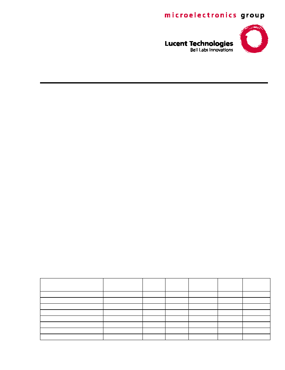
Table 1
. ORCA
Series 2 FPGAs
* The first number in the usable gates column assumes 48 gates per PFU (12 gates per four-input LUT/FF pair) for logic-only designs. The
second number assumes 30% of a design is RAM. PFUs used as RAM are counted at four gates per bit, with each PFU capable of
implementing a 16 x 4 RAM (or 256 gates) per PFU.
Device
Usable
Gates*
# LUTs
Registers
Max User
RAM Bits
User
I/Os
Array Size
OR2C04A/OR2T04A
4,800--11,000
400
400
6,400
160
10 x 10
OR2C06A/OR2T06A
6,900--15,900
576
576
9,216
192
12 x 12
OR2C08A/OR2T08A
9,400--21,600
784
724
12,544
224
14 x 14
OR2C10A/OR2T10A
12,300--28,300
1024
1024
16,384
256
16 x 16
OR2C12A/OR2T12A
15,600--35,800
1296
1296
20,736
288
18 x 18
OR2C15A/OR2T15A/OR2T15B
19,200--44,200
1600
1600
25,600
320
20 x 20
OR2C26A/OR2T26A
27,600--63,600
2304
2304
36,864
384
24 x 24
OR2C40A/OR2T40A/OR2T40B
43,200--99,400
3600
3600
57,600
480
30 x 30

Data Sheet
ORCA Series 2 FPGAs
June 1999
2
Lucent Technologies Inc.
Table of Contents
Contents
Page
Contents
Page
Features ...................................................................... 1
Description................................................................... 3
ORCA
Foundry Development System Overview......... 5
Architecture ................................................................. 5
Programmable Logic Cells .......................................... 5
Programmable Function Unit ................................... 5
Look-Up Table Operating Modes ............................ 7
Latches/Flip-Flops ................................................. 15
PLC Routing Resources ........................................ 17
PLC Architectural Description................................ 22
Programmable Input/Output Cells ............................. 25
Inputs ..................................................................... 25
Outputs .................................................................. 26
5 V Tolerant I/O (OR2TxxB) .................................. 27
PCI Compliant I/O.................................................. 27
PIC Routing Resources ......................................... 28
PIC Architectural Description................................. 29
PLC-PIC Routing Resources ................................. 30
Interquad Routing ...................................................... 32
Subquad Routing (OR2C40A/OR2T40A Only)...... 34
PIC Interquad (MID) Routing ................................. 36
Programmable Corner Cells ...................................... 37
Programmable Routing.......................................... 37
Special-Purpose Functions.................................... 37
Clock Distribution Network ........................................ 37
Primary Clock ........................................................ 37
Secondary Clock ................................................... 38
Selecting Clock Input Pins ..................................... 39
FPGA States of Operation......................................... 40
Initialization ............................................................ 40
Configuration ......................................................... 41
Start-Up ................................................................. 42
Reconfiguration ..................................................... 42
Partial Reconfiguration .......................................... 43
Other Configuration Options .................................. 43
Configuration Data Format ........................................ 43
Using
ORCA
Foundry to Generate
Configuration RAM Data..................................... 44
Configuration Data Frame ..................................... 44
Bit Stream Error Checking......................................... 47
FPGA Configuration Modes....................................... 47
Master Parallel Mode............................................. 47
Master Serial Mode ............................................... 48
Asynchronous Peripheral Mode ............................ 49
Synchronous Peripheral Mode .............................. 49
Slave Serial Mode ................................................. 50
Slave Parallel Mode............................................... 50
Daisy Chain ........................................................... 51
Special Function Blocks ............................................ 52
Single Function Blocks .......................................... 52
Boundary Scan ...................................................... 54
Boundary-Scan Instructions...................................55
ORCA
Boundary-Scan Circuitry ............................56
ORCA
Timing Characteristics....................................60
Estimating Power Dissipation ....................................61
OR2CxxA...............................................................61
OR2TxxA ...............................................................63
OR2T15B and OR2T40B .......................................65
Pin Information ..........................................................66
Pin Descriptions.....................................................66
Package Compatibility ...........................................68
Compatibility with Series 3 FPGAs ........................70
Package Thermal Characteristics............................126
QJA ......................................................................126
yJC.......................................................................126
QJC......................................................................126
QJB......................................................................126
Package Coplanarity ...............................................127
Package Parasitics ..................................................127
Absolute Maximum Ratings .....................................129
Recommended Operating Conditions......................129
Electrical Characteristics .........................................130
Timing Characteristics .............................................132
Series 2................................................................160
Measurement Conditions.........................................169
Output Buffer Characteristics...................................170
OR2CxxA.............................................................170
OR2TxxA .............................................................171
OR2TxxB .............................................................172
Package Outline Drawings ......................................173
Terms and Definitions ..........................................173
84-Pin PLCC........................................................174
100-Pin TQFP ......................................................175
144-Pin TQFP ......................................................176
160-Pin QFP ........................................................177
208-Pin SQFP......................................................178
208-Pin SQFP2....................................................179
240-Pin SQFP......................................................180
240-Pin SQFP2....................................................181
256-Pin PBGA .....................................................182
304-Pin SQFP......................................................183
304-Pin SQFP2....................................................184
352-Pin PBGA .....................................................185
432-Pin EBGA .....................................................186
Ordering Information................................................187
Index ........................................................................189

Data Sheet
June 1999
ORCA Series 2 FPGAs
Lucent Technologies Inc.
3
Description
The
ORCA
Series 2 series of SRAM-based FPGAs are
an enhanced version of the ATT2C/2T architecture.
The latest
ORCA
series includes patented architectural
enhancements that make functions faster and easier to
design while conserving the use of PLCs and routing
resources.
The Series 2 devices can be used as drop-in replace-
ments for the ATT2Cxx/ATT2Txx series, respectively,
and they are also bit stream compatible with each
other. The usable gate counts associated with each
series are provided in Table 1. Both series are offered
in a variety of packages, speed grades, and tempera-
ture ranges.
The
ORCA
series FPGA consists of two basic ele-
ments: programmable logic cells (PLCs) and program-
mable input/output cells (PICs). An array of PLCs is
surrounded by PICs as shown in Figure 1. Each PLC
contains a programmable function unit (PFU). The
PLCs and PICs also contain routing resources and
configuration RAM. All logic is done in the PFU. Each
PFU contains four 16-bit look-up tables (LUTs) and four
latches/flip-flops (FFs).
The PLC architecture provides a balanced mix of logic
and routing that allows a higher utilized gate/PFU than
alternative architectures. The routing resources carry
logic signals between PFUs and I/O pads. The routing
in the PLC is symmetrical about the horizontal and ver-
tical axes. This improves routability by allowing a bus of
signals to be routed into the PLC from any direction.
Some examples of the resources required and the per-
formance that can be achieved using these devices are
represented in Table 2.
Table 2
. ORCA
Series 2 System Performance
1. Implemented using 4 x 1 multiplier mode (unpipelined), register-to-register, two 8-bit inputs, one 16-bit output.
2. Implemented using two 16 x 12 ROMs and one 12-bit adder, one 8-bit input, one fixed operand, one 16-bit output.
3. Implemented using 4 x 1 multiplier mode (fully pipelined), two 8-bit inputs, one 16-bit output (28 of 44 PFUs contain only pipelining registers).
4. Implemented using 16 x 4 synchronous single-port RAM mode allowing both read and write per clock cycle, including write/read address
multiplexer.
5. Implemented using 16 x 4 synchronous single-port RAM mode allowing either read or write per clock cycle, including write/read address mul-
tiplexer.
6. Implemented using 16 x 2 synchronous dual-port RAM mode.
7. OR2TxxB available only in -7 and -8 speeds only.
8. Speed grades of -5, -6, and -7 are for OR2TxxA devices only.
Function
#
PFUs
Speed Grade
Unit
-2A
-3A
-4A
-5A
-6A
-7A
-7B
-8B
16-bit loadable up/down
counter
4
51.0
66.7
87.0
104.2
129.9
144.9
131.6
149.3
MHz
16-bit accumulator
4
51.0
66.7
87.0
104.2
129.9
144.9
131.6
149.3
MHz
8 x 8 parallel multiplier:
-- Multiplier mode, unpipelined
1
-- ROM mode, unpipelined
2
-- Multiplier mode, pipelined
3
22
9
44
14.2
41.5
50.5
19.3
55.6
69.0
25.1
71.9
82.0
31.0
87.7
103.1
36.0
107.5
125.0
40.3
122.0
142.9
37.7
103.1
123.5
44.8
120.5
142.9
MHz
MHz
MHz
32 x 16 RAM:
-- Single port (read and write/
cycle)
4
-- Single port
5
-- Dual port
6
9
9
16
21.8
38.2
38.2
28.6
52.6
52.6
36.2
69.0
83.3
53.8
92.6
92.6
53.8
92.6
92.6
62.5
96.2
96.2
57.5
97.7
97.7
69.4
112.4
112.4
MHz
MHz
MHz
36-bit parity check (internal)
4
13.9
11.0
9.1
7.4
5.6
5.2
6.1
5.1
ns
32-bit address decode
(internal)
3.25
12.3
9.5
7.5
6.1
4.6
4.3
4.8
4.0
ns

Data Sheet
ORCA Series 2 FPGAs
June 1999
4
Lucent Technologies Inc.
Description
(continued)
The FPGA's functionality is determined by internal configuration RAM. The FPGA's internal initialization/configura-
tion circuitry loads the configuration data at powerup or under system control. The RAM is loaded by using one of
several configuration modes. The configuration data resides externally in an EEPROM, EPROM, or ROM on the
circuit board, or any other storage media. Serial ROMs provide a simple, low pin count method for configuring
FPGAs, while the peripheral and JTAG configuration modes allow for easy, in-system programming (ISP).
5-6779(F)
Figure 1. Series 2 Array
PL
9
P
L8
P
L
7
P
L6
P
L
5
P
L4
P
L
3
P
L2
P
L
1
PL
13
PL
12
PL
11
PR
1
2
PR
11
PR
9
PR
8
PR
7
PR
6
PR
5
PR
4
PR
3
PR
2
PR
1
P
R
13
PR
18
PR
17
PR
1
6
PR
1
5
PR
1
4
RMI
D
PR
1
0
PT1
PT2
PT3
PT4
PT5
PT6
PT7
PT8
PT9
PT11
PT12
R1C1
R1C2
R1C3
R1C4
R1C5
R1C6
R1C7
R1C8
R1C9
R1C10
R1C18
R1C17
R1C16
R1C15
R1C14
R1C13
R1C12
R1C11
PT13
PT14
PT15
PT16
PT17
PT18
PB1
PB2
PB3
PB4
PB5
PB6
PB7
PB8
PB9
PB10
PB11
PB12
PL
18
PL
17
PL
16
PL
15
PL
14
PB13
PB14
PB15
PB16
PB17
PB18
P
L10
BMID
PT10
vIQ
R2C1
R2C2
R2C3
R2C4
R2C5
R2C6
R2C7
R2C8
R2C9
R2C10
R3C1
R3C2
R3C3
R3C4
R3C5
R3C6
R3C7
R3C8
R3C9
R3C10
R4C1
R4C2
R4C3
R4C4
R4C5
R4C6
R4C7
R4C8
R4C9
R4C10
R5C1
R5C2
R5C3
R5C4
R5C5
R5C6
R5C7
R5C8
R5C9
R5C10
R6C1
R6C2
R6C3
R6C4
R6C5
R6C6
R6C7
R6C8
R6C9
R6C10
R7C1
R7C2
R7C3
R7C4
R7C5
R7C6
R7C7
R7C8
R7C9
R7C10
R8C1
R8C2
R8C3
R8C4
R8C5
R8C6
R8C7
R8C8
R8C9
R8C10
R9C1
R9C2
R9C3
R9C4
R9C5
R9C6
R9C7
R9C8
R9C9
R9C10
R10C1 R10C2 R10C3
R10C4 R10C5 R10C6
R10C7 R10C8 R10C9
R10C10
R2C18
R2C17
R2C16
R2C15
R2C14
R2C13
R2C12
R2C11
R3C18
R3C17
R13C16
R3C15
R3C14
R3C13
R3C12
R3C11
R4C18
R4C17
R4C16
R4C15
R4C14
R4C13
R4C12
R4C11
R5C18
R5C17
R5C16
R5C15
R5C14
R5C13
R5C12
R5C11
R6C18
R6C17
R6C16
R6C15
R6C14
R6C13
R6C12
R6C11
R7C18
R7C17
R7C16
R7C15
R7C14
R7C13
R7C12
R7C11
R8C18
R8C17
R8C16
R8C15
R8C14
R8C13
R8C12
R8C11
R9C18
R9C17
R9C16
R9C15
R9C14
R9C13
R9C12
R9C11
R10C18
R10C17
R10C16
R10C15
R10C14
R10C13
R10C12
R10C11
R18C18
R18C17
R18C16
R18C15
R18C14
R18C13
R18C12
R18C11
R17C18
R17C17
R17C16
R17C15
R17C14
R17C13
R17C12
R17C11
R16C18
R16C17
R16C16
R16C15
R16C14
R16C13
R16C12
R16C11
R15C18
R15C17
R15C16
R15C15
R15C14
R15C13
R15C12
R15C11
R14C18
R14C17
R14C16
R14C15
R14C14
R14C13
R14C12
R14C11
R13C18
R13C17
R13C16
R13C15
R13C14
R13C13
R13C12
R13C11
R12C18
R12C17
R12C16
R12C15
R12C14
R12C13
R12C12
R12C11
R11C18
R11C17
R11C16
R11C15
R11C14
R11C13
R11C12
R11C11
R18C10
R18C9
R18C8
R18C7
R18C6
R18C5
R18C4
R18C3
R18C2
R18C1
R17C10
R17C9
R17C8
R17C7
R17C6
R17C5
R17C4
R17C3
R17C2
R17C1
R16C10
R16C9
R16C8
R16C7
R16C6
R16C5
R16C4
R16C3
R16C2
R16C1
R15C10
R15C9
R15C8
R15C7
R15C6
R15C5
R15C4
R15C3
R15C2
R15C1
R14C10
R14C9
R14C8
R14C7
R14C6
R14C5
R14C4
R14C3
R14C2
R14C1
R13C10
R13C9
R13C8
R13C7
R13C6
R13C5
R13C4
R13C3
R13C2
R13C1
R12C10
R12C9
R12C8
R12C7
R12C6
R12C5
R12C4
R12C3
R12C2
R12C1
R11C10
R11C9
R11C8
R11C7
R11C6
R11C5
R11C4
R11C3
R11C2
R11C1
hIQ
TMID
LM
ID
Lucent Technologies Inc.
5
Data Sheet
June 1999
ORCA Series 2 FPGAs
ORCA
Foundry
Development System
Overview
The
ORCA
Foundry Development System interfaces to
front-end design entry tools and provides the tools to
produce a configured FPGA. In the design flow, the
user defines the functionality of the FPGA at two
points: at design entry and at the bit stream generation
stage.
Following design entry, the development system's map,
place, and route tools translate the netlist into a routed
FPGA. Its bit stream generator is then used to generate
the configuration data which is loaded into the FPGA's
internal configuration RAM. When using the bit stream
generator, the user selects options that affect the func-
tionality of the FPGA. Combined with the front-end
tools,
ORCA
Foundry produces configuration data that
implements the various logic and routing options dis-
cussed in this data sheet.
Architecture
The
ORCA
Series FPGA is comprised of two basic
elements: PLCs and PICs. Figure 1 shows an array of
programmable logic cells (PLCs) surrounded by pro-
grammable input/output cells (PICs). The Series 2 has
PLCs arranged in an array of 20 rows and 20 columns.
PICs are located on all four sides of the FPGA between
the PLCs and the IC edge.
The location of a PLC is indicated by its row and col-
umn so that a PLC in the second row and third column
is R2C3. PICs are indicated similarly, with PT (top) and
PB (bottom) designating rows and PL (left) and PR
(right) designating columns, followed by a number. The
routing resources and configuration RAM are not
shown, but the interquad routing blocks (hIQ, vIQ)
present in the Series 2 series are shown.
Each PIC contains the necessary I/O buffers to inter-
face to bond pads. The PICs also contain the routing
resources needed to connect signals from the bond
pads to/from PLCs. The PICs do not contain any user-
accessible logic elements, such as flip-flops.
Combinatorial logic is done in look-up tables (LUTs)
located in the PFU. The PFU can be used in different
modes to meet different logic requirements. The LUT's
configurable medium-/large-grain architecture can be
used to implement from one to four combinatorial logic
functions. The flexibility of the LUT to handle wide input
functions, as well as multiple smaller input functions,
maximizes the gate count/PFU.
The LUTs can be programmed to operate in one of
three modes: combinatorial, ripple, or memory. In com-
binatorial mode, the LUTs can realize any four-, five-,
or six-input logic functions. In ripple mode, the high-
speed carry logic is used for arithmetic functions, the
new multiplier function, or the enhanced data path
functions. In memory mode, the LUTs can be used as a
16 x 4 read/write or read-only memory (asynchronous
mode or the new synchronous mode) or a new 16 x 2
dual-port memory.
Programmable Logic Cells
The programmable logic cell (PLC) consists of a pro-
grammable function unit (PFU) and routing resources.
All PLCs in the array are identical. The PFU, which con-
tains four LUTs and four latches/FFs for logic imple-
mentation, is discussed in the next section.
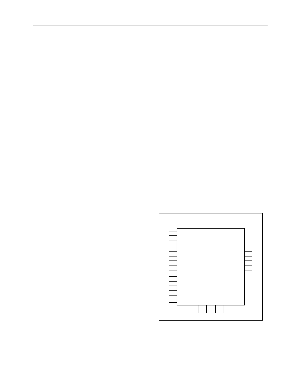
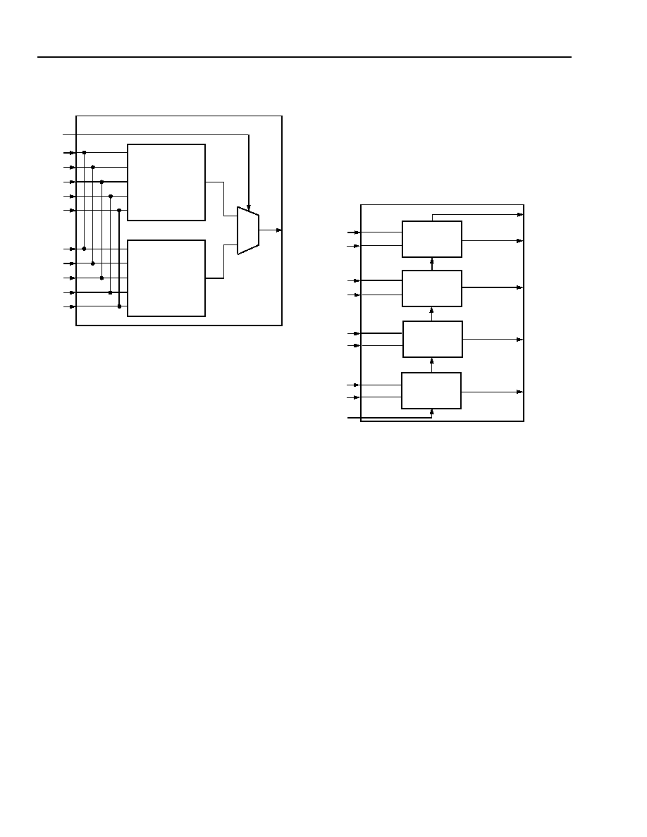
Programmable Function Unit
The PFUs are used for logic. Each PFU has 19 exter-
nal inputs and six outputs and can operate in several
modes. The functionality of the inputs and outputs
depends on the operating mode.
The PFU uses three input data buses (A[4:0], B[4:0],
WD[3:0]), four control inputs (C0, CK, CE, LSR), and a
carry input (CIN); the last is used for fast arithmetic
functions. There is a 5-bit output bus (O[4:0]) and a
carry-out (COUT).
5-2750(F).r3
Figure 2. PFU Ports
PROGRAMMABLE LOGIC CELL (PLC)
WD3
WD2
WD1
WD0
A4
A3
A2
A1
A0
B4
B3
B2
B1
B0
O4
O3
O2
O1
O0
PROGRAMMABLE
FUNCTION UNIT
CE LSR
C0 CK
(ROUTING RESOURCES, CONFIGURATION RAM)
CIN
(PFU)
COUT
Data Sheet
ORCA Series 2 FPGAs
June 1999
6
Lucent Technologies Inc.
Programmable Logic Cells
(continued))
Key: C = controlled by configuration RAM.
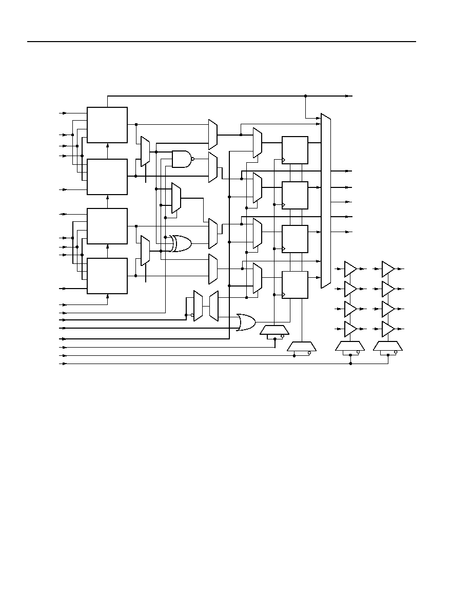
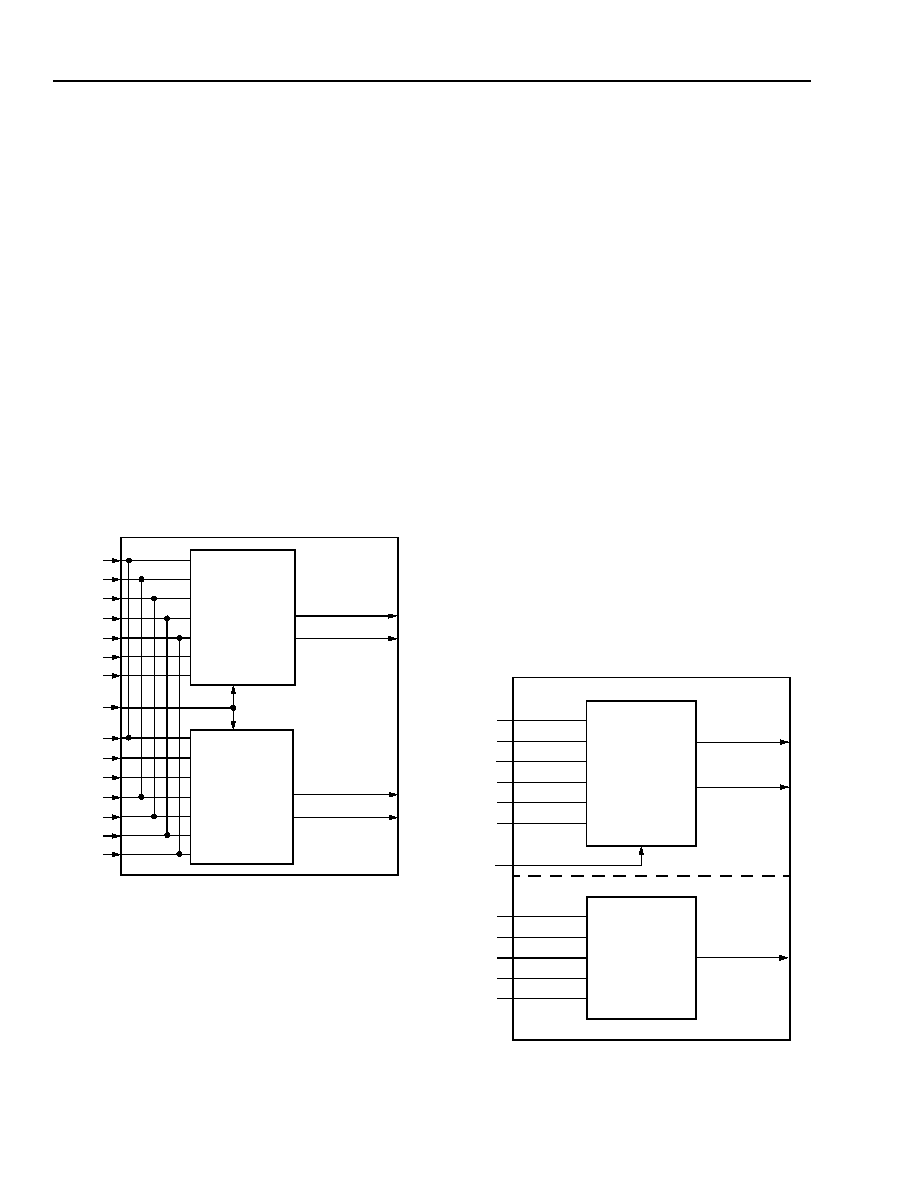
Figure 3. Simplified PFU Diagram
5-4573(F)
A4
A3
A2
A1
A4
A3
A2
A1
QLUT3
A0
CARRY
CARRY
A3
A2
A1
A0
QLUT2
B4
B3
B2
B1
B4
B3
B2
B1
QLUT1
B0
CARRY
CARRY
B3
B2
B1
B0
QLUT0
CIN
C0
LSR
GSR
WD[3:0]
CK
CKEN
TRI
PFU_XOR
B4
A4
PFU_NAND
PFU_MUX
C
C
C
C
WD3
WD2
WD1
WD0
C
C
C
T
T
T
T
REG3
SR
EN
REG2
SR
EN
REG1
SR
EN
REG0
SR
EN
O4
O3
O2
O1
O0
F3
C
C
COUT
F2
F1
F0
D0
D1
D2
D3
Q0
Q1
Q2
Q3
C
T
T
T
T
C
Figure 2 and Figure 3 show high-level and detailed
views of the ports in the PFU, respectively. The ports
are referenced with a two- to four-character suffix to a
PFU's location. As mentioned, there are two 5-bit input
data buses (A[4:0] and B[4:0]) to the LUT, one 4-bit
input data bus (WD[3:0]) to the latches/FFs, and an
output data bus (O[4:0]).
Figure 3 shows the four latches/FFs (REG[3:0]) and the
64-bit look-up table (QLUT[3:0]) in the PFU. The PFU
does combinatorial logic in the LUT and sequential
logic in the latches/FFs. The LUT is static random
access memory (SRAM) and can be used for read/
write or read-only memory. The eight 3-state buffers
found in each PLC are also shown, although they actu-
ally reside external to the PFU.
Each latch/FF can accept data from the LUT. Alterna-
tively, the latches/FFs can accept direct data from
WD[3:0], eliminating the LUT delay if no combinatorial
function is needed. The LUT outputs can bypass the
latches/FFs, which reduces the delay out of the PFU. It
is possible to use the LUT and latches/FFs more or
less independently. For example, the latches/FFs can
be used as a 4-bit shift register, and the LUT can be
used to detect when a register has a particular pattern
in it.

Lucent Technologies Inc.
7
Data Sheet
June 1999
ORCA Series 2 FPGAs
Programmable Logic Cells
(continued)
Table 3 lists the basic operating modes of the LUT. The
operating mode affects the functionality of the PFU
input and output ports and internal PFU routing. For
example, in some operating modes, the WD[3:0] inputs
are direct data inputs to the PFU latches/FFs. In the
dual 16 x 2 memory mode, the same WD[3:0] inputs
are used as a 4-bit data input bus into LUT memory.
The PFU is used in a variety of modes, as illustrated in
Figures 4 through 11, and it is these specific modes
that are most relevant to PFU functionality.
PFU Control Inputs
The four control inputs to the PFU are clock (CK), local
set/reset (LSR), clock enable (CE), and C0. The CK,
CE, and LSR inputs control the operation of all four
latches in the PFU. An active-low global set/reset
(GSRN) signal is also available to the latches/FFs in
every PFU. Their operation is discussed briefly here,
and in more detail in the Latches/Flip-Flops section.
The polarity of the control inputs can be inverted.
The CK input is distributed to each PFU from a vertical
or horizontal net. The CE input inhibits the latches/FFs
from responding to data inputs. The CE input can be
disabled, always enabling the clock. Each latch/FF can
be independently programmed to be set or reset by the
LSR and the global set/reset (GSRN) signals. Each
PFU's LSR input can be configured as synchronous or
asynchronous. The GSRN signal is always asynchro-
nous. The LSR signal applies to all four latches/FFs in
a PFU. The LSR input can be disabled (the default).
The asynchronous set/reset is dominant over clocked
inputs.
The C0 input is used as an input into the special PFU
gates for wide functions in combinatorial logic mode.
In the memory modes, this input is also used as the
write-port enable input. The C0 input can be disabled
(the default).
Look-Up Table Operating Modes
The look-up table (LUT) can be configured to operate
in one of three general modes:
s
Combinatorial logic mode
s
Ripple mode
s
Memory mode
The combinatorial logic mode uses a 64-bit look-up
table to implement Boolean functions. The two 5-bit
logic inputs, A[4:0] and B[4:0], and the C0 input are
used as LUT inputs. The use of these ports changes
based on the PFU operating mode.
The functionality of the LUT is determined by its operat-
ing mode. The entries in Table 3 show the basic modes
of operation for combinatorial logic, ripple, and memory
functions in the LUT. Depending on the operating
mode, the LUT can be divided into sub-LUTs. The LUT
is comprised of two 32-bit half look-up tables, HLUTA
and HLUTB. Each half look-up table (HLUT) is com-
prised of two quarter look-up tables (QLUTs). HLUTA
consists of QLUT2 and QLUT3, while HLUTB consists
of QLUT0 and QLUT1. The outputs of QLUT0, QLUT1,
QLUT2, and QLUT3 are F0, F1, F2, and F3, respec-
tively.
Table 3. Look-Up Table Operating Modes
For combinatorial logic, the LUT can be used to do any
single function of six inputs, any two functions of five
inputs, or four functions of four inputs (with some inputs
shared), and three special functions based on the two
five-input functions and C0.
Mode
Function
F4A
Two functions of four inputs, some inputs
shared (QLUT2/QLUT3)
F4B
Two functions of four inputs, some inputs
shared (QLUT0/QLUT1)
F5A
One function of five inputs (HLUTA)
F5B
One function of five inputs (HLUTB)
R
4-bit ripple (LUT)
MA
16 x 2 asynchronous memory (HLUTA)
MB
16 x 2 asynchronous memory (HLUTB)
SSPM 16 x 4 synchronous single-port memory
SDPM 16 x 2 synchronous dual-port memory
8
Lucent Technologies Inc.
Data Sheet
ORCA Series 2 FPGAs
June 1999
Programmable Logic Cells
(continued)
The LUT ripple mode operation offers standard arith-
metic functions, such as 4-bit adders, subtractors,
adder/subtractors, and counters. In the
ORCA
Series 2, there are two new ripple modes available.
The first new mode is a 4 x 1 multiplier, and the second
is a 4-bit comparator. These new modes offer the
advantages of faster speeds as well as denser logic
capabilities.
When the LUT is configured to operate in the memory
mode, a 16 x 2 asynchronous memory fits into an
HLUT. Both the MA and MB modes were available in
previous
ORCA
architectures, and each mode can be
configured in an HLUT separately. In the Series 2,
there are two new memory modes available. The first is
a 16 x 4 synchronous single-port memory (SSPM), and
the second is a 16 x 2 synchronous dual-port memory
(SDPM). These new modes offer easier implementa-
tion, faster speeds, denser RAMs, and a dual-port
capability that wasn't previously offered as an option in
the ATT2Cxx/ATT2Txx families.
If the LUT is configured to operate in the ripple mode, it
cannot be used for basic combinatorial logic or memory
functions. In modes other than the ripple, SSPM, and
SDPM modes, combinations of operating modes are
possible. For example, the LUT can be configured as a
16 x 2 RAM in one HLUT and a five-input combinatorial
logic function in the second HLUT. This can be done by
configuring HLUTA in the MA mode and HLUTB in the
F5B mode (or vice versa).
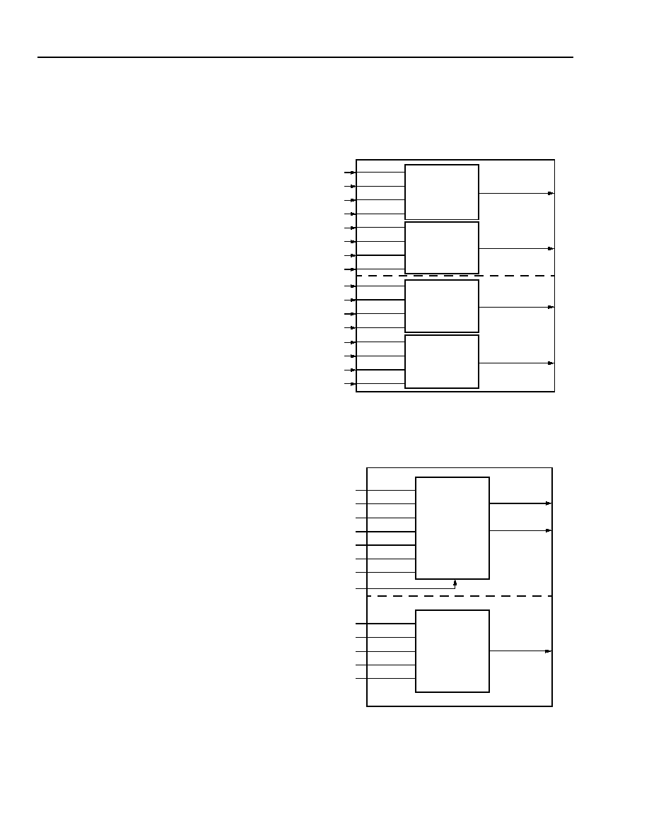
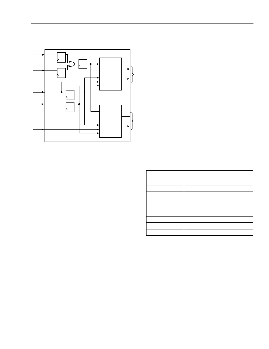
F4A/F4B Mode--Two Four-Input Functions
Each HLUT can be used to implement two four-input
combinatorial functions, but the total number of inputs
into each HLUT cannot exceed five. The two QLUTs
within each HLUT share three inputs. In HLUTA, the
A1, A2, and A3 inputs are shared by QLUT2 and
QLUT3. Similarly, in HLUTB, the B1, B2, and B3 inputs
are shared by QLUT0 and QLUT1. The four outputs
are F0, F1, F2, and F3. The results can be routed to
the D0, D1, D2, and D3 latch/FF inputs or as an output
of the PFU. The use of the LUT for four functions of up
to four inputs each is given in Figure 4.
F5A/F5B Mode--One Five-Input Variable Function
Each HLUT can be used to implement any five-input
combinatorial function. The input ports are A[4:0] and
B[4:0], and the output ports are F0 and F3. One five or
less input function is input into A[4:0], and the second
five or less input function is input into B[4:0]. The
results are routed to the latch/FF D0 and latch/FF D3
inputs, or as a PFU output. The use of the LUT for two
independent functions of up to five inputs is shown in
Figure 5. In this case, the LUT is configured in the F5A
and F5B modes. As a variation, the LUT can do one
function of up to five input variables and two four-input
functions using F5A and F4B modes or F4A and F5B
modes.
5-2753(F).r2
Figure 4. F4 Mode--Four Functions of Four-
Input Variables
5-2845(F).r2
Figure 5. F5 Mode--Two Functions of Five-Input
Variables
QLUT2
A3
A3
A2
A1
A0
A2
A1
A0
F2
QLUT3
A4
A4
A3
A2
A1
A3
A2
A1
F3
HLUTA
QLUT0
B3
B3
B2
B1
B0
B2
B1
B0
F0
QLUT1
B4
B4
B3
B2
B1
B3
B2
B1
F1
HLUTB
QLUT3
QLUT2
F3
QLUT1
QLUT0
B4
B3
B2
B1
B0
F0
WEA
A3
A2
A1
A0
B4
B3
B2
B1
B0
A4
A3
A2
A1
A0
HLUTA
HLUTB
c0
WPE
WD3
WD2
WD3
WD2
F2

Lucent Technologies Inc.
9
Data Sheet
June 1999
ORCA Series 2 FPGAs
Programmable Logic Cells
(continued)
F5M and F5X Modes--Special Function Modes
The PFU contains logic to implement two special func-
tion modes which are variations on the F5 mode. As
with the F5 mode, the LUT implements two indepen-
dent five-input functions. Figure 6 and Figure 7 show
the schematics for F5M and F5X modes, respectively.
The F5X and F5M functions differ from the basic F5A/
F5B functions in that there are three logic gates which
have inputs from the two 5-input LUT outputs. In some
cases, this can be used for faster and/or wider logic
functions.
As can be seen, two of the three inputs into the NAND,
XOR, and MUX gates, F0 and F3, are from the LUT.
The third input is from the C0 input into PFU. Since the
C0 input bypasses the LUTs, it has a much smaller
delay through the PFU than for all other inputs into the
special PFU gates. This allows multiple PFUs to be
cascaded together while reducing the delay of the criti-
cal path through the PFUs. The output of the first spe-
cial function (either XOR or MUX) is F1. Since the XOR
and MUX share the F1 output, the F5X and F5M
modes are mutually exclusive. The output of the NAND
PFU gate is F2 and is always available in either mode.
To use either the F5M or F5X functions, the LUT must
be in the F5A/F5B mode; i.e., only 5-input LUTs
allowed. In both the F5X and F5M functions, the out-
puts of the five-input combinatorial functions, F0 and
F3, are also usable simultaneously with the special
PFU gate outputs.
The output of the MUX is:
F1 = (HLUTA & C0) + (HLUTB &
C0
)
F1 = (F3 & C0) + (F0 &
C0
)
The output of the exclusive OR is:
F1 = HLUTA
HLUTB
C0
F1 = F3
F0
C0
The output of the NAND is:
F2 =
HLUTA & HLUTB & C0
F2 = F3 & F0 & C0
5-2754(F).r3
Figure 6. F5M Mode--Multiplexed Function of Two
Independent Five-Input Variable
Functions
5-2755(F).r2
Figure 7. F5X Mode--Exclusive OR Function of Two
Independent Five-Input Variable
Functions
QLUT3
QLUT2
A4
A4
A3
A2
A1
A0
A3
A2
A1
A0
QLUT1
QLUT0
B4
B4
B3
B2
B1
B0
B3
B2
B1
B0
C0
F3
F0
F1
F0
F2
F3
A4
A4
A3
A2
A1
A0
A3
A2
A1
A0
B4
B4
B3
B2
B1
B0
B3
B2
B1
B0
C0
F3
F0
F1
F0
F2
F3
HLUTA
HLUTB
10
Lucent Technologies Inc.
Data Sheet
ORCA Series 2 FPGAs
June 1999
Programmable Logic Cells
(continued)
5-2751(F).r3
Figure 8. F5M Mode--One Six-Input Variable
Function
F5M Mode--One Six-Input Variable Function
The LUT can be used to implement any function of six-
input variables. As shown in Figure 8, five input signals
(A[4:0]) are routed into both the A[4:0] and B[4:0] ports,
and the C0 port is used for the sixth input. The output
port is F1.
Ripple Mode
The LUT can do nibble-wide ripple functions with high-
speed carry logic. Each QLUT has a dedicated carry-
out net to route the carry to/from the adjacent QLUT.
Using the internal carry circuits, fast arithmetic and
counter functions can be implemented in one PFU.
Similarly, each PFU has carry-in (CIN) and carry-out
(COUT) ports for fast-carry routing between adjacent
PFUs.
The ripple mode is generally used in operations on two
4-bit buses. Each QLUT has two operands and a ripple
(generally carry) input, and provides a result and ripple
(generally carry) output. A single bit is rippled from the
previous QLUT and is used as input into the current
QLUT. For QLUT0, the ripple input is from the PFU CIN
port. The CIN data can come from either the fast-carry
routing or the PFU input B4, or it can be tied to logic 1
or logic 0.
The resulting output and ripple output are calculated by
using generate/propagate circuitry. In ripple mode, the
two operands are input into A[3:0] and B[3:0]. The four
result bits, one per QLUT, are F[3:0] (see Figure 9).
The ripple output from QLUT3 can be routed to dedi-
cated carry-out circuitry into any of four adjacent PLCs,
or it can be placed on the O4 PFU output, or both. This
allows the PLCs to be cascaded in the ripple mode so
that nibble-wide ripple functions can be expanded eas-
ily to any length.
5-2756(F).r32
Figure 9. Ripple Mode
The ripple mode can be used in one of four submodes.
The first of these is adder/subtractor mode. In this
mode, each QLUT generates two separate outputs.
One of the two outputs selects whether the carry-in is
to be propagated to the carry-out of the current QLUT
or if the carry-out needs to be generated. The result of
this selection is placed on the carry-out signal, which is
connected to the next QLUT or the COUT signal, if it is
the last QLUT (QLUT3).
The other QLUT output creates the result bit for each
QLUT that is connected to F[3:0]. If an adder/subtractor
is needed, the control signal to select addition or sub-
traction is input on A4. The result bit is created in one-
half of the QLUT from a single bit from each input bus,
along with the ripple input bit. These inputs are also
used to create the programmable propagate.
QLUT3
QLUT2
A4
A4
A3
A2
A1
A0
A3
A2
A1
A0
QLUT1
QLUT0
B4
B4
B3
B2
B1
B0
B3
B2
B1
B0
C0
F3
F0
F1
QLUT3
B3
B3
A3
A3
F3
QLUT2
B2
B2
A2
A2
F2
QLUT1
B1
B1
A1
A1
F1
QLUT0
B0
B0
A0
A0
F0
CIN
CIN
COUT
COUT

Lucent Technologies Inc.
11
Data Sheet
June 1999
ORCA Series 2 FPGAs
Programmable Logic Cells
(continued)
The second submode is the counter submode (see
Figure 10). The present count is supplied to input
A[3:0], and then output F[3:0] will either be incre-
mented by one for an up counter or decremented by
one for a down counter. If an up counter or down
counter is needed, the control signal to select the direc-
tion (up or down) is input on A4. Generally, the latches/
FFs in the same PFU are used to hold the present
count value.
5-4643(F).r1
Figure 10. Counter Submode with Flip-Flops
In the third submode, multiplier submode, a single
PFU can affect a 4 x 1-bit multiply and sum with a par-
tial product (see Figure 11). The multiplier bit is input at
A4, and the multiplicand bits are input at B[3:0], where
B3 is the most significant bit (MSB). A[3:0] contains the
partial product (or other input to be summed) from a
previous stage. If A4 is logical 1, the multiplicand is
added to the partial product. If A4 is logical zero, zero is
added to the partial product, which is the same as
passing the partial product. CIN can hold the carry-in
from the less significant PFUs if the multiplicand is
wider than 4 bits, and COUT holds any carry-out from
the addition, which may then be used as part of the
product or routed to another PFU in multiplier mode for
multiplicand width expansion.
Figure 11. Multiplier Submode
Ripple mode's fourth submode features equality
comparators, where one 4-bit bus is input on B[3:0],
another 4-bit bus is input on B[3:0], and the carry-in is
tied to 0 inside the PFU. The carry-out (¶) signal will be
0 if A = B or will be 1 if A ¶ B. If larger than 4 bits, the
carry-out (¶) signal can be cascaded using fast-carry
logic to the carry-in of any adjacent PFU. Comparators
for greater than or equal or less than (>, =, <) continue
to be supported using the ripple mode subtractor. The
use of this submode could be shown using Figure 9
with CIN tied to 0.
D Q
COUT
LUT
A3
QLUT3
F3
Q3
COUT
D Q
A2
QLUT2
F2
Q2
D Q
A1
QLUT1
F1
Q1
D Q
A0
QLUT0
F0
Q0
CIN
CIN
+
1 0
A3
B3
0
A4
COUT
F3
+
A2
B2
F2
+
A1
B1
F1
+
A0
B0
F0
CIN
1 0
0
1 0
0
1 0
0
5-4620(F)
12
Lucent Technologies Inc.
Data Sheet
ORCA Series 2 FPGAs
June 1999
Programmable Logic Cells
(continued)
Asynchronous Memory Modes--MA and MB
The LUT in the PFU can be configured as either read/
write or read-only memory. A read/write address
(A[3:0], B[3:0]), write data (WD[1:0], WD[3:2]), and two
write-enable (WE) ports are used for memory. In asyn-
chronous memory mode, each HLUT can be used as a
16 x 2 memory. Each HLUT is configured indepen-
dently, allowing functions such as a 16 x 2 memory in
one HLUT and a logic function of five input variables or
less in the other HLUT.
Figure 12 illustrates the use of the LUT for a 16 x 4
memory. When the LUTs are used as memory, there
are independent address, input data, and output data
buses. If the LUT is used as a 16 x 4 read/write mem-
ory, the A[3:0] and B[3:0] ports are address inputs
(A[3:0]). The A4 and B4 ports are write-enable (WE)
signals. The WD[3:0] inputs are the data inputs. The
F[3:0] data outputs can be routed out on the O[4:0]
PFU outputs or to the latch/FF D[3:0] inputs.
5-2757(F).r3
Figure 12. MA/MB Mode--16 x 4 RAM
To increase memory word depth above 16 (e.g., 32 x
4), two or more PLCs can be used. The address and
write data inputs for the two or more PLCs are tied
together (bit by bit), and the data outputs are routed
through the four 3-statable BIDIs available in each PFU
and are then tied together (bit by bit).
The control signal of the 3-statable BIDIs, called a RAM
bank-enable, is created from a decode of upper
address bits. The RAM bank-enable is then used to
enable 4 bits of data from a PLC onto the read data
bus.
The
ORCA
Series 2 series also has a new AND func-
tion available for each PFU in RAM mode. The inputs to
this function are the write-enable (WE) signal and the
write-port enable (WPE) signal. The write-enable sig-
nal is A4 for HLUTA and B4 for HLUTB, while the other
input into the AND gates for both HLUTs is the write-
port enable, input on C0 or CIN. Generally, the WPE
input is driven by the same RAM bank-enable signal
that controls the BIDIs in each PFU.
The selection of which RAM bank to write data into
does not require the use of LUTs from other PFUs, as
in previous
ORCA
architectures. This reduces the num-
ber of PFUs required for RAMs larger than 16 words in
depth. Note that if either HLUT is in MA/MB mode, then
the same WPE is active for both HLUTs.
To increase the memory's word size (e.g., 16 x 8), two
or more PLCs are used again. The address, write-
enable, and write-port enable of the PLCs are tied
together (bit by bit), and the data is different for each
PLC. Increasing both the address locations and word
size is done by using a combination of these two tech-
niques.
The LUT can be used simultaneously for both memory
and a combinatorial logic function. Figure 13 shows the
use of a LUT implementing a 16 x 2 RAM (HLUTA) and
any function of up to five input variables (HLUTB).
5-2845(F).a.r1
Figure 13. MA/F5 Mode--16 x 2 Memory and One
Function of Five Input Variables
A3
A3
A2
A1
A0
WD3
A2
A1
A0
WD3
F3
F2
WD2
WD2
WD1
WD0
B3
B2
B1
WD0
B3
B2
B1
F1
F0
B0
B0
WD1
A4
B4
WEA
WEB
HLUTA
HLUTB
WPE
C0
C0
QLUT3
QLUT2
F3
QLUT1
QLUT0
B4
B3
B2
B1
B0
F0
WEA
A3
A2
A1
A0
B4
B3
B2
B1
B0
A4
A3
A2
A1
A0
HLUTA
HLUTB
F2
WD3
WPE
WD3
C0

Lucent Technologies Inc.
13
Data Sheet
June 1999
ORCA Series 2 FPGAs
Programmable Logic Cells
(continued)
Synchronous Memory Modes--SSPM and SDPM
The MA/MB asynchronous memory modes described
previously allow the PFU to perform as a 16 x 4
(64 bits) single-port RAM. Synchronously writing to this
RAM requires the write-enable control signal to be
gated with the clock in another PFU to create a write
pulse. To simplify this functionality, the Series 2 devices
contain a synchronous single-port memory (SSPM)
mode, where the generation of the write pulse is done
in each PFU.
With SSPM mode, the entire LUT becomes a 16 x 4
RAM, as shown in Figure 14. In this mode, the input
ports are write enable (WE), write-port enable (WPE),
read/write address (A[3:0]), and write data (WD[3:0]).
To synchronously write the RAM, WE (input into a4)
and WPE (input into either C0 or CIN) are latched and
ANDed together. The result of this AND function is sent
to a pulse generator in the LUT, which writes the RAM
synchronous to the RAM clock. This RAM clock is the
same one sent to the PFU latches/FFs; however, if nec-
essary, it can be programmably inverted.
5-4642(F).r1
Figure 14. SSPM Mode--16 x 4 Synchronous
Single-Port Memory
The write address (WA[3:0]) and write data (WD[3:0])
are also latched by the RAM clock in order to simplify
the timing. Reading data from the RAM is done asyn-
chronously; thus, the read address (RA[3:0]) is not
latched. The result from the read operation is placed on
the LUT outputs (F[3:0]). The F[3:0] data outputs can
be routed out of the PFU or sent to the latch/FF D[3:0]
inputs.
There are two ways to use the latches/FFs in conjunc-
tion with the SSPM. If the phase of the latch/FF clock
and the RAM clock are the same, only a read address
or write address can be supplied to the RAM that
meets the synchronous timing requirements of both
the RAM clock and latch/FF clock. Therefore, either a
write to the RAM or a read from the RAM can be done
in each clock cycle, but not both. If the RAM clock is
inverted from the latch/FF clock, then both a write to
the RAM and a read from the RAM can occur in each
clock cycle. This is done by adding an external write
address/read address multiplexer as shown in
Figure 15.
The write address is supplied on the phase of the clock
that allows for setup to the RAM clock, and the read
address is supplied on the phase of the clock that
allows the read data to be set up to the latch/FF clock.
If a higher-speed RAM is required that allows both a
read and write in each clock cycle, the synchronous
dual-port memory mode (SDPM) can be used, since it
does not require the use of an external multiplexer.
5-4644(F).r1
Figure 15. SSPM with Read/Write per Clock Cycle
WE
WPE
A4
D Q
D Q
CIN, C0
A[3:0]
WD[3:0]
WR
WA[3:0]
RA[3:0]
WD[3:2]
HLUTA
F3
F2
D Q
D Q
WR
WA[3:0]
RA[3:0]
WD[1:0]
HLUTB
F1
F0
WRITE PULSE
GENERATOR
A[3:0], B[3:0]
WD[3:0]
WE
A
WD
RAM CLK
WRITE ADDRESS
READ ADDRESS
0
1
WPE
SSPM
CLOCK
D
Q
PFU

Data Sheet
ORCA Series 2 FPGAs
June 1999
14
Lucent Technologies Inc.
Programmable Logic Cells
(continued)
Note: The lower address bits are not shown.
Figure 16. Synchronous RAM with Write-Port Enable (WPE)
UPPER
ADDRESS
BITS
ADDRESS
DECODE
LUT1
BANK_EN1
UPPER
ADDRESS
BITS
ADDRESS
DECODE
LUT2
BANK_EN2
WR
DI
WPE
DO
16 x 4 RAM +
4 BUFFERS/PFU
BIDI
DOUT
4
WR
DI
WPE
DO
16 x 4 RAM +
4 BUFFERS/PFU
DIN
WR
CLK
4
BIDI
4
4
5-4640(F)
To increase memory word depth above 16 (e.g., 32 x
4), two or more PLCs can be used. The address and
write data inputs for the two or more PLCs are tied
together (bit by bit), and the data outputs are routed
through the four 3-statable BIDIs available in each
PFU. The BIDI outputs are then tied together (bit by
bit), as seen in Figure 16.
The control signals of the 3-statable BIDIs, called RAM
bank-enable (BANK_EN1 and BANK_EN2), are cre-
ated from a decode of upper address bits. The RAM
bank-enable is then used to enable 4 bits of data from
a PLC onto the read data (DOUT) bus.
The Series 2 series now has a new AND function avail-
able for each PFU in RAM mode. The inputs to this
function are the write-enable (WE) signal and the write-
port enable (WPE) signal. The write-enable signal is
input on A4, while the write-port enable is input on C0
or CIN. Generally, the WPE input is driven by the same
RAM bank-enable signal that controls the BIDIs in each
PFU.
The selection as to which RAM bank to write data into
does not require the use of LUTs from other PFUs, as
in previous
ORCA
architectures. This reduces the num-
ber of PFUs required for RAMs larger than 16 words in
depth.
A special use of this method can be to increase word
depth to 32 words. Since both the WPE input into the
RAM and the 3-state input into the BIDI can be
inverted, a decode of the one upper address bit is not
required. Instead, the bank-enable signal for both
banks is tied to the upper address bit, with the WPE
and 3-state inputs active-high for one bank and active-
low for the other.
To increase the memory's word size (e.g., 16 x 8), two
or more PLCs are used again. The address, write-
enable, and write-port enable of the PLCs are tied
together (bit by bit), and the data is different for each
PLC. Increasing both the address locations and word
size is accomplished by using a combination of these
two techniques.
Lucent Technologies Inc.
15
Data Sheet
June 1999
ORCA Series 2 FPGAs
Programmable Logic Cells
(continued)
5-4641(F).r1
Figure 17. SDPM Mode--16 x 2 Synchronous
Dual-Port Memory
The Series 2 devices have added a second synchro-
nous memory mode known as the synchronous dual-
port memory (SDPM) mode. This mode writes data
into the memory synchronously in the same manner
described previously for SSPM mode. The SDPM
mode differs in that two separate 16 x 2 memories are
created in each PFU that have the same WE, WPE,
write data (WD[1:0]), and write address (WA[3:0])
inputs, as shown in Figure 17.
The outputs of HLUTA (F[3:2]) operate the same way
they do in SSPM mode--the read address comes
directly from the A[3:0] inputs used to create the
latched write address. The outputs of HLUTB (F[1:0])
operate in a dual-port mode where the write address
comes from the latched version of A[3:0], and the read
address comes directly from RA[3:0], which is input on
B[3:0].
Since external multiplexing of the write address and
read address is not required, extremely fast RAMs can
be created. New system applications that require an
interface between two different asynchronous clocks
can also be implemented using the SDPM mode. An
example of this is accomplished by creating FIFOs
where one clock controls the synchronous write of data
into the FIFO, and the other clock controls the read
address to allow reading of data at any time from the
FIFO.
Latches/Flip-Flops
The four latches/FFs in the PFU can be used in a vari-
ety of configurations. In some cases, the configuration
options apply to all four latches/FFs in the PFU. For
other options, each latch/FF is independently program-
mable.
Table 4 summarizes these latch/FF options. The
latches/FFs can be configured as either positive or
negative level-sensitive latches, or positive or negative
edge-triggered flip-flops. All latches/FFs in a given PFU
share the same clock, and the clock to these latches/
FFs can be inverted. The input into each latch/FF is
from either the corresponding QLUT output (F[3:0]) or
the direct data input (WD[3:0]). For latches/FFs located
in the two outer rings of PLCs, additional inputs are
possible. These additional inputs are fast paths from
I/O pads located in PICs in the same row or column as
the PLCs. If the latch/FF is not located in the two outer
rings of the PLCs, the latch/FF input can also be tied to
logic 0, which is the default. The four latch/FF outputs,
Q[3:0], can be placed on the five PFU outputs, O[4:0].
Table 4. Configuration RAM Controlled Latch/
Flip-Flop Operation
The four latches/FFs in a PFU share the clock (CK),
clock enable (CE), and local set/reset (LSR) inputs.
When CE is disabled, each latch/FF retains its previous
value when clocked. Both the clock enable and LSR
inputs can be inverted to be active-low.
WE
WPE
A4
D Q
D Q
CIN, C0
WA[3:0]
WD[1:0]
WR
WA[3:0]
RA[3:0]
WD[1:0]
HLUTA
F3
F2
D Q
D Q
WR
WA[3:0]
RA[3:0]
WD[1:0]
HLUTB
F1
F0
WRITE PULSE
GENERATOR
A[3:0]
WD[1:0]
RA[3:0] B[3:0]
SS
PM OUTPU
T
SD
P
M
O
U
TP
U
T
Function Options
Functionality Common to All Latch/FFs in PFU
LSR Operation
Asynchronous or synchronous
Clock Polarity
Noninverted or inverted
Front-End Select
Direct (WD[3:0]) or from LUT
(F[3:0])
LSR Priority
Either LSR or CE has priority
Functionality Set Individually in Each Latch/FF in PFU
Latch/FF Mode
Latch or flip-flop
Set/Reset Mode
Set or Reset

Data Sheet
ORCA Series 2 FPGAs
June 1999
16
Lucent Technologies Inc.
Programmable Logic Cells
(continued)
The set/reset operation of the latch/FF is controlled by
two parameters: reset mode and set/reset value. When
the global set/reset (GSRN) or local set/reset (LSR) are
inactive, the storage element operates normally as a
latch or FF. The reset mode is used to select a synchro-
nous or asynchronous LSR operation. If synchronous,
LSR is enabled only if clock enable (CE) is active. For
the Series 2 series, a new option called the LSR prior-
ity allows the synchronous LSR to have priority over the
CE input, thereby setting or resetting the FF indepen-
dent of the state of CE. The clock enable is supported
on FFs, not latches. The clock enable function is imple-
mented by using a two-input multiplexer on the FF
input, with one input being the previous state of the FF
and the other input being the new data applied to the
FF. The select of this two-input multiplexer is clock
enable (CE), which selects either the new data or the
previous state. When CE is inactive, the FF output
does not change when the clock edge arrives.
The GSRN signal is only asynchronous, and it sets/
resets all latches/FFs in the FPGA based upon the set/
reset configuration bit for each latch/FF. The set/reset
value determines whether GSRN and LSR are set or
reset inputs. The set/reset value is independent for
each latch/FF.
If the local set/reset is not needed, the latch/FF can be
configured to have a data front-end select. Two data
inputs are possible in the front-end select mode, with
the LSR signal used to select which data input is used.
The data input into each latch/FF is from the output of
its associated QLUT F[3:0] or direct from WD[3:0],
bypassing the LUT. In the front-end data select mode,
both signals are available to the latches/FFs.
For PLCs that are in the two outside rows or columns of
the array, the latch/FFs can have two inputs in addition
to the F and WD inputs mentioned above. One input is
from an I/O pad located at the PIC closest to either the
left or right of the given PLC (if the PLC is in the left two
columns or right two columns of the array). The other
input is from an I/O pad located at the closest PIC
either above or below the given PLC (if the PLC is in
the top or the bottom two rows). It should be noted that
both inputs are available for a 2 x 2 array of PLCs in
each corner of the array. For the entire array of PLCs, if
either or both of these inputs is unavailable, the latch/
FF data input can be tied to a logic 0 instead (the
default).
To speed up the interface between signals external to
the FPGA and the latches/FFs, there are direct paths
from latch/FF outputs to the I/O pads. This is done for
each PLC that is adjacent to a PIC.
The latches/FFs can be configured in three modes:
1. Local synchronous set/reset: the input into the PFU's
LSR port is used to synchronously set or reset each
latch/FF.
2. Local asynchronous set/reset: the input into LSR
asynchronously sets or resets each latch/FF.
3. Latch/FF with front-end select: the data select signal
(actually LSR) selects the input into the latches/FFs
between the LUT output and direct data in.
For all three modes, each latch/FF can be indepen-
dently programmed as either set or reset. Each latch/
FF in the PFU is independently configured to operate
as either a latch or flip-flop. Figure 18 provides the logic
functionality of the front-end select, global set/reset,
and local set/reset operations.
Note: CD = configuration data.
5-2839(F).a
Figure 18. Latch/FF Set/Reset Configurations
CE
D
S_SET
S_RESET
CLK
SET RESET
Q
LSR
GSRN
CD
CE
D
CLK
SET RESET
LSR
CD
CE
CE
D
CLK
SET RESET
CD
CE
CE
WD
LSR
GSRN
PDINLR
LOGIC 0
WD
F
LOGIC 0
WD
GSRN
Q
Q
PDINTB
F
PDINLR
PDINTB
F
LOGIC 0
WD
PDINLR
PDINTB

Lucent Technologies Inc.
17
Data Sheet
June 1999
ORCA Series 2 FPGAs
Programmable Logic Cells
(continued)
PLC Routing Resources
Generally, the
ORCA
Foundry
Development System is
used to automatically route interconnections. Interac-
tive routing with the
ORCA
Foundry design editor
(EPIC) is also available for design optimization. To use
EPIC for interactive layout, an understanding of the
routing resources is needed and is provided in this sec-
tion.
The routing resources consist of switching circuitry and
metal interconnect segments. Generally, the metal lines
which carry the signals are designated as routing
nodes (lines). The switching circuitry connects the rout-
ing nodes, providing one or more of three basic func-
tions: signal switching, amplification, and isolation. A
net running from a PFU or PIC output (source) to a
PLC or PIC input (destination) consists of one or more
lines, connected by switching circuitry designated as
configurable interconnect points (CIPs).
The following sections discuss PLC, PIC, and interquad
routing resources. This section discusses the PLC
switching circuitry, intra-PLC routing, inter-PLC routing,
and clock distribution.
Configurable Interconnect Points
The process of connecting lines uses three basic types
of switching circuits: two types of configurable intercon-
nect points (CIPs) and bidirectional buffers (BIDIs). The
basic element in CIPs is one or more pass transistors,
each controlled by a configuration RAM bit. The two
types of CIPs are the mutually exclusive (or multi-
plexed) CIP and the independent CIP.
A mutually exclusive set of CIPs contains two or more
CIPs, only one of which can be on at a time. An inde-
pendent CIP has no such restrictions and can be on
independent of the state of other CIPs. Figure 19
shows an example of both types of CIPs.
f.13(F)
Figure 19. Configurable Interconnect Point
3-Statable Bidirectional Buffers
Bidirectional buffers provide isolation as well as amplifi-
cation for signals routed a long distance. Bidirectional
buffers are also used to drive signals directly onto
either vertical or horizontal XL and XH lines (to be
described later in the inter-PLC routing section). BIDIs
are also used to indirectly route signals through the
switching lines. Any number from zero to eight BIDIs
can be used in a given PLC.
The BIDIs in a PLC are divided into two nibble-wide
sets of four (BIDI and BIDIH). Each of these sets has a
separate BIDI controller that can have an application
net connected to its TRI input, which is used to 3-state
enable the BIDIs. Although only one application net can
be connected to both BIDI controllers, the sense of this
signal (active-high, active-low, or ignored) can be con-
figured independently. Therefore, one set can be used
for driving signals, the other set can be used to create
3-state buses, both sets can be used for 3-state buses,
and so forth.
2
INDEPENDENT CIP
CD
A
B
A
B
=
MULTIPLEXED CIP
A
B
C
A
B
C
O
O
CD

18
Lucent Technologies Inc.
Data Sheet
ORCA Series 2 FPGAs
June 1999
Programmable Logic Cells
(continued)
5-4479p2(F)
Figure 20. 3-Statable Bidirectional Buffers
Intra-PLC Routing
The function of the intra-PLC routing resources is to
connect the PFU's input and output ports to the routing
resources used for entry to and exit from the PLC.
These are nets for providing PFU feedback, turning
corners, or switching from one type of routing resource
to another.
PFU Input and Output Ports. There are 19 input ports
to each PFU. The PFU input ports are labeled A[4:0],
B[4:0], WD[3:0], C0, CK, LSR, CIN, and CE. The six
output ports are O[4:0] and COUT. These ports corre-
spond to those described in the PFU section.
Switching Lines. There are four sets of switching lines
in each PLC, one in each corner. Each set consists of
five switching elements, labeled SUL[4:0], SUR[4:0],
SLL[4:0], and SLR[4:0], for the upper-left, upper-right,
lower-left, and lower-right sections of the PFUs,
respectively. The switching lines connect to the PFU
inputs and outputs as well as the BIDI and BIDIH lines,
to be described later. They also connect to both the
horizontal and vertical X1 and X4 lines (inter-PLC rout-
ing resources, described below) in their specific corner.
One of the four sets of switching lines can be con-
nected to a set of switching lines in each of the four
adjacent PLCs or PICs. This allows direct routing of up
to five signals without using inter-PLC routing.
BIDI/BIDIH Lines. There are two sets of bidirectional
lines in the PLC, each set consisting of four bidirec-
tional buffers. They are designated BIDI and BIDIH and
have similar functionality. The BIDI lines are used in
conjunction with the XL lines, and the BIDIH lines are
used in conjunction with the XH lines. Each side of the
four BIDIs in the PLC is connected to a BIDI line on the
left (BL[3:0]) and on the right (BR[3:0]). These lines can
be connected to the XL lines through CIPs, with BL[3:0]
connected to the vertical XL lines and BR[3:0] con-
nected to the horizontal XL lines. Both BL[3:0] and
BR[3:0] have CIPs which connect to the switching lines.
Similarly, each side of the four BIDIHs is connected to a
BIDIH line: BLH[3:0] on the left and BRH[3:0] on the
right. These lines can also be connected to the XH
lines through CIPs, with BLH[3:0] connected to the ver-
tical XH lines and BRH[3:0] connected to the horizontal
XH lines. Both BLH[3:0] and BRH[3:0] have CIPs which
connect to the switching lines.
CIPs are also provided to connect the BIDIH and BIDIL
lines together on each side of the BIDIs. For example,
BLH3 can connect to BL3, while BRH3 can connect to
BR3.
RIGHT-LEFT BIDI
LEFT-RIGHT BIDI
UNUSED BIDI
LEFT-RIGHT BIDI
BIDI
CONTROLLER
TRI
RIGHT-LEFT BIDIH
LEFT-RIGHT BIDIH
UNUSED BIDIH
LEFT-RIGHT BIDIH
BIDIH
CONTROLLER

Lucent Technologies Inc.
19
Data Sheet
June 1999
ORCA Series 2 FPGAs
Programmable Logic Cells
(continued)
Inter-PLC Routing Resources
The inter-PLC routing is used to route signals between
PLCs. The lines occur in groups of four, and differ in the
numbers of PLCs spanned. The X1 lines span one
PLC, the X4 lines span four PLCs, the XH lines span
one-half the width (height) of the PLC array, and the XL
lines span the width (height) of the PLC array. All types
of lines run in both horizontal and vertical directions.
Table 5 shows the groups of inter-PLC lines in each
PLC. In the table, there are two rows/columns each for
X1 and X4 lines. In the design editor, the horizontal X1
and X4 lines are located above and below the PFU.
Similarly, the vertical segments are located on each
side. The XL and XH lines only run below and to the left
of the PFU. The indexes specify individual lines within a
group. For example, the VX4[2] line runs vertically to
the left of the PFU, spans four PLCs, and is the third
line in the 4-bit wide bus.
Table 5. Inter-PLC Routing Resources
Figure 21 shows the inter-PLC routing within one PLC.
Figure 22 provides a global view of inter-PLC routing
resources across multiple PLCs.
5-4528(F)
Figure 21. Single PLC View of Inter-PLC Lines
X1 Lines. There are a total of 16 X1 lines per PLC:
eight vertical and eight horizontal. Each of these is sub-
divided into nibble-wide buses: HX1[3:0], HX1[7:4],
VX1[3:0], and VX1[7:4]. An X1 line is one PLC long.
If a net is longer than one PLC, an X1 line can be
lengthened to n times its length by turning on n ≠ 1
CIPs. A signal is routed onto an X1 line via the switch-
ing lines.
X4 Lines. There are four sets of four X4 lines, for a
total of 16 X4 lines per PLC. They are HX4[3:0],
HX4[7:4], VX4[3:0], and VX4[7:4]. Each set of X4 lines
is twisted each time it passes through a PLC, and one
of the four is broken with a CIP. This allows a signal to
be routed for a length of four cells in any direction on a
single line without additional CIPs. The X4 lines can be
used to route any nets that require minimum delay. A
longer net is routed by connecting two X4 lines
together by a CIP. The X4 lines are accessed via the
switching lines.
Horizontal
Lines
Vertical
Lines
Distance
Spanned
HX1[3:0]
VX1[3:0]
One PLC
HX1[7:4]
VX1[7:4]
One PLC
HX4[3:0]
VX4[3:0]
Four PLCs
HX4[7:4]
VX4[7:4]
Four PLCs
HXL[3:0]
VXL[3:0]
PLC Array
HXH[3:0]
VXH[3:0]
1/2 PLC Array
CKL, CKR
CKT, CKB
PLC Array
PROGRAMMABLE
FUNCTION UNIT
DIRECT[4:0]
HX4[7:4]
HX1[7:4]
DIRECT[4:0]
HXH[3:0]
HX1[3:0]
DIRECT[4:0]
DIRECT[4:0]
HX4[3:0]
VX4
[7
:4
]
VX
1[
7:
4]
V
X
L[
3:
0]
V
X
1
[3
:0]
VX
4[
3:
0]
V
X
H
[3
:0
]
CK
B
,
CK
T
HXL[3:0]
CKL, CKR

20
Lucent Technologies Inc.
Data Sheet
ORCA Series 2 FPGAs
June 1999
Programmable Logic Cells
(continued)
XL Lines. The long XL lines run vertically and horizon-
tally the height and width of the array, respectively.
There are a total of eight XL lines per PLC: four hori-
zontal (HXL[3:0]) and four vertical (VXL[3:0]). Each
PLC column has four XL lines, and each PLC row has
four XL lines. Each of the XL lines connects to the two
PICs at either end. The Series 2, which consists of a
18 x 18 array of PLCs, contains 72 VXL and 72 HXL
lines. They are intended primarily for global signals
which must travel long distances and require minimum
delay and/or skew, such as clocks.
There are three methods for routing signals onto the XL
lines. In each PLC, there are two long-line drivers: one
for a horizontal XL line, and one for a vertical XL line.
Using the long-line drivers produces the least delay.
The XL lines can also be driven directly by PFU outputs
using the BIDI lines. In the third method, the XL lines
are accessed by the bidirectional buffers, again using
the BIDI lines.
XH Lines. Four by half (XH) lines run horizontally and
four XH lines run vertically in each row and column in
the array. These lines travel a distance of one-half the
PLC array before being broken in the middle of the
array, where they connect to the interquad block (dis-
cussed later). They also connect at the periphery of the
FPGA to the PICs, like the XL lines. The XH lines do
not twist like XL lines, allowing nibble-wide buses to be
routed easily.
Two of the three methods of routing signals onto the
XL lines can also be used for the XH lines. A special
XH line driver is not supplied for the XH lines.
Clock Lines. For a very fast and low-skew clock (or
other global signal tree), clock lines run the entire
height and width of the PLC array. There are two hori-
zontal clock lines per PLC row (CKL, CKR) and two
vertical clock lines per PLC column (CKT, CKB). The
source for these clock lines can be any of the four I/O
buffers in the PIC. The horizontal clock lines in a row
(CKL, CKR) are driven by the left and right PICs,
respectively. The vertical clock lines in a column (CKT,
CKB) are driven by the top and bottom PICs, respec-
tively.
The clock lines are designed to be a clock spine. In
each PLC, there is a fast connection available from the
clock line to the long-line driver (described earlier).
With this connection, one of the clock lines in each PLC
can be used to drive one of the four XL lines perpendic-
ular to it, which, in turn, creates a clock tree.
This feature is discussed in detail in the Clock Distribu-
tion Network section.
Minimizing Routing Delay
The CIP is an active element used to connect two lines.
As an active element, it adds significantly to the resis-
tance and capacitance of a net, thus increasing the
net's delay. The advantage of the X1 line over a X4 line
is routing flexibility. A net from PLC db to PLC cb is eas-
ily routed by using X1 lines. As more CIPs are added to
a net, the delay increases. To increase speed, routes
that are greater than two PLCs away are routed on the
X4 lines because a CIP is located only in every fourth
PLC. A net that spans eight PLCs requires seven X1
lines and six CIPs. Using X4 lines, the same net uses
two lines and one CIP.
All routing resources in the PLC can carry 4-bit buses.
In order for data to be used at a destination PLC that is
in data path mode, the data must arrive unscrambled.
For example, in data path operation, the least signifi-
cant bit 0 must arrive at either A[0] or B[0]. If the bus is
to be routed by using either X4 or XL lines (both of
which twist as they propagate), the bus must be placed
on the appropriate lines at the source PLC so that the
data arrives at the destination unscrambled. The
switching lines provide the most efficient means of con-
necting adjacent PLCs. Signals routed with these lines
have minimum propagation delay.
Data Sheet
June 1999
ORCA Series 2 FPGAs
Lucent Technologies Inc.
21
Programmable Logic Cells
(continued)
5-2841(F)2C.r9
Figure 22. Multiple PLC View of Inter-PLC Routing
PFU
PFU
PFU
PFU
PFU
PFU
PFU
PFU
PFU
SHOWS PLCs
CKR
CKL
CKR
CKL
HX4[4]
HX4[5]
HX4[6]
HX4[7]
HX1[7:4]
HX4[5]
HX4[6]
HX4[7]
HX4[4]
HXL[0]
HXL[1]
HXL[2]
HXL[3]
HX1[3:0]
HX4[0]
HX4[1]
HX4[2]
HX4[3]
HXL[3]
HXL[0]
HXL[1]
HXL[2]
HX4[1]
HX4[2]
HX4[3]
HX4[0]
HX4[4]
HX4[5]
HX4[6]
HX4[7]
HX1[7:4]
HX4[5]
HX4[6]
HX4[7]
HX4[4]
HX1[7:4]
HX4[4]
HX4[5]
HX4[6]
HX4[7]
HX4[5]
HX4[6]
HX4[7]
HX4[4]
HXL[0]
HXL[1]
HXL[2]
HXL[3]
HX4[0]
HX4[1]
HX4[2]
HX4[3]
HXL[3]
HXL[0]
HXL[1]
HXL[2]
HX4[1]
HX4[2]
HX4[3]
HX4[0]
CKR
CKL
HXH[3:0]
HX1[7:4]
HX1[3:0]
CKR
CKL
HXH[3:0]
HX1[7:4]
HX1[3:0]
CKR
CKL
HXH[3:0]
HX1[7:4]
HX1[3:0]
CKR
CKL
HXH[3:0]
V
X
1[3
:
0]
CKT
CK
B
VX
4
[
0
]
VX
4
[
1
]
VX
4
[
2
]
VX
4
[
3
]
VX
4
[
4
]
VX
4
[
5
]
VX
4
[
6
]
VX
4
[
7
]
VX
H[
3
:
0
]
V
X
1[7
:
4]
VX
L
[
0
]
VX
L
[
1
]
VX
L
[
2
]
VX
L
[
3
]
VX
4
[
1
]
VX
4
[
2
]
VX
4
[
3
]
VX
4
[
0
]
VX
4
[
5
]
VX
4
[
6
]
VX
4
[
7
]
VX
4
[
4
]
VX
L
[
1
]
VX
L
[
2
]
VX
L
[
3
]
VX
L
[
0
]
VX
4
[
0
]
VX
4
[
1
]
VX
4
[
2
]
VX
4
[
3
]
V
X
1[3
:
0]
CK
T
CK
B
VX
4
[
1
]
VX
4
[
2
]
VX
4
[
3
]
VX
4
[
0
]
VX
4
[
0
]
VX
4
[
1
]
VX
4
[
2
]
VX
4
[
3
]
VX
4
[
4
]
VX
4
[
5
]
VX
4
[
6
]
VX
4
[
7
]
VX
L
[
0
]
VX
L
[
1
]
VX
L
[
2
]
VX
L
[
3
]
VX
4
[
1
]
VX
4
[
2
]
VX
4
[
3
]
VX
4
[
0
]
VX
4
[
5
]
VX
4
[
6
]
VX
4
[
7
]
VX
4
[
4
]
VX
L
[
3
]
VX
L
[
0
]
VX
L
[
1
]
VX
L
[
2
]
V
X
1[3
:
0]
CKT
CK
B
V
X
1[3
:
0]
CK
T
CK
B
V
X
H
[
3:
0]
V
X
1[7
:
4]
V
X
1[3
:
0]
CKT
CK
B
VX
H[
3
:
0
]
V
X
1[7
:
4]
V
X
1[3
:
0]
CK
T
CK
B
V
X
H
[
3:
0]
V
X
1[7
:
4]

22
Lucent Technologies Inc.
Data Sheet
ORCA Series 2 FPGAs
June 1999
Programmable Logic Cells
(continued)
PLC Architectural Description
Figure 23 is an architectural drawing of the PLC which
reflects the PFU, the lines, and the CIPs. A discussion
of each of the letters in the drawing follows.
A. These are switching lines which give the router flexi-
bility. In general switching theory, the more levels of
indirection there are in the routing, the more routable
the network is. The switching lines can also connect
to adjacent PLCs.
The switching lines provide direct connections to
PLCs directly to the top, bottom, left, and right, with-
out using other routing resources. The ability to dis-
able this connection between PLCs is provided so
that each side of these connections can be used
exclusively as switching lines in their respective
PLC.
B. These CIPs connect the X1 routing. These are
located in the middle of the PLC to allow the block to
connect to either the left end of the horizontal X1 line
from the right or the right end of the horizontal X1
line from the left, or both. By symmetry, the same
principle is used in the vertical direction. The X1
lines are not twisted, making them suitable for data
paths.
C. This set of CIPs is used to connect the X1 and X4
nets to the switching lines or to other X1 and X4
nets. The CIPs on the major diagonal allow data to
be transmitted from X1 nets to the switching lines
without being scrambled. The CIPs on the major
diagonal also allow unscrambled data to be passed
between the X1 and X4 nets.
In addition to the major diagonal CIPs for the X1
lines, other CIPs provide an alternative entry path
into the PLC in case the first one is already used.
The other CIPs are arrayed in two patterns, as
shown. Both of these patterns start with the main
diagonal, but the extra CIPs are arrayed on either a
parallel diagonal shifted by one or shifted by two
(modulo the size of the vertical bus (5)). This allows
any four application nets incident to the PLC corner
to be transferred to the five switching lines in that
corner. Many patterns of five nets can also be trans-
ferred.
D. The X4 lines are twisted at each PLC. One of the
four X4 lines is broken with a CIP, which allows a sig-
nal to be routed a distance of four PLCs in any direc-
tion on a single line without an intermediate CIP. The
X4 lines are less populated with CIPs than the X1
lines to increase their speed. A CIP can be enabled
to extend an X4 line four more PLCs, and so on.
For example, if an application signal is routed onto
HX4[4] in a PLC, it appears on HX4[5] in the PLC to
the right. This signal step-up continues until it
reaches HX4[7], two PLCs later. At this point, the
user can break the connection or continue the signal
for another four PLCs.
E. These symbols are bidirectional buffers (BIDIs).
There are four BIDIs per PLC, and they provide sig-
nal amplification as needed to decrease signal
delay. The BIDIs are also used to transmit signals on
XL lines.
F. These are the BIDI and BIDIH controllers. The 3-
state control signal can be disabled. They can be
configured as active-high or active-low indepen-
dently of each other.
G. This set of CIPs allows a BIDI to get or put a signal
from one set of switching lines on each side. The
BIDIs can be accessed by the switching lines. These
CIPs allow a nibble of data to be routed though the
BIDIs and continue to a subsequent block. They also
provide an alternative routing resource to improve
routability.
H. These CIPs are used to take data from/to the BIDIs
to/from the XL lines. These CIPs have been opti-
mized to allow the BIDI buffers to drive the large load
usually seen when using XL lines.
I. Each latch/FF can accept data: from an LUT output;
from a direct data input signal from general routing;
or, as in the case of PLCs located in the two rows
(columns) adjacent to PICs, directly from the pad. In
addition, the LUT outputs can bypass the latches/
FFs completely and output data on the general rout-
ing resources. The four inputs shown are used as
the direct input to the latches/FFs from general rout-
ing resources. If the LUT is in memory mode, the
four inputs WD[3:0] are the data input to the mem-
ory.

Data Sheet
June 1999
ORCA Series 2 FPGAs
Lucent Technologies Inc.
23
Programmable Logic Cells
(continued)
5-4479(F).r2
Figure 23. PLC Architecture
PF
U:R
1
C2
HX
4
[
7
]
HX
4
[
6
]
HX
4
[
5
]
HX
4
[
4
]
HX
1
[
7
]
HX
1
[
6
]
HX
1
[
5
]
HX
1
[
4
]
IN
L
[
4
]
IN
L
[
3
]
IN
L
[
2
]
IN
L
[
1
]
IN
L
[
0
]
VX4
[7
]
VX4
[6
]
VX4
[5
]
VX4
[4
]
VX1
[7
]
VX1
[6
]
VX1
[5
]
VX1
[4
]
VXL
[3
]
VXL
[2
]
VXL
[1
]
VXL
[0
]
CARRY_
T
CK
L
CKR
C
A
RRY_
L
VXH[3
]
VXH[2
]
VXH[1
]
VXH[0
]
VX4[4
]
VX4[7
]
VX4[6
]
VX4[5
]
VX1[7
]
VX1[6
]
VX1[5
]
VX1[4
]
VXL[0
]
VXL[3
]
VXL[2
]
VXL[1
]
HX
L
[
3
]
HX
L
[
2
]
HX
L
[
1
]
HX
L
[
0
]
HX
4
[
3
]
HX
4
[
2
]
HX
4
[
1
]
HX
4
[
0
]
HX
1
[
3
]
HX
1
[
2
]
HX
1
[
1
]
HX
1
[
0
]
CA
RRY_B
HXH[
3
]
HXH[
2
]
HXH[
1
]
HXH[
0
]
VXH[3
]
VXH[2
]
VXH[1
]
VXH[0
]
H
X
L[
0]
H
X
L[
3]
H
X
L[
2]
H
X
L[
1]
H
X
4[
2]
H
X
4[
1]
H
X
4[
0]
H
X
4[
3]
H
X
1[
3]
H
X
1[
2]
H
X
1[
1]
H
X
1[
0]
VX1[3
]
VX1[2
]
VX1[1
]
VX1[0
]
VX4[0
]
VX4[3
]
VX4[2
]
VX4[1
]
INB
[4
]
INB
[3
]
INB
[2
]
INB
[0
]
INB
[1
]
HXH[
3
]
HXH[
2
]
HXH[
1
]
HXH[
0
]
GSRN
CKB
CKT
INT[4
]
INT[3
]
INT[2
]
INT[1
]
INT[0
]
H
X
4[
6]
H
X
4[
5]
H
X
4[
4]
H
X
4[
7]
H
X
1[
7]
H
X
1[
6]
H
X
1[
5]
H
X
1[
4]
I
NR[
4
]
I
NR[
3
]
I
NR[
2
]
I
NR[
1
]
I
NR[
0
]
CKL
CKR
CARRY
_
R
GSRN
VX1
[3
]
VX1
[2
]
VX1
[1
]
VX1
[0
]
VX4
[3
]
VX4
[2
]
VX4
[1
]
VX4
[0
]
CKB
CKT
HCK
VCK
LS
R
CE
COUT
CI
N
J
N
CK
GS
RN
A[
4
]
A[
3
]
A[
2
]
A[
1
]
A[
0
]
B[
4
]
B[
3
]
B[
2
]
B[
1
]
B[
0
]
C0
WD
[
3
]
WD
[
2
]
WD
[
1
]
WD
[
0
]
O[
2
]
O[
0
]
O[
4
]
I
O[
3
]
O[
1
]
SEE FIG
URE
1
4
C
CB
L
D
B
A
D
C
B
A
AA
A
A
Q
H
L
C
C
A
K
N
F
M
DB
C
M
D
A
T
T
S
U
U
T
T
L
S
R
P
Q
R
O
G
E
O
U
W
U
V
C
C
G
H
L

24
Lucent Technologies Inc.
Data Sheet
ORCA Series 2 FPGAs
June 1999
Programmable Logic Cells
(continued)
J. Any five of the eight output signals can be routed out
of the PLC. The eight signals are the four LUT out-
puts (F0, F1, F2, and F3) and the four latch/FF out-
puts (Q0, Q1, Q2, and Q3). This allows the user to
access all four latch/FF outputs, read the present
state and next state of a latch/FF, build a 4-bit shift
register, etc. Each of the outputs can drive any num-
ber of the five PFU outputs. The speed of a signal
can be increased by dividing its load among multiple
PFU output drivers.
K. These lines deliver the auxiliary signals' clock
enable and set/reset to the latches/FFs. All four of
the latches/FFs share these signals.
L. This is the clock input to the latches/FFs. Any of the
horizontal and vertical XH or XL lines can drive the
clock of the PLC latches/FFs. Long-line drivers are
provided so that a PLC can drive one XL line in the
horizontal direction and one XL line in the vertical
direction. The XL lines in each direction exhibit the
same properties as X4 lines, except there are no
CIPs. The clock lines (CKL, CKR, CKT, and CKB)
and multiplexers/drivers are used to connect to the
XL lines for low-skew, low-delay global signals.
The long lines run the length or width of the PLC
array. They rotate to allow four PLCs in one row or
column to generate four independent global signals.
These lines do not have to be used for clock routing.
Any highly used application net can use this
resource, especially one requiring low skew.
M. These lines are used to route the fast carry signal to/
from the neighboring four PLCs. The carry-out
(COUT) of the PFU can also be routed out of the
PFU onto the fifth output (O4). The carry-in (CIN)
signal can also be supplied by the B4 input to the
PFU.
N. These are the 11 logic inputs to the LUT. The A[4:0]
inputs are provided into HLUTA, and the B[4:0]
inputs are provided into HLUTB. The C0 input
bypasses the main LUT and is used in the pfumux,
pfuxor, and pfunand functions (F5M, F5X modes).
Since this input bypasses the LUT, it can be used as
a fast path around the LUT, allowing the implemen-
tation of fast, wide combinatorial functions. The C0
input can be disabled or inverted.
O. The XH lines run one-half the length (width) of the
array before being broken by a CIP.
P. The BIDIHs are used to access the XH lines.
Q. The BIDIH lines are used to connect the BIDIHs to
the XSW lines, the XH lines, or the BIDI lines.
R. These CIPs connect the BIDI lines and the BIDIH
lines.
S. These are clock lines (CKT, CKB, CKL, and CKR)
with the multiplexers and drivers to connect to the
XL lines.
T. These CIPs connect X1 lines which cross in each
corner to allow turns on the X1 lines without using
the XSW lines.
U. These CIPs connect X4 lines and xsw lines, allowing
nets that run a distance that is not divisible by four to
be routed more efficiently.
V. This routing structure allows any PFU output, includ-
ing LUT and latch/FF outputs, to be placed on O4
and be routed onto the fast carry routing.
W. This routing structure allows the fast carry routing to
be routed onto the C0 PFU input.

Lucent Technologies Inc.
25
Data Sheet
June 1999
ORCA Series 2 FPGAs
Programmable Input/Output Cells
The programmable input/output cells (PICs) are
located along the perimeter of the device. Each PIC
interfaces to four bond pads and contains the neces-
sary routing resources to provide an interface between
I/O pads and the PLCs. Each PIC is composed of input
buffers, output buffers, and routing resources as
described below. Table 6 provides an overview of the
programmable functions in an I/O cell. A is a simplified
diagram of the functionality of the OR2CxxA
series I/O
cells, while B is a simplified functional diagram of the
OR2TxxA and OR2TxxB series I/O cells.
Table 6. Input/Output Cell Options
Inputs
Each I/O can be configured to be either an input, an
output, or bidirectional I/O. Inputs for the OR2CxxA can
be configured as either TTL or CMOS compatible. The
I/O for the OR2TxxA and OR2TxxB series devices are
5 V tolerant, and will be described in a later section of
this data sheet. Pull-up or pull-down resistors are avail-
able on inputs to minimize power consumption.
To allow zero hold time to PLC latches/FFs, the input
signal can be delayed. When enabled, this delay affects
the input signal driven to general routing, but does not
affect the clock input or the input lines that drive the
TRIDI buffers (used to drive onto XL, XH, BIDI, and
BIDIH lines).
A fast path from the input buffer to the clock lines is
also provided. Any one of the four I/O pads on any PIC
can be used to drive the clock line generated in that
PIC. This path cannot be delayed.
To reduce the time required to input a signal into the
FPGA, a dedicated path (PDIN) from the I/O pads to
the PFU flip-flops is provided. Like general input sig-
nals, this signal can be configured as normal or
delayed. The delayed direct input can be selected inde-
pendently from the delayed general input.
Inputs should have transition times of less than 500 ns
and should not be left floating. If an input can float, a
pull-up or pull-down should be enabled. Floating inputs
increase power consumption, produce oscillations, and
increase system noise. The OR2CxxA inputs have a
typical hysteresis of approximately 280 mV (200 mV for
the OR2TxxA and OR2TxxB) to reduce sensitivity to
input noise. The PIC contains input circuitry which pro-
vides protection against latch-up and electrostatic dis-
charge.
Input
Option
Input Levels
TTL/CMOS (OR2CxxA only)
5 V PCI compliant (OR2CxxA only)
3.3 V PCI compliant (OR2TxxA only)
3.3 V and 5 V PCI compliant
(OR2TxxB only)
Input Speed
Fast/Delayed
Float Value
Pull-up/Pull-down/None
Direct-in to FF
Fast/Delayed
Output
Option
Output Drive
12 mA/6 mA or 6 mA/3 mA
Output Speed
Fast/Slewlim/Sinklim
Output Source
FF Direct-out/General Routing
Output Sense
Active-high/-low
3-State Sense
Active-high/-low (3-state)
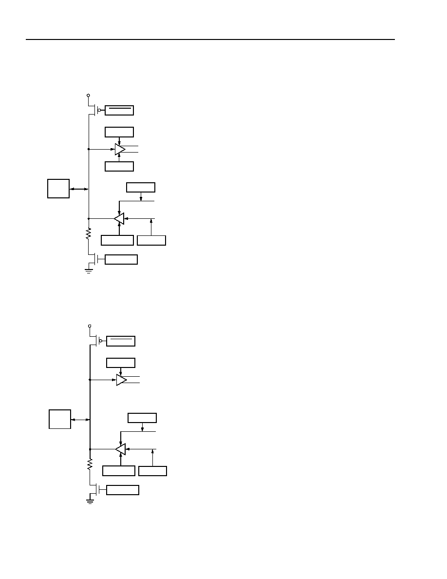
26
Lucent Technologies Inc.
Data Sheet
ORCA Series 2 FPGAs
June 1999
Programmable Input/Output Cells
(continued)
A. Simplified Diagram of OR2CxxA Programmable
I/O Cell (PIC)
B. Simplified Diagram of OR2TxxA/OR2TxxB
Programmable I/O Cell (PIC)
Figure 24. Simplified Diagrams
Outputs
The PIC's output drivers have programmable drive
capability and slew rates. Three propagation delays
(fast, slewlim, sinklim) are available on output drivers.
The sinklim mode has the longest propagation delay
and is used to minimize system noise and minimize
power consumption. The fast and slewlim modes allow
critical timing to be met.
The drive current is 12 mA sink/6 mA source for the
slewlim and fast output speed selections and
6 mA sink/3 mA source for the sinklim output. Two adja-
cent outputs can be interconnected to increase the out-
put sink current to 24 mA.
All outputs that are not speed critical should be config-
ured as sinklim to minimize power and noise. The num-
ber of outputs that switch simultaneously in the same
direction should be limited to minimize ground bounce.
To minimize ground bounce problems, locate heavily
loaded output buffers near the ground pads. Ground
bounce is generally a function of the driving circuits,
traces on the PCB, and loads and is best determined
with a circuit simulation.
Outputs can be inverted, and 3-state control signals
can be active-high or active-low. An open-drain output
may be obtained by using the same signal for driving
the output and 3-state signal nets so that the buffer out-
put is enabled only by a low. At powerup, the output
drivers are in slewlim mode, and the input buffers are
configured as TTL-level compatible with a pull-up. If an
output is not to be driven in the selected configuration
mode, it is 3-stated.
5 V Tolerant I/O (OR2TxxA)
The I/O on the OR2TxxA series devices allow intercon-
nection to both 3.3 V and 5 V device (selectable on a
per-pin basis) by way of special V
DD
5 pins that have
been added to the OR2TxxA devices. If any I/O on the
OR2TxxA device interfaces to a 5 V input, then all of
the V
DD
5 pins must be connected to the 5 V supply. If
no pins on the device interface to a 5 V signal, then the
V
DD
5 pins must be connected to the 3.3 V supply.
If the V
DD
5 pins are disconnected (i.e., they are float-
ing), the device will not be damaged; however, the
device may not operate properly until V
DD
5 is returned
to a proper voltage level. If the V
DD
5 pins are then
shorted to ground, a large current flow will develop, and
the device may be damaged.
PULL-UP
V
DD
DELAY
TTL/CMOS
PAD
SLEW RATE
POLARITY
DOUT/OUT
PULL-DOWN
dintb, dinlr
in
POLARITY
TRI
5-4591(F)
PULL-UP
V
DD
DELAY
PAD
SLEW RATE
POLARITY
DOUT/OUT
PULL-DOWN
dintb, dinlr
in
POLARITY
TRI
5-4591.T(F)

Lucent Technologies Inc.
27
Data Sheet
June 1999
ORCA Series 2 FPGAs
Programmable Input/Output Cells
(continued)
Regardless of the power supply that the V
DD
5 pins are
connected to (5 V or 3.3 V), the OR2TxxA devices will
drive the pin to the 3.3 V levels when the output buffer
is enabled. If the other device being driven by the
OR2TxxA device has TTL-compatible inputs, then the
device will not dissipate much input buffer power. This
is because the OR2TxxA output is being driven to a
higher level than the TTL level required. If the other
device has a CMOS-compatible input, the amount of
input buffer power will also be small. Both of these
power values are dependent upon the input buffer char-
acteristics of the other device when driven at the
OR2TxxA output buffer voltage levels.
The 2TxxA device has internal programmable pull-ups
on the I/O buffers. These pull-up voltages are always
referenced to V
DD
. This means that the V
DD
5 voltage
has no effect on the value of the pull-up voltage at the
pad. This voltage level is always sufficient to pull the
input buffer of the 2TxxA device to a high state. The pin
on the 2TxxA device will be at a level 1.0 V below V
DD
(minimum of 2.0 V with a minimum V
DD
of 3.0 V). This
voltage is sufficient to pull the external pin up to a 3.3 V
CMOS high-input level (1.8 V min) or a TTL high-input
level (2.0 V min) in a 5 V tolerant system, but it will
never pull the pad up to the V
DD
5 rail. Therefore, in a
5 V tolerant system using 5 V CMOS parts, care must
be taken to evaluate the use of these pull-ups to pull
the pin of the 2TxxA device to a typical 5 V CMOS
high-input level (2.2 V min).
For more information on 5 V tolerant I/Os, please see
ORCA
Æ
Series 5 V Tolerant I/Os
Application Note
(AP99-027FPGA), May 1999.
5 V Tolerant I/O (OR2TxxB)
The I/O on the OR2TxxB Series devices allow intercon-
nection to both 3.3 V and 5 V device (selectable on a
per-pin basis). Unlike the OR2TxxA family, when inter-
faceing into a 5 V signal, it no longer requires a V
DD
5
supply.
The OR2TxxB devices will drive the pin to the 3.3 V lev-
els when the output buffer is enabled. If the other
device being driven by the OR2TxxB device has TTL-
compatible inputs, then the device will not dissipate
much input buffer power. This is because the OR2TxxB
output is being driven to a higher level than the TTL
level required. If the other device has a CMOS-compat-
ible input, the amount of input buffer power will also be
small. Both of these power values are dependent upon
the input buffer characteristics of the other device when
driven at the OR2TxxB output buffer voltage levels.
The OR2TxxB device has internal programmable pull-
ups on the I/O buffers. These pull-up voltages are
always referenced to V
DD
and are always sufficient to
pull the input buffer of the OR2TxxB device to a high
state. The pin on the OR2TxxB device will be at a level
1.0 V below V
DD
(minimum of 2.0 V with a minimum
V
DD
of 3.0 V). This voltage is sufficient to pull the exter-
nal pin up to a 3.3 V CMOS high-input level (1.8 V, min)
or a TTL high input level (2.0 V, min) in a 5 V tolerant
system. Therefore, in a 5 V tolerant system using 5 V
CMOS parts, care must be taken to evaluate the use of
these pull-ups to pull the pin of the OR2TxxB device to
a typical 5 V CMOS high-input level (2.2 V, min).
PCI Compliant I/O
The I/O on the OR2TxxB Series devices allows compli-
ance with PCI local bus (Rev. 2.1) 5 V and 3.3 V signal-
ing environments. The signaling environment used for
each input buffer can be selected on a per-pin basis.
The selection provides the appropriate I/O clamping
diodes for PCI compliance.
OR2TxxB devices have 5 V tolerant I/Os as previously
explained, but can optionally be selected on a pin-by-
pin basis to be PCI bus 3.3 V signaling compliant (PCI
bus 5 V signaling compliance occurs in 5 V tolerant
operation mode). Inputs may have a pull-up or pull-
down resistor selected on an input for signal stabiliza-
tion and power management. Input signals in a PIO
can be passed to PIC routing on any of three paths,
two general signal paths into PIC routing, and/or a fast
route into the clock routing system.
OR2TxxA series devices are only compliant in 3.3 V
PCI Local Bus (Rev 2.1) signalling environments.
OR2CxxA devices are only compliant in 5 V PCI Local
Bus (Rev 2.1) signalling environments.

28
Lucent Technologies Inc.
Data Sheet
ORCA Series 2 FPGAs
June 1999
Programmable Input/Output Cells
(continued)
PIC Routing Resources
The PIC routing is designed to route 4-bit wide buses
efficiently. For example, any four consecutive I/O pads
can have both their input and output signals routed into
one PLC. Using only PIC routing, either the input or
output data can be routed to/from a single PLC from/to
any eight pads in a row, as in Figure 25.
The connections between PLCs and the I/O pad are
provided by two basic types of routing resources.
These are routing resources internal to the PIC and
routing resources used for PIC-PLC connection.
Figure 26 and Figure 27 show a high-level and detailed
view of these routing resources, respectively.
5-4504(F)
Figure 25. Simplified PIC Routing Diagram
The PIC's name is represented by a two-letter designa-
tion to indicate on which side of the device it is located
followed by a number to indicate in which row or col-
umn it is located. The first letter, P, designates that the
cell is a PIC and not a PLC. The second letter indicates
the side of the array where the PIC is located. The four
sides are left (L), right (R), top (T), and bottom (B). The
individual I/O pad is indicated by a single letter (either
A, B, C, or D) placed at the end of the PIC name. As an
example, PL10A indicates a pad located on the left
side of the array in the tenth row.
Each PIC has four pads and each pad can be config-
ured as an input, an output (3-statable), a direct output,
or a bidirectional I/O. When the pads are used as
inputs, the external signals are provided to the internal
circuitry at IN[3:0]. When the pads are used to provide
direct inputs to the latches/FFs, they are connected
through DIN[3:0]. When the pads are used as outputs,
the internal signals connect to the pads through
OUT[3:0]. When the pads are used as direct outputs,
the output from the latches/flip-flops in the PLCs to the
PIC is designated DOUT[3:0]. When the outputs are
3-statable, the 3-state enable signals are TS[3:0].
Routing Resources Internal to the PIC
For inter-PIC routing, the PIC contains 14 lines used to
route signals around the perimeter of the FPGA. Figure
25 shows these lines running vertically for a PIC
located on the left side. Figure 26 shows the lines run-
ning horizontally for a PIC located at the top of the
FPGA.
PXL Lines. Each PIC has two PXL lines, labeled
PXL[1:0]. Like the XL lines of the PLC, the PXL lines
span the entire edge of the FPGA.
PXH Lines. Each PIC has four PXH lines, labeled
PXH[3:0]. Like the XH lines of the PLC, the PXH lines
span half the edge of the FPGA.
PX2 Lines. There are four PX2 lines in each PIC,
labeled PX2[3:0]. The PX2 lines pass through two adja-
cent PICs before being broken. These are used to
route nets around the perimeter equally a distance of
two or more PICs.
PX1 Lines. Each PIC has four PX1 lines, labeled
PX1[3:0]. The PX1 lines are one PIC long and are
extended to adjacent PICs by enabling CIPs.
PAD D
I/O3
4
PXL
2
CK
2
PIC
SWITCHING
MATRIX
PAD C
I/O2
4
PAD B
I/O1
4
PAD A
I/O0
4
PXH
4
PX2
4
PX1
4
PLC X4
4
PLC X1
4
PLC PSW
5
PLC DOUT
4
PLC XL
4
PLC XH
4
PLC X1
4
PLC X4
4
PLC DIN
4
PXL
2
PXH
4
PX2
4
PX1
4

Lucent Technologies Inc.
29
Data Sheet
June 1999
ORCA Series 2 FPGAs
Programmable Input/Output Cells
(continued)
PIC Architectural Description
The PIC architecture given in Figure 26 is described
using the following letter references. The figure depicts
a PIC at the top of the array, so inter-PIC routing is hor-
izontal and the indirect PIC-PLC routing is horizontal to
vertical. In some cases, letters are provided in more
than one location to indicate the path of a line.
A. As in the PLCs, the PIC contains a set of lines which
run the length (width) of the array. The PXL lines
connect in the corners of the array to other PXL
lines. The PXL lines also connect to the PIC BIDI,
PIC BIDIH, and LLDRV lines. As in the PLC XL lines,
the PXH lines twist as they propagate through the
PICs.
B. As in the PLCs, the PIC contains a set of lines which
run one-half the length (width) of the array. The PXH
lines connect in the corners and in the middle of the
array perimeter to other PXH lines. The PXH lines
also connect to the PIC BIDI, PIC BIDIH, and
LLDRV lines. As in the PLC XH lines, the PXH lines
do not twist as they propagate through the PICs.
C. The PX2[3:0] lines span a length of two PICs before
intersecting with a CIP. The CIP allows the length of
a path using PX2 lines to be extended two PICs.
D. The PX1[3:0] lines span a single PIC before inter-
secting with a CIP. The CIP allows the length of a
path using PX1 lines to be extended by one PIC.
E. These are four dedicated direct output lines con-
nected to the output buffers. The DOUT[3:0] signals
go directly from a PLC latch/FF to an output buffer,
minimizing the latch/FF to pad propagation delay.
F. This is a direct path from the input pad to the PLC
latch/flip-flops in the two rows (columns) adjacent to
PICs. This input allows a reduced setup time. Direct
inputs from the top and bottom PIC rows are
PDINTB[3:0]. Direct inputs from the left and right
PIC columns are PDINLR[3:0].
G. The OUT[3:0], TS[3:0], and IN[3:0] signals for each
I/O pad can be routed directly to the adjacent PLC's
switching lines.
H. The four TRIDI buffers allow connections from the
pads to the PLC XL lines. The TRIDIs also allow
connections between the PLC XL lines and the
PBIDI lines, which are described in J below.
I. The four TRIDIH buffers allow connections from the
pads to the PLC XH lines. The TRIDIHs also allow
connections between the PLC XH lines and the
pBIDIH lines, which are described in K below.
J. The PBIDI lines (bidi[3:0]) connect the PXL lines,
PXH lines, and the PX1 lines. These are bidirec-
tional in that the path can be from the PXL, PXH, or
PX1 lines to the XL lines, or from the XL lines to the
PXL, PXH, or PX1 lines.
K. The pBIDIH lines (BIDIH[3:0]) connect the PXL
lines, PXH lines, and the PX1 lines. These are bidi-
rectional in that the path can be from the PXL, PXH,
or PX1 lines to the XH lines, or from the XH lines to
the PXL, PXH, or PX1 lines.
L. The LLIN[3:0] lines provide a fast connection from
the I/O pads to the XL and XH lines.
M.This set of CIPs allows the eight X1 lines (four on
each side) of the PLC perpendicular to the PIC to be
connected to either the PX1 or PX2 lines in the PIC.
N. This set of CIPs allows the eight X4 lines (four on
each side) of the PLC perpendicular to the PIC to be
connected to the PX1 lines. This allows fast access
to/from the I/O pads from/to the PLCs.
O. All four of the PLC X4 lines in a group connect to all
four of the PLC X4 lines in the adjacent PLC through
a CIP. (This differs from the
ORCA
1C
Series in
which two of the X4 lines in adjacent PLCs are
directly connected without any CIPs.)
P. The long-line driver (LLDRV) line can be driven by
the XSW4 switching line of the adjacent PLC. To pro-
vide connectivity to the pads, the LLDRV line can
also connect to any of the four PXH or to one of the
PXL lines. The 3-state enable (TS[i]) for all four I/O
pads can be driven by XSW4, PXH, or PXL lines.
Q. For fast clock routing, one of the four I/O pads in
each PIC can be selected to be driven onto a dedi-
cated clock line. The clock line spans the length
(width) of the PLC array. This dedicated clock line is
typically used as a clock spine. In the PLCs, the
spine is connected to an XL line to provide a clock
branch in the perpendicular direction. Since there is
another clock line in the PIC on the opposite side of
the array, only one of the I/O pads in a given row
(column) can be used to generate a global signal in
this manner, if all PLCs are driven by the signal.

Data Sheet
ORCA Series 2 FPGAs
June 1999
30
Lucent Technologies Inc.
Programmable Input/Output Cells
(continued)
5-2843(F).r8
Figure 26. PIC Architecture
D T
D T
D T
D T
PA
PB
PC
PD
PXL[1]
PXL[0]
PX2[2]
PX2[3]
PX2[0]
PX2[1]
PX1[0]
PX1[1]
PX1[2]
PX1[3]
PXH[1]
PXH[2]
PXH[3]
PXH[0]
B
A
C
D
F
E
G
Q
PXL[0]
PXL[1]
PX2[0]
PX2[1]
PX2[2]
PX2[3]
PX1[0]
PX1[1]
PX1[2]
PX1[3]
PXH[1]
PXH[2]
PXH[3]
PXH[0]
B
A
C
D
TS
0
OU
T0
IN
0
DO
UT
0
TS
1
OU
T1
IN
1
DO
UT
1
TS
3
OU
T3
IN
3
DO
UT
3
TS
2
OU
T2
IN
2
DO
UT
2
PIC DETAIL
BI
D
I
3
F
O
N
O
LLDRV
M
I
L
J
K
N
D
C
P
Q
M
B
I
DIH3
B
I
DIH2
B
I
DIH1
B
I
DIH0
BI
D
I
2
BI
D
I
1
BI
D
I
0
LL
I
N
3
LL
I
N
2
LL
I
N
1
LL
I
N
0
P
P
VX
L
[
3
]
VX
L
[
2
]
VX
L
[
1
]
VX
L
[
0
]
VX
1
[
7
]
VX
1
[
6
]
VX
1
[
5
]
VX
1
[
4
]
VX
1
[
3
]
VX
1
[
2
]
VX
1
[
1
]
VX
1
[
0
]
DO
UT
[
3
]
DO
UT
[
2
]
DO
UT
[
1
]
XS
W
[
3
]
XS
W
[
2
]
XS
W
[
1
]
XS
W
[
0
]
XS
W
[
4
]
DO
UT
[
0
]
CK
T
VXH
[
3
]
VXH
[
2
]
VXH
[
1
]
VXH
[
0
]
VX
4
[
7
]
VX
4
[
6
]
VX
4
[
5
]
VX
4
[
4
]
P
D
IN
T
B
[3
]
P
D
IN
T
B
[2
]
P
D
IN
T
B
[1
]
P
D
IN
T
B
[0
]
VX
4
[
3
]
VX
4
[
2
]
VX
4
[
1
]
VX
4
[
0
]
PLC-PIC Routing Resources
There is no direct connection between the inter-PIC
lines and the PLC lines. All connections to/from the
PLC must be done through the connecting lines which
are perpendicular to the lines in the PIC. The use of
perpendicular and parallel lines will be clearer if the
PLC and PIC architectures (Figure 23 and Figure 26)
are placed side by side. Twenty-nine lines in the PLC
can be connected to the 15 lines in the PIC.
Multiple connections between the PIC PX1 lines and
the PLC X1 lines are available. These allow buses
placed in any arbitrary order on the I/O pads to be
unscrambled when placed on the PLC X1 lines. Con-
nections are also available between the PIC PX2 lines
and the PLC X1 lines.
There are eight tridirectional (four TRIDI/four TRIDIH)
buffers in each PIC; they can do the following:
s
Drive a signal from an I/O pad onto one of the adja-
cent PLC's XL or XH lines
s
Drive a signal from an I/O pad onto one of the two
PXL or four PXH lines in the PIC
s
Drive a signal from the PLC XL or XH lines onto one
of the two PXL or four PXH lines in the PIC
s
Drive a signal from the PIC PXL or PXH lines onto
one of the PLC XL or XH lines

Data Sheet
June 1999
ORCA Series 2 FPGAs
Lucent Technologies Inc.
31
Programmable Input/Output Cells
(continued)
Figure 27 shows paths to and from pads and the use of MUX CIPs to connect lines. Detail A shows six MUX CIPs
for the pad P0 used to construct the net for the 3-state signal. In the MUX CIP, one of six lines is connected to a line
to form the net. In this case, the ts0 signal can be driven by either of the two PXLs, PX1[0], PX1[1], XSW[0], or the
LLDRV lines. Detail B shows the four MUX CIPs used to drive the P1 output. The source line for OUT1 is either
XSW[1], PX1[1], PX1[3], or PX2[2].
5-2843.BL(F).2C.r3
Figure 27. PIC Detail
D T
D T
D T
D T
PA
PB
PC
PD
TS
0
OUT0
IN0
DOUT0
TS
1
OUT1
IN1
DOUT1
TS
3
OUT3
IN3
DOUT3
TS
2
OUT2
IN2
DOUT2
PXL[1]
PXL[0]
PX2[2]
PX2[3]
PX2[0]
PX2[1]
PX1[0]
PX1[1]
PX1[2]
PX1[3]
PXH[1]
PXH[2]
PXH[3]
PXH[0]
PXL[1]
PXL[0]
PX2[2]
PX2[3]
PX2[0]
PX2[1]
PX1[0]
PX1[1]
PX1[2]
PX1[3]
PXH[1]
PXH[2]
PXH[3]
PXH[0]
DOUT[0]
DOUT[1]
DOUT[2]
DOUT[3]
XSW[0]
XSW[1]
XSW[2]
XSW[3]
LLDRV
A
B
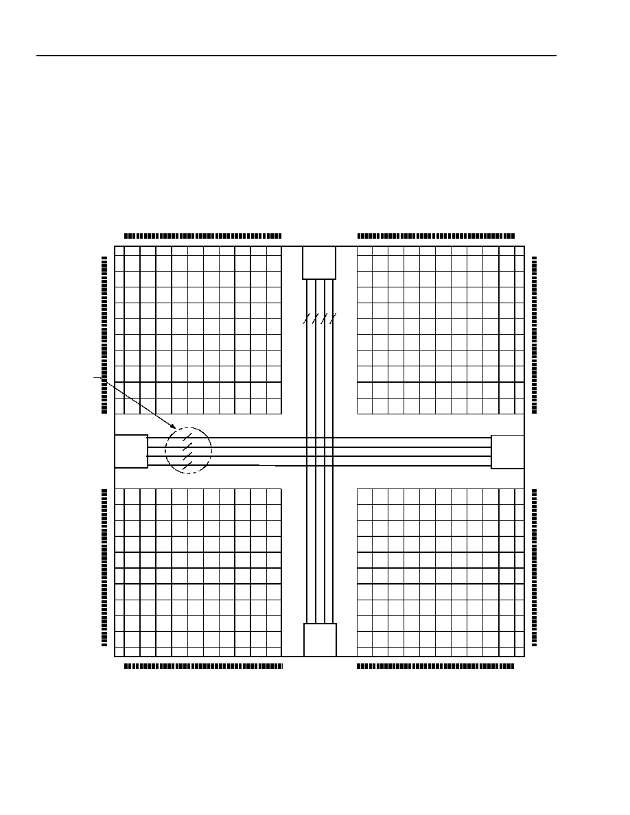
Data Sheet
ORCA Series 2 FPGAs
June 1999
32
Lucent Technologies Inc.
Interquad Routing
In all the
ORCA
Series 2 devices, the PLC array is split
into four equal quadrants. In between these quadrants,
routing has been added to route signals between the
quadrants, especially to the quadrant in the opposite
corner. The two types of interquad blocks, vertical and
horizontal, are pitch matched to PICs. Vertical inter-
quad blocks (vIQ) run between quadrants on the left
and right, while horizontal interquad blocks (hIQ) run
between top and bottom quadrants. Since hIQ and vIQ
blocks have the same logic, only the hIQ block is
described below.
The interquad routing connects XL and XH lines. It
does not affect local routing (XSW, X1, X4, fast carry),
so local routing is the same, whether PLC-PLC con-
nections cross quadrants or not. There are no connec-
tions to the local lines in the interquad blocks. Figure 28
presents a (not to scale) view of interquad routing.
Figure 28. Interquad Routing
5-4538(F)
vIQ0[4:
0
]
vIQ1[4:0
]
vIQ2[4:
0
]
vIQ3[4:0
]
5
5
5
5
TMID
BMID
hIQ3[4:0]
hIQ2[4:0]
hIQ1[4:0]
hIQ0[4:0]
5
5
5
5
SEE
DETAIL IN
FIGURE 29
RMID
LMID

Data Sheet
June 1999
ORCA Series 2 FPGAs
Lucent Technologies Inc.
33
Interquad Routing
(continued)
In the hIQ block in Figure 29, the XH lines from one
quadrant connect through a CIP to its counterpart in
the opposite quadrant, creating a path that spans the
PLC array. Since a passive CIP is used to connect the
two XH lines, a 3-state signal can be routed on the two
XH lines in the opposite quadrants, and then they can
be connected through this CIP.
In the hIQ block, the 20 hIQ lines span the array in a
horizontal direction. The 20 hIQ lines consist of four
groups of five lines each. To effectively route nibble-
wide buses, each of these sets of five lines can connect
to only one of the bits of the nibble for both the XH and
XL. For example, hIQ0 lines can only connect to the
XH0 and XL0 lines, and the hIQ1 lines can connect
only to the XH1 and XL1 lines, etc. Buffers are provided
for routing signals from the XH and XL lines onto the
hIQ lines and from the hIQ lines onto the XH and XL
lines. Therefore, a connection from one quadrant to
another can be made using only two XH lines (one in
each quadrant) and one interquad line.
5-4537(F).r3
Figure 29. hIQ Block Detail
hIQ3[4]
hIQ3[3]
hIQ3[2]
hIQ3[1]
hIQ3[0]
hIQ2[4]
hIQ2[3]
hIQ2[2]
hIQ2[1]
hIQ2[0]
hIQ1[4]
hIQ1[3]
hIQ1[2]
hIQ1[1]
hIQ1[0]
hIQ0[4]
hIQ0[3]
hIQ0[2]
hIQ0[1]
hIQ0[0]
VXH[
3
]
VXH[
2
]
VXH[
1
]
VXH[
0
]
VXL
[
3
]
VXL
[
2
]
VXL
[
1
]
VXL
[
0
]
VX4
[
7
]
VX4
[
6
]
VX4
[
5
]
VX4
[
4
]
VX1
[
7
]
VX1
[
6
]
VX1
[
5
]
VX1
[
4
]
VX
4
[
7
]
VX
4
[
6
]
VX
4
[
5
]
VX
4
[
4
]
VX
1
[
7
]
VX
1
[
6
]
VX
1
[
5
]
VX
1
[
4
]
VX
H
[
3
]
VX
H
[
2
]
VX
H
[
1
]
VX
H
[
0
]
VX
L
[
3
]
VX
L
[
2
]
VX
L
[
1
]
VX
L
[
0
]
hIQ3[4]
hIQ3[3]
hIQ3[2]
hIQ3[1]
hIQ3[0]
hIQ2[4]
hIQ2[3]
hIQ2[2]
hIQ2[1]
hIQ2[0]
hIQ1[4]
hIQ1[3]
hIQ1[2]
hIQ1[1]
hIQ1[0]
hIQ0[4]
hIQ0[3]
hIQ0[2]
hIQ0[1]
hIQ0[0]
CA
RR
Y
CARR
Y
VX4
[
3
]
VX4
[
2
]
VX4
[
1
]
VX4
[
0
]
VX1
[
3
]
VX1
[
2
]
VX1
[
1
]
VX1
[
0
]
VX
1
[
3
]
VX
1
[
2
]
VX
1
[
1
]
VX
1
[
0
]
VX
4
[
3
]
VX
4
[
2
]
VX
4
[
1
]
VX
4
[
0
]
IN
T
[
4
]
IN
T
[
3
]
IN
T
[
2
]
IN
T
[
1
]
IN
T
[
0
]
GS
R
N
CK
B
CK
T
INB
[
4]
INB
[
3]
INB
[
2]
INB
[
1]
INB
[
0]
GS
R
N
CK
B
CK
T

Data Sheet
ORCA Series 2 FPGAs
June 1999
34
Lucent Technologies Inc.
Interquad Routing
(continued)
Subquad Routing (OR2C40A/OR2T40A Only)
In the
ORCA
OR2C40A/OR2T40A/OR2T40B, each
quadrant of the device is split into smaller arrays of
PLCs called subquads. Each of these subquads is
made of a 4 x 4 array of PLCs (for a total of 16 per sub-
quadrant), except at the outer edges of array, which
have less than 16 PLCs per subquad. New routing
resources, called subquad lines, have been added
between each adjacent pair of subquads to enhance
the routability of the device. A portion of the center of
the OR2C40A and OR2T40A array is shown in Figure
30, including the subquad blocks containing a 4 x 4
array of PLCs, the interquad routing lines, and the sub-
quad routing lines.
All of the inter-PLC routing resources discussed previ-
ously continue to be routed between a PLC and its
adjacent PLC, even if the two adjacent PLCs are in dif-
ferent subquad blocks. Since the PLC routing has not
been modified for the OR2C40A/OR2T40A architec-
tures, this means that all of the same routing connec-
tions are possible for these devices as for any other
ORCA
2C series device. In this way, both the
OR2C40A and OR2T40A/OR2T40B are upwardly com-
patible when compared with the ATT2Cxx series
devices. As the inter-PLC routing runs between sub-
quad blocks, it crosses the new subquad lines. When
this happens, CIPs are used to connect the subquad
lines to the X4 and/or the XH lines which lie along the
other axis of the PLC array.
5-4200(F).r5
Figure 30. Subquad Blocks and Subquad Routing
SUBQUAD
(4 x 4 PLCs)
SUBQUAD
(4 x 4 PLCs)
SUBQUAD
(4 x 4 PLCs)
SUBQUAD
(4 x 4 PLCs)
SUBQUAD
(4 x 4 PLCs)
SUBQUAD
(4 x 4 PLCs)
SUBQUAD
(4 x 4 PLCs)
SUBQUAD
(4 x 4 PLCs)
SUBQUAD
(4 x 4 PLCs)
SUBQUAD
(4 x 4 PLCs)
SUBQUAD
(4 x 4 PLCs)
SUBQUAD
(4 x 4 PLCs)
SUBQUAD
(4 x 4 PLCs)
SUBQUAD
(4 x 4 PLCs)
SUBQUAD
(4 x 4 PLCs)
SUBQUAD
(4 x 4 PLCs)
SEE DETAIL
IN FIGURES 25
AND 26
HORIZONTAL
INTERQUAD
ROUTING
(hIQ)
HORIZONTAL
SUBQUAD
ROUTING
(HSUB)
VERTICAL
SUBQUAD
ROUTING
(VSUB)
VERTICAL
INTERQUAD
ROUTING
(vIQ)

Lucent Technologies Inc.
35
Data Sheet
June 1999
ORCA Series 2 FPGAs
Interquad Routing
(continued)
5-4201(F).r4
Figure 31. Horizontal Subquad Routing
Connectivity
The X4 and XH lines make the only connections to the
subquad lines; therefore, the array remains symmetri-
cal and homogeneous. Since each subquad is made
from a 4 x 4 array of PLCs, the distance between sets
of subquad lines is four PLCs, which is also the dis-
tance between the breaks of the X4 lines. Therefore,
each X4 line will cross exactly one set of subquad lines.
Since all X4 lines make the same connections to the
subquad lines that they cross, all X4 lines in the array
have the same connectivity, and the symmetry of the
routing is preserved. Since all XH lines cross the same
number of subquad blocks, the symmetry is maintained
for the XH lines as well.
The new subquad lines travel a length of eight PLCs
(seven PLCs on the outside edge) before they are bro-
ken. Unlike other inter-PLC lines, they cannot be con-
nected end-to-end. As shown in Figure 30, some of the
horizontal (vertical) subquad lines have connectivity to
the subquad to the left of (above) the current subquad,
while others have connectivity to the subquad to the
right (below). This allows connections to/from the cur-
rent subquad from/to the PLCs in all subquads that sur-
round it.
Between all subquads, including in the center of the
array, there are three groups of subquad lines where
each group contains four lines. Figure 31 shows the
connectivity of these three groups of subquad lines
(HSUB) to the VX4 and VXH lines running between a
vertical pair of PLCs. Between each vertical pair of
subquad blocks, four of the blocks shown in Figure 31
are used, one for each pair of vertical PLCs.
The first two groups, depicted as A and B, have con-
nectivity to only one of the two sets of X4 lines between
pairs of PLCs. Since they are very lightly loaded, they
are very fast. The third group, C, connects to both
groups of X4 lines between pairs of PLCs, as well as all
of the XH lines between pairs of PLCs, providing high
flexibility. The connectivity for the vertical subquad rout-
ing (Vsub) is the same as described above for the hori-
zontal subquad routing, when rotated onto the other
axis.
At the center row and column of each quadrant, a
fourth group of subquad lines has been added. These
subquad lines only have connectivity to the XH lines.
The XH lines are also broken at this point, which
means that each XH line travels one-half of the quad-
rant (i.e., one-quarter of the device) before it is broken
by a CIP. Since the XH lines can be connected end-to-
end, the resulting line can be either one-quarter, one-
half, three-quarters, or the entire length of the array.
The connectivity of the XH lines and this fourth group of
subquad lines, indicated as D, are detailed in Figure
32. Again, the connectivity for the vertical subquad
routing (VSUB) is the same as the horizontal subquad
routing, when rotated onto the other axis.
5-4202(F).r3
Figure 32. Horizontal Subquad Routing
Connectivity (Half Quad)
A
C
B
HSUB[11]
HSUB[10]
HSUB[9]
HSUB[8]
HSUB[7]
HSUB[6]
HSUB[5]
HSUB[4]
HSUB[3]
HSUB[2]
HSUB[1]
HSUB[0]
HSUB[11]
HSUB[10]
HSUB[9]
HSUB[8]
HSUB[7]
HSUB[6]
HSUB[5]
HSUB[4]
HSUB[3]
HSUB[2]
HSUB[1]
HSUB[0]
VX4[7]
VX4[6]
VX4[5]
VX4[4]
VX4[3]
VX4[2]
VX4[1]
VX4[0]
VX4[3]
VX4[2]
VX4[1]
VX4[0]
VX4[7]
VX4[6]
VX4[5]
VX4[4]
VX4[3]
VX4[2]
VX4[1]
VX4[0]
VX4[3]
VX4[2]
VX4[1]
VX4[0]
A
D
B
HSUB[11]
HSUB[10]
HSUB[9]
HSUB[8]
HSUB[15]
HSUB[14]
HSUB[13]
HSUB[12]
HSUB[3]
HSUB[2]
HSUB[1]
HSUB[0]
HSUB[11]
HSUB[10]
HSUB[9]
HSUB[8]
HSUB[15]
HSUB[14]
HSUB[13]
HSUB[12]
HSUB[3]
HSUB[2]
HSUB[1]
HSUB[0]
VX
4
[
7
]
VX
4
[
6
]
VX
4
[
5
]
VX
4
[
4
]
VX
4
[
3
]
VX
4[
2
]
VX
4
[
1
]
VX
4
[
0
]
VX
4
[
3
]
VX
4
[
2
]
VX
4
[
1
]
VX
4
[
0
]
VX
4
[
7
]
VX
4
[
6
]
VX
4
[
5
]
VX
4
[
4
]
VX
4
[
3
]
VX
4
[
2
]
VX
4
[
1
]
VX
4
[
0
]
VX
4
[
3
]
VX
4
[
2
]
VX
4
[
1
]
VX
4
[
0
]
C
HSUB[7]
HSUB[6]
HSUB[5]
HSUB[4]
HSUB[7]
HSUB[6]
HSUB[5]
HSUB[4]
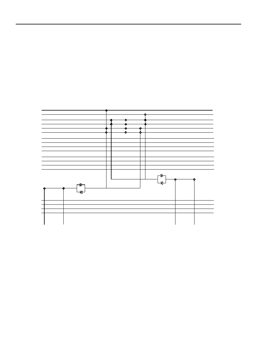
Data Sheet
ORCA Series 2 FPGAs
June 1999
36
Lucent Technologies Inc.
Interquad Routing
(continued)
PIC Interquad (MID) Routing
Between the PICs in each quadrant, there is also con-
nectivity between the PIC routing and the interquad
routing. These blocks are called LMID (left), TMID
(top), RMID (right), and BMID (bottom). The TMID rout-
ing is shown in Figure 33. As with the hIQ and vIQ
blocks, the only connectivity to the PIC routing is to the
global PXH and PXL lines.
The PXH lines from the one quadrant can be con-
nected through a CIP to its counterpart in the opposite
quadrant, providing a path that spans the array of PICs.
Since a passive CIP is used to connect the two PXH
lines, a 3-state signal can be routed on the two PXH
lines in the opposite quadrants, and then connected
through this CIP. As with the hIQ and vIQ blocks, CIPs
and buffers allow nibble-wide connections between the
interquad lines, the XH lines, and the XL lines.
5-4201(F).r4
Figure 33. Top (TMID) Routing
PXL[1]
PXL[0]
PX4[3]
PX4[2]
PX4[1]
PX4[0]
PX1[3]
PX1[2]
PX1[1]
PX1[0]
V
IQ0
[0]
PXH[2]
PXH[1]
PXH[0]
HX4[3]
HX4[2]
HX4[1]
HX4[0]
V
IQ1
[0]
VI
Q
2
[
0
]
VI
Q
3
[
0
]
PXH[3]
PXL[1]
PXL[0]
PX4[3]
PX4[2]
PX4[1]
PX4[0]
PX1[3]
PX1[2]
PX1[1]
PX1[0]
PXH[2]
PXH[1]
PXH[0]
HX4[3]
HX4[2]
HX4[1]
HX4[0]
PXH[3]

Lucent Technologies Inc.
37
Data Sheet
June 1999
ORCA Series 2 FPGAs
Programmable Corner Cells
Programmable Routing
The programmable corner cell (PCC) contains the cir-
cuitry to connect the routing of the two PICs in each
corner of the device. The PIC PX1 and PX2 lines are
directly connected together from one PIC to another.
The PIC PXL lines are connected from one block to
another through tridirectional buffers. Four CIPs in
each corner connect the four PXH lines from each side
of the device.
Special-Purpose Functions
In addition to routing functions, special-purpose func-
tions are located in each FPGA corner. The upper-left
PCC contains connections to the boundary-scan logic.
The upper-right PCC contains connections to the read-
back logic and the connectivity to the global 3-state
signal (TS_ALL). The lower-left PCC contains connec-
tions to the internal oscillator.
The lower-right PCC contains connections to the start-
up and global reset logic. During configuration, the
RESET
input pad always initiates a configuration abort,
as described in the FPGA States of Operation section.
After configuration, the global set/reset signal (GSRN)
can either be disabled (the default), directly connected
to the
RESET
input pad, or sourced by a lower-right
corner signal. If the
RESET
input pad is not used as a
global reset after configuration, this pad can be used as
a normal input pad. During start-up, the release of the
global set/reset, the release of the I/Os, and the
release of the external DONE signal can each be timed
individually based upon the start-up clock. The start-up
clock can come from CCLK or it can be routed into the
start-up block using the lower-right corner routing
resources. More details on start-up can be found in the
FPGA States of Operation section.
Clock Distribution Network
The
ORCA
Series 2 clock distribution schemes use pri-
mary and secondary clocks. This provides the system
designer with additional flexibility in assigning clock
input pins.
One advantage is that board-level clock traces routed
to the FPGA are shorter. On a PC board, the added
length of high-speed clock traces routed to dedicated
clock input pins can significantly increase the parasitic
impedances. The primary advantage of the
ORCA
clock distribution is the availability of a large number of
clocks, since all I/O pins are configurable as clocks.
Primary Clock
The primary clock distribution is shown in Figure 34. If
the clock signal is from an I/O pad, it can be driven onto
a clock line. The clock lines do not provide clock signals
directly to the PFU; they act as clock spines from which
clocks are branched to XL lines. The XL lines then feed
the clocks to PFUs. A multiplexer in each PLC is used
to transition from the clock spine to the branch.
For a clock spine in the horizontal direction, the inputs
into the multiplexer are the two lines from the left and
right PICs (CKL and CKR) and the local clock line from
the perpendicular direction (HCK). This signal is then
buffered and driven onto one of the vertical XL lines,
forming the branches. The same structure is used for a
clock spine in the vertical direction. In this case, the
multiplexer selects from lines from the top and bottom
PICs (CKT, CKB, and VCK) and drives the signal onto
one of the horizontal XL lines.
Figure 34 illustrates the distribution of the low-skew pri-
mary clock to a large number of loads using a main
spine and branches. Each row (column) has two dedi-
cated clock lines originating from PICs on opposite
sides of the array. The clock is input from the pads to
the dedicated clock line CKT to form the clock spine
(see Figure 34, Detail A). From the clock spine, net
branches are routed using horizontal XL lines and then
PLC clock inputs are tapped from the XL lines, as
shown in Figure 34, Detail B.
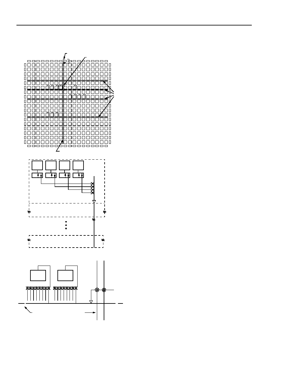
38
Lucent Technologies Inc.
Data Sheet
ORCA Series 2 FPGAs
June 1999
Clock Distribution Network
(continued)
5-4480(F).r3
Figure 34. Primary Clock Distribution
Secondary Clock
There are times when a primary clock is either not
available or not desired, and a secondary clock is
needed. For example:
s
Only one input pad per PIC can be placed on the
clock routing. If a second input pad in a given PIC
requires global signal routing, a secondary clock
route must be used.
s
Since there is only one branch driver in each PLC for
either direction (vertical and horizontal), both clock
lines in a particular row or column (CKL and CKR, for
example) cannot drive a branch. Therefore, two
clocks should not be placed into I/O pads in PICs on
the opposite sides of the same row or column if glo-
bal clocks are to be used.
s
Since the clock lines can only be driven from input
pads, internally generated clocks should use second-
ary clock routing.
Figure 35 illustrates the secondary clock distribution. If
the clock signal originates from either the left or right
side of the FPGA, it can be routed through the TRIDI
buffers in the PIC onto one of the adjacent PLC's hori-
zontal XL lines. If the clock signal originates from the
top or bottom of the FPGA, the vertical XL lines are
used for routing. In either case, an XL line is used as
the clock spine. In the same manner, if a clock is only
going to be used in one quadrant, the XH lines can be
used as a clock spine. The routing of the clock spine
from the input pads to the VXL (VXH) using the BIDIs
(BIDIHs) is shown in Figure 35, Detail A.
In each PLC, a low-skew connection through a long-
line driver can be used to connect a horizontal XL line
to a vertical XL line or vice versa. As shown in Figure
35, Detail B, this is used to route the branches from the
clock spine. If the clock spine is a vertical XL line, then
the branches are horizontal XL lines and vice versa.
The clock is then routed into each PLC from the XL line
clock branches.
To minimize skew, the PLC clock input for all PLCs
must be connected to the branch XL lines, not the
spine XL line. Even in PLCs where the clock is routed
from the spine to the branches, the clock should be
routed back into the PLC from the clock branch.
If the clock is to drive only a limited number of loads,
the PFUs can be connected directly to the clock spine.
In this case, all flip-flops driven by the clock must be
located in the same row or column.
CKT
CKB
HXL
HCK
R7C8
HCK
DETAIL B
R7C7
HXL
CLOCK
BRANCH
CLOCK
SPINES
PLC R1C8
PLC R18C8
PIC PT8
CLOCK SPINE
CKT
DETAIL A
A
B
C
D
CLOCK
CLOCK SPINE
SEE DETAIL A
SEE DETAIL B
CLK PIN
BRANCHES
D T
D T
D T
D T

Lucent Technologies Inc.
39
Data Sheet
June 1999
ORCA Series 2 FPGAs
Clock Distribution Network
(continued)
Alternatively, the clock can be routed from the spine to
the branches by using the BIDIs instead of the long-line
drivers. This results in added delay in the clock net, but
the clock skew is approximately equal to the clock
routed using the long-line drivers. This method can be
used to create a clock that is used in only one quad-
rant. The XH lines act as a clock spine, which is then
routed to perpendicular XH lines (the branches) using
the BIDIHs.
Clock signals, such as the output of a counter, can also
be generated in PLCs and routed onto an XL line,
which then acts as a clock spine. Although the clock
can be generated in any PLC, it is recommended that
the clock be located as close to the center of the FPGA
as possible to minimize clock skew.
Selecting Clock Input Pins
Any user I/O pin on an
ORCA
FPGA can be used as a
very fast, low-skew clock input. Choosing the first clock
pin is completely arbitrary, but using a pin that is near
the center of an edge of the device (as shown in Fig-
ures 34 and 35) will provide the lowest skew clock net-
work. The pin-to-pin timing numbers in the Timing
Characteristics section of this data book assume that
the clock pin is in one of the four PICs at the center of
any side of the device.
Once the first clock pin has been chosen, there are
only two sets of pins (within the center four PICs on
each side of the device) that should not be chosen as
the second clock pin: a pin from the same PIC, and/or a
pin from the PIC on the exact opposite edge of the die
(i.e., if a pin from a PIC on the top edge is chosen for
the first clock, the same PIC on the bottom edge should
not be chosen for the second clock).
These rules should be followed iteratively until a total of
eight clocks (or other global signals) have been
selected: four from the left/right sides of the device, and
four from the top/bottom sides of the device. If more
than eight clocks are needed, then select another pin
outside the center four PICs to use primary-clock rout-
ing, use secondary clock routing for any pin, or use
local clock routing.
If it is desired to use a pin for one of the first eight
clocks that is not within the center four PICs of any side
of the device and primary clock routing is desired, the
pad names (see Pin Information) of the two clock pins
on the top or bottom of the device cannot be a multi-
plier of four PICs away. The same rule applies to clock
pins on the left or right side of the device.
The following equation can be used to determine pin
names:
Pad number = P[RL][TB]n ± (i x 4)[A ≠ D]
Where i = 1--8, and n is the current PIC number.
For more information, please refer to
Utilizing the
ORCA
Æ
OR2C/TxxA Clock Distribution Network
Appli-
cation Note (AP97-055FPGA).
5-4481(F).r2
Figure 35. Secondary Clock Distribution
DT
DT
DT
DT
CLOCK
CLOCK SPINE
SEE DETAIL A
SEE DETAIL B
CLK PIN
BRANCHES
PFU
HCK
VCK
DETAIL B
PA
PB
VXL[3]
VXL[2]
VXL[1]
VXL[0]
VXH[3]
VXH[2]
VXH[1]
VXH[0]
DETAIL A
PC
PD
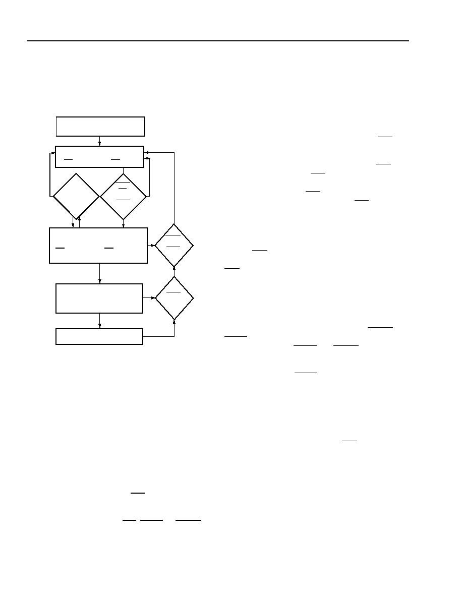
40
Lucent Technologies Inc.
Data Sheet
ORCA Series 2 FPGAs
June 1999
FPGA States of Operation
Prior to becoming operational, the FPGA goes through a
sequence of states, including initialization, configuration,
and start-up. Figure 36 outlines these three FPGA
states.
5-4529(F).r6
Figure 36. FPGA States of Operation
Initialization
Upon powerup, the device goes through an initialization
process. First, an internal power-on-reset circuit is trig-
gered when power is applied. When V
DD
reaches the
voltage at which portions of the FPGA begin to operate
(2.5 V to 3 V for the OR2CxxA, 2.2 V to 2.7 V for the
OR2TxxA/OR2TxxB), the I/Os are configured based on
the configuration mode, as determined by the mode
select inputs M[2:0]. A time-out delay is initiated when
V
DD
reaches between 3.0 V and 4.0 V (OR2CxxA) or
2.7 V to 3.0 V (OR2TxxA/2TxxB) to allow the power
supply voltage to stabilize. The INIT and DONE outputs
are low. At powerup, if V
DD
does not rise from 2.0 V to
V
DD
in less than 25 ms, the user should delay configu-
ration by inputting a low into INIT, PRGM, or RESET
until V
DD
is greater than the recommended minimum
operating voltage (4.75 V for OR2CxxA commercial
devices and 3.0 V for OR2TxxA/B devices).
At the end of initialization, the default configuration
option is that the configuration RAM is written to a low
state. This prevents shorts prior to configuration. As a
configuration option, after the first configuration (i.e., at
reconfiguration), the user can reconfigure without
clearing the internal configuration RAM first.
The active-low, open-drain initialization signal INIT is
released and must be pulled high by an external resis-
tor when initialization is complete. To synchronize the
configuration of multiple FPGAs, one or more INIT pins
should be wire-ANDed. If INIT is held low by one or
more FPGAs or an external device, the FPGA remains
in the initialization state. INIT can be used to signal that
the FPGAs are not yet initialized. After INIT goes high
for two internal clock cycles, the mode lines (M[3:0])
are sampled and the FPGA enters the configuration
state.
The high during configuration (HDC), low during config-
uration (LDC), and DONE signals are active outputs in
the FPGA's initialization and configuration states. HDC,
LDC, and DONE can be used to provide control of
external logic signals such as reset, bus enable, or
PROM enable during configuration. For parallel master
configuration modes, these signals provide PROM
enable control and allow the data pins to be shared
with user logic signals.
If configuration has begun, an assertion of RESET or
PRGM initiates an abort, returning the FPGA to the ini-
tialization state. The PRGM and RESET pins must be
pulled back high before the FPGA will enter the config-
uration state. During the start-up and operating states,
only the assertion of PRGM causes a reconfiguration.
In the master configuration modes, the FPGA is the
source of configuration clock (CCLK). In this mode, the
initialization state is extended to ensure that, in daisy-
chain operation, all daisy-chained slave devices are
ready. Independent of differences in clock rates, master
mode devices remain in the initialization state an addi-
tional six internal clock cycles after INIT goes high.
When configuration is initiated, a counter in the FPGA
is set to 0 and begins to count configuration clock
cycles applied to the FPGA. As each configuration data
frame is supplied to the FPGA, it is internally assem-
bled into data words. Each data word is loaded into the
internal configuration memory. The configuration load-
ing process is complete when the internal length count
equals the loaded length count in the length count field,
and the required end of configuration frame is written.
≠ ACTIVE I/O
≠ RELEASE INTERNAL RESET
≠ DONE GOES HIGH
START-UP
INITIALIZATION
CONFIGURATION
RESET
OR
PRGM
LOW
PRGM
LOW
≠ CLEAR CONFIGURATION MEMORY
≠ INIT LOW, HDC HIGH, LDC LOW
OPERATION
POWERUP
≠ POWER-ON TIME DELAY
≠ M[3:0] MODE IS SELECTED
≠ CONFIGURATION DATA FRAME WRITTEN
≠ INIT HIGH, HDC HIGH, LDC LOW
≠ DOUT ACTIVE
YES
NO
NO
RESET,
INIT,
OR
PRGM
LOW
BIT
ERROR
YES

Data Sheet
June 1999
ORCA Series 2 FPGAs
Lucent Technologies Inc.
41
FPGA States of Operation
(continued)
5-4482(F)
Figure 37. Initialization/Configuration/Start-Up Waveforms
INITIALIZATION
CONFIGURATION
START-UP
OPERATION
V
DD
RESET
PRGM
INIT
M[3:0]
CCLK
HDC
LDC
DONE
USER I/O
INTERNAL
RESET
(gsm)
All OR2CxxA I/Os operate as TTL inputs during config-
uration (OR2TxxA/OR2TxxB I/Os are CMOS-only). All
I/Os that are not used during the configuration process
are 3-stated with internal pull-ups. During configura-
tion, the PLC latch/FFs are held set/reset and the inter-
nal BIDI buffers are 3-stated. The TRIDIs in the PICs
are not 3-stated. The combinatorial logic begins to
function as the FPGA is configured. Figure 37 shows
the general waveform of the initialization, configuration,
and start-up states.
Configuration
The
ORCA
Series FPGA functionality is determined by
the state of internal configuration RAM. This configura-
tion RAM can be loaded in a number of different
modes. In these configuration modes, the FPGA can
act as a master or a slave of other devices in the sys-
tem. The decision as to which configuration mode to
use is a system design issue. The next section dis-
cusses configuration in detail, including the configura-
tion data format and the configuration modes used to
load the configuration data in the FPGA.

42
Lucent Technologies Inc.
Data Sheet
ORCA Series 2 FPGAs
June 1999
FPGA States of Operation
(continued)
Start-Up
After configuration, the FPGA enters the start-up
phase. This phase is the transition between the config-
uration and operational states and begins when the
number of CCLKs received after
INIT
goes high is equal
to the value of the length count field in the configuration
frame and when the end of configuration frame has
been written. The system design issue in the start-up
phase is to ensure the user I/Os become active without
inadvertently activating devices in the system or caus-
ing bus contention. A second system design concern is
the timing of the release of global set/reset of the PLC
latches/FFs.
There are configuration options that control the relative
timing of three events: DONE going high, release of the
set/reset of internal FFs, and user I/Os becoming
active. Figure 38 shows the start-up timing for both the
ORCA
and ATT3000 Series FPGAs. The system
designer determines the relative timing of the I/Os
becoming active, DONE going high, and the release of
the set/reset of internal FFs. In the
ORCA
Series
FPGA, the three events can occur in any arbitrary
sequence. This means that they can occur before or
after each other, or they can occur simultaneously.
There are four main start-up modes: CCLK_NOSYNC,
CCLK_SYNC, UCLK_NOSYNC, and UCLK_SYNC.
The only difference between the modes starting with
CCLK and those starting with UCLK is that for the
UCLK modes, a user clock must be supplied to the
start-up logic. The timing of start-up events is then
based upon this user clock, rather than CCLK. The dif-
ference between the SYNC and NOSYNC modes is
that, for SYNC mode, the timing of two of the start-up
events (release of the set/reset of internal FFs and the
I/Os becoming active) is triggered by the rise of the
external DONE pin followed by a variable number of ris-
ing clock edges (either CCLK or UCLK). For the
NOSYNC mode, the timing of these two events is
based only on either CCLK or UCLK.
DONE is an open-drain bidirectional pin that may
include an optional (enabled by default) pull-up resistor
to accommodate wired ANDing. The open-drain DONE
signals from multiple FPGAs can be tied together
(ANDed) with a pull-up (internal or external) and used
as an active-high ready signal, an active-low PROM
enable, or a reset to other portions of the system.
When used in SYNC mode, these ANDed DONE pins
can be used to synchronize the other two start-up
events, since they can all be synchronized to the same
external signal. This signal will not rise until all FPGAs
release their DONE pins, allowing the signal to be
pulled high.
The default for
ORCA
is the CCLK_SYNC synchro-
nized start-up mode where DONE is released on the
first CCLK rising edge, C1 (see Figure 38). Since this is
a synchronized start-up mode, the open-drain DONE
signal can be held low externally to stop the occurrence
of the other two start-up events. Once the DONE pin
has been released and pulled up to a high level, the
other two start-up events can be programmed individu-
ally to either happen immediately or after up to four ris-
ing edges of CCLK (Di, Di + 1, Di + 2, Di + 3, Di + 4).
The default is for both events to happen immediately
after DONE is released and pulled high.
A commonly used design technique is to release
DONE one or more clock cycles before allowing the I/O
to become active. This allows other configuration
devices, such as PROMs, to be disconnected using the
DONE signal so that there is no bus contention when
the I/Os become active. In addition to controlling the
FPGA during start-up, other start-up techniques that
avoid contention include using isolation devices
between the FPGA and other circuits in the system,
reassigning I/O locations and maintaining I/Os as
3-stated outputs until contentions are resolved.
Each of these start-up options can be selected during
bit stream generation in
ORCA
Foundry, using
Advanced Options. For more information, please see
the
ORCA
Foundry documentation.
Reconfiguration
To reconfigure the FPGA when the device is operating
in the system, a low pulse is input into
PRGM
. The con-
figuration data in the FPGA is cleared, and the I/Os not
used for configuration are 3-stated. The FPGA then
samples the mode select inputs and begins reconfigu-
ration. When reconfiguration is complete, DONE is
released, allowing it to be pulled high.
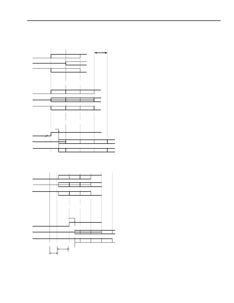
Lucent Technologies Inc.
43
Data Sheet
June 1999
ORCA Series 2 FPGAs
FPGA States of Operation
(continued)
5-2761(F).r4
Figure 38. Start-Up Waveforms
Partial Reconfiguration
All
ORCA
device families have been designed to allow
a partial reconfiguration of the FPGA at any time. This
is done by setting a bit stream option in the previous
configuration sequence that tells the FPGA to not reset
all of the configuration RAM during a reconfiguration.
Then only the configuration frames that are to be modi-
fied need to be rewritten, thereby reducing the configu-
ration time.
Other bit stream options are also available that allow
one portion of the FPGA to remain in operation while a
partial reconfiguration is being done. If this is done, the
user must be careful to not cause contention between
the two configurations (the bit stream resident in the
FPGA and the partial reconfiguration bit stream) as the
second reconfiguration bit stream is being loaded.
Other Configuration Options
Configuration options used during device start-up were
previously discussed in the FPGA States of Operation
section of this data sheet. There are many other config-
uration options available to the user that can be set
during bit stream generation in
ORCA
Foundry. These
include options to enable boundary scan, readback
options, and options to control and use the internal
oscillator after configuration.
Other useful options that affect the next configuration
(not the current configuration process) include options
to disable the global set/reset during configuration, dis-
able the 3-state of I/Os during configuration, and dis-
able the reset of internal RAMs during configuration to
allow for partial configurations (see above). For more
information on how to set these and other configuration
options, please see the
ORCA
Foundry documenta-
tion.
Configuration Data Format
The
ORCA
Foundry Development System interfaces
with front-end design entry tools and provides the tools
to produce a fully configured FPGA. This section dis-
cusses using the
ORCA
Foundry Development System
to generate configuration RAM data and then provides
the details of the configuration frame format.
The
ORCA
Series 2 series of FPGAs are enhanced
versions of the
ORCA
ATT2Cxx/ATT2Txx architectures
that provide upward bit stream compatibility for both
series of devices as well as with each other.
Di
F
DONE
ATT3000
I/O
GLOBAL
RESET
C1
C2
C3
C4
F
C1
C2
C3
C4
C1
C2
C3
C4
C1, C2, C3, OR C4
Di + 1
Di
Di + 2
Di + 3
Di + 4
Di + 1
Di
Di + 2
Di + 3
Di + 4
ORCA
CCLK_SYNC
DONE IN
U1
U2
U3
U4
F
U1
U2
U3
U4
U1
U2
U3
U4
ORCA
UCLK_NOSYNC
Di + 1
Di
Di + 2
Di + 3
Di + 4
Di + 1
Di + 2
Di + 3
ORCA
UCLK_SYNC
UCLK PERIOD
SYNCHRONIZATION UNCERTAINTY
DONE IN
F
C1
C1
U1, U2, U3, OR U4
DONE
I/O
GSRN
ACTIVE
DONE
I/O
GSRN
ACTIVE
DONE
I/O
GSRN
ACTIVE
DONE
I/O
GSRN
ACTIVE
UCLK
F = finished, no more CLKs required.
CCLK PERIOD
F
ORCA
CCLK_NOSYNC

Data Sheet
ORCA Series 2 FPGAs
June 1999
44
Lucent Technologies Inc.
Configuration Data Format
(continued)
Using
ORCA Foundry
to Generate
Configuration RAM Data
The configuration data defines the I/O functionality,
logic, and interconnections. The bit stream is gener-
ated by the development system. The bit stream cre-
ated by the bit stream generation tool is a series of 1s
and 0s used to write the FPGA configuration RAM. The
bit stream can be loaded into the FPGA using one of
the configuration modes discussed later. In the bit
stream generator, the designer selects options which
affect the FPGA's functionality. Using the output of the
bit stream generator, circuit.bit, the development sys-
tem's download tool can load the configuration data
into the
ORCA
series FPGA evaluation board from a
PC or workstation. Alternatively, a user can program a
PROM (such as the ATT1700A Series Serial ROM or a
standard EPROM) and load the FPGA from the PROM.
The development system's PROM programming tool
produces a file in .mks or .exo format.
Configuration Data Frame
A detailed description of the frame format is shown in
Figure 39. The header frame begins with a series of 1s
and a preamble of 0010, followed by a 24-bit length
count field representing the total number of configura-
tion clocks needed to complete the loading of the
FPGAs. Following the header frame is an optional ID
frame. This frame contains data used to determine if
the bit stream is being loaded to the correct type of
ORCA
FPGA (i.e., a bit stream generated for an
OR2C15A is being sent to an OR2C15A). Since the
OR2CxxA devices are bit stream compatible with the
ATT2Cxx, ATT2Txx, OR2TxxA, and OR2TxxB families,
a bit stream from any of these devices will not cause an
error when loaded into an OR2CxxA, OR2TxxA, or
OR2TxxB device. The ID frame has a secondary func-
tion of optionally enabling the parity checking logic for
the rest of the data frames.
The configuration data frames follow. Each frame starts
with a 0 start bit and ends with three or more 1 stop
bits. Following each start bit are four control bits: a pro-
gram bit, set to 1 if this is a data frame; a compress bit,
set to 1 if this is a compressed frame; and the opar and
epar parity bits (see Bit Stream Error Checking). An
11-bit address field that determines in which column
the FPGA is to be written is followed by alignment and
write control bits. For uncompressed frames, the data
bits needed to write one column in the FPGA are next.
For compressed frames, the data bits from the previous
frame are sent to a different FPGA column, as speci-
fied by the new address bits; therefore, new data bits
are not required. When configuration of the current
FPGA is finished, an end-of-configuration frame (where
the program bit is set to 0) is sent to the FPGA. The
length and number of data frames and information on
the PROM size for the Series 3 FPGAs are given in
Table 7.
Table 7. Configuration Frame Size
Devices
OR2C/
2T04A
OR2C/
2T06A
OR2C/
2T08A
OR2C/
2T10A
OR2C/
2T12A
OR2C/
2T15A/B
OR2C/
2T26A
OR2C/
2T40A/B
# of Frames
480
568
656
744
832
920
1096
1378
Data Bits/Frame
110
130
150
170
190
210
250
316
Configuration Data
(# of frames x # of data bits/frame)
52,800
73,840
98,400
126,480
158,080
193,200
274,000
435,448
Maximum Total # Bits/Frame
(align bits, 1 write bit, 8 stop bits)
136
160
176
200
216
240
280
344
Maximum Configuration Data
(# bits x # of frames)
65,280
90,880
115,456
148,800
179,712
220,800
306,880
474,032
Maximum PROM Size (bits)
(add 48-bit header, ID frame, and
40-bit end of configuration frame)
65,504
91,128
115,720
149,088
180,016
221,128
307,248
474,464

Data Sheet
June 1999
ORCA Series 2 FPGAs
Lucent Technologies Inc.
45
Configuration Data Format
(continued)
The data frames for all the Series 2 series devices are given in Table 8. An alignment field is required in the slave
parallel mode for the uncompressed format. The alignment field (shown by [A]) is a series of 0s: five for the
OR2C06A/OR2T06A, OR2C10A/OR2T10A, OR2C15A/OR2T15A/OR2T15B, and OR2C26A/OR2T26A; three for
the OR2C40A/OR2T40A/OR2T40B; and one for the OR2C04A/OR2T04A, OR2C08A/OR2T08A, and OR2C12A/
OR2T12A. The alignment field is not required in any other mode.
Table 8. Configuration Data Frames
5-4530(F)
Figure 39. Serial Configuration Data Format
OR2C04A/OR2T04A
Uncompressed
010 opar epar [addr10:0] [A]1[Data109:0]111
Compressed
011 opar epar [addr10:0] 111
OR2C06A/OR2T06A
Uncompressed
010 opar epar [addr10:0] [A]1[Data129:0]111
Compressed
011 opar epar [addr10:0] 111
OR2C08A/OR2T08A
Uncompressed
010 opar epar [addr10:0] [A]1[Data149:0]111
Compressed
011 opar epar [addr10:0] 111
OR2C10A/OR2T10A
Uncompressed
010 opar epar [addr10:0] [A]1[Data169:0]111
Compressed
011 opar epar [addr10:0] 111
OR2C12A/OR2T12A
Uncompressed
010 opar epar [addr10:0] [A]1[Data189:0]111
Compressed
011 opar epar [addr10:0] 111
OR2C15A/OR2T15A/OR2T15B
Uncompressed
010 opar epar [addr10:0] [A]1[Data209:0]111
Compressed
011 opar epar [addr10:0] 111
OR2C26A/OR2T26A
Uncompressed
010 opar epar [addr10:0] [A]1[Data249:0]111
Compressed
011 opar epar [addr10:0] 111
OR2C40A/OR2T40A/OR2T40B
Uncompressed
010 opar epar [addr10:0] [A]1[Data315:0]111
Compressed
011 opar epar [addr10:0] 111
EIGHT 1s
0010
24-bit
LENGTH
COUNT
POSTAMBLE
LEADING HEADER
DATA FRAMES
FPGA #1
DATA FRAMES
FPGA #2
END OF
CONFIGURATION
FRAME
FPGA #1
END OF
CONFIGURATION
FRAME
FPGA #2
PREAMBLE

Data Sheet
ORCA Series 2 FPGAs
June 1999
46
Lucent Technologies Inc.
Configuration Data Format
(continued)
Table 9. Configuration Frame Format and Contents
Note:
For slave parallel mode, the byte containing the preamble must be 11110010. The number of leading header dummy bits must
be (n
*
8) + 4, where n is any nonnegative integer and the number of trailing dummy bits must be (n
*
8), where n is any positive
integer. The number of stop bits/frame for slave parallel mode must be (x
*
8), where x is a positive integer. Note also that the bit
stream generator tool supplies a bit stream which is compatible with all configuration modes, including slave parallel mode.
Header
11111111
Leading header--4 bits minimum dummy bits
0010
Preamble
24-Bit Length Count
Configuration frame length
1111
Trailing header--4 bits minimum dummy bits
ID Frame
(Optional)
0
Frame start
P--1
Must be set to 1 to indicate data frame
C--0
Must be set to 0 to indicate uncompressed
Opar, Epar
Frame parity bits
Addr[10:0] =
11111111111
ID frame address
Prty_En
Set to 1 to enable parity
Reserved [42:0]
Reserved bits set to 0
ID
20-bit part ID
111
Three or more stop bits (high) to separate frames
Configuration
Data
Frame
(repeated for
each data frame)
0
Frame start
P--1 or 0
1 indicates data frame; 0 indicates all frames are written
C--1 or 0
Uncompressed--0 indicates data and address are supplied;
Compressed--1 indicates only address is supplied
Opar, Epar
Frame parity bits
Addr[10:0]
Column address in FPGA to be written
A
Alignment bit (different number of 0s needed for each part)
1
Write bit--used in uncompressed data frame
Data Bits
Needed only in an uncompressed data frame
.
.
.
.
111
One or more stop bits (high) to separate frames
End of
Configuration
0010011111111111
16 bits--00 indicates all frames are written
Postamble
111111 . . . . .
Additional 1s

Lucent Technologies Inc.
47
Data Sheet
June 1999
ORCA Series 2 FPGAs
Bit Stream Error Checking
There are three different types of bit stream error
checking performed in the
ORCA
Series 2 FPGAs:
ID frame, frame alignment, and parity checking.
An optional ID data frame can be sent to a specified
address in the FPGA. This ID frame contains a unique
code for the part it was generated for which is com-
pared within the FPGA. Any differences are flagged as
an ID error. This frame is automatically created by the
bit stream generation program in
ORCA
Foundry.
Every data frame in the FPGA begins with a start bit
set to 0 and three or more stop bits set to 1. If any of
the three previous bits were a 0 when a start bit is
encountered, it is flagged as a frame alignment error.
Parity checking is also done on the FPGA for each
frame, if it has been enabled by setting the prty_en bit
to 1 in the ID frame. This is set by enabling the parity
check option in the bit stream generation program of
ORCA
Foundry. Two parity bits, opar and epar, are
used to check the parity of bits in alternating bit posi-
tions to even parity in each data frame. If an odd num-
ber of ones is found for either the even bits (starting
with the start bit) or the odd bits (starting with the pro-
gram bit), then a parity error is flagged.
When any of the three possible errors occur, the FPGA
is forced into the INIT state, forcing
INIT
low. The FPGA
will remain in this state until either the
RESET
or
PRGM
pins are asserted.
FPGA Configuration Modes
There are eight methods for configuring the FPGA.
Seven of the configuration modes are selected on the
M0, M1, and M2 inputs. The eighth configuration mode
is accessed through the boundary-scan interface. A
fourth input, M3, is used to select the frequency of the
internal oscillator, which is the source for CCLK in
some configuration modes. The nominal frequencies of
the internal oscillator are 1.25 MHz and 10 MHz. The
1.25 MHz frequency is selected when the M3 input is
unconnected or driven to a high state.
There are three basic FPGA configuration modes:
master, slave, and peripheral. The configuration data
can be transmitted to the FPGA serially or in parallel
bytes. As a master, the FPGA provides the control sig-
nals out to strobe data in. As a slave device, a clock is
generated externally and provided into CCLK. In the
peripheral mode, the FPGA acts as a microprocessor
peripheral. Table 10 lists the functions of the configura-
tion mode pins.
Table 10. Configuration Modes
Master Parallel Mode
The master parallel configuration mode is generally
used to interface to industry-standard byte-wide mem-
ory, such as the 2764 and larger EPROMs. Figure 40
provides the connections for master parallel mode. The
FPGA outputs an 18-bit address on A[17:0] to memory
and reads one byte of configuration data on the rising
edge of RCLK. The parallel bytes are internally serial-
ized starting with the least significant bit, D0.
5-4483(F)
Figure 40. Master Parallel Configuration Schematic
There are two parallel master modes: master up and
master down. In master up, the starting memory
address is 00000 Hex and the FPGA increments the
address for each byte loaded. In master down, the
starting memory address is 3FFFF Hex and the FPGA
decrements the address.
One master mode FPGA can interface to the memory
and provide configuration data on DOUT to additional
FPGAs in a daisy chain. The configuration data on
DOUT is provided synchronously with the falling edge
of CCLK. The frequency of the CCLK output is eight
times that of RCLK.
M2
M1
M0
CCLK
Configuration
Mode
Data
0
0
0
Output
Master Serial
0
0
1
Input
Slave Parallel
Parallel
0
1
0
Reserved
0
1
1
Input
Sync Peripheral
Parallel
1
0
0
Output
Master (up)
Parallel
1
0
1
Output
Async Peripheral
Parallel
1
1
0
Output
Master (down)
Parallel
1
1
1
Input
Slave
Serial
TO DAISY-
CHAINED
DEVICES
DOUT
CCLK
HDC
LDC
RCLK
A[17:0]
D[7:0]
DONE
PRGM
M2
M1
M0
A[17:0]
D[7:0]
OE
CE
PROGRAM
V
DD
V
DD
OR GND
EPROM
ORCA
SERIES
FPGA
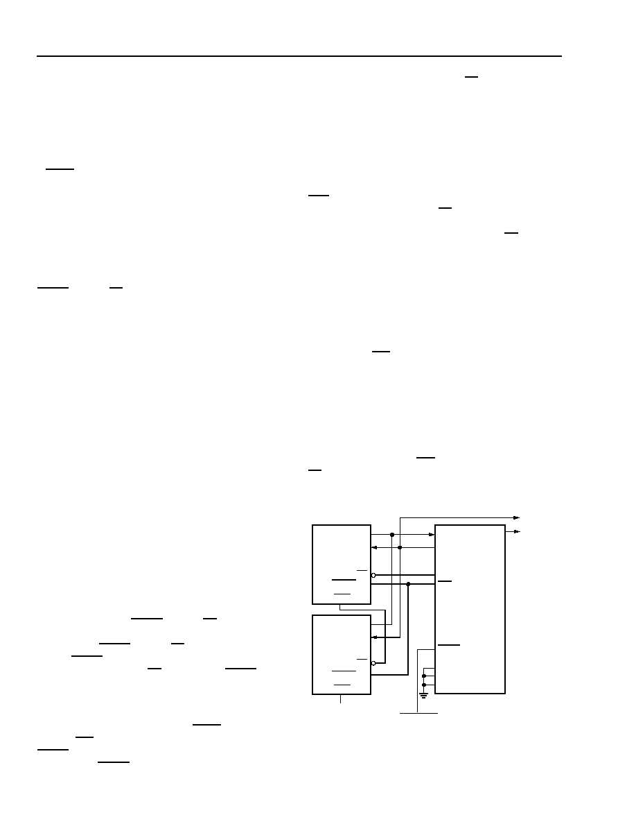
48
Lucent Technologies Inc.
Data Sheet
ORCA Series 2 FPGAs
June 1999
FPGA Configuration Modes
(continued)
Master Serial Mode
In the master serial mode, the FPGA loads the configu-
ration data from an external serial ROM. The configura-
tion data is either loaded automatically at start-up or on
a
PRGM
command to reconfigure. The ATT1700 and
ATT1700A Series can be used to configure the FPGA
in the master serial mode. This provides a simple 4-pin
interface in an 8-pin package. The ATT1736, ATT1765,
and ATT17128 serial ROMs store 32K, 64K, and 128K
bits, respectively.
Configuration in the master serial mode can be done at
powerup and/or upon a configure command. The sys-
tem or the FPGA must activate the serial ROM's
RESET
/OE and
CE
inputs. At powerup, the FPGA and
serial ROM each contain internal power-on reset cir-
cuitry that allows the FPGA to be configured without
the system providing an external signal. The power-on
reset circuitry causes the serial ROM's internal address
pointer to be reset. After powerup, the FPGA automati-
cally enters its initialization phase.
The serial ROM/FPGA interface used depends on such
factors as the availability of a system reset pulse, avail-
ability of an intelligent host to generate a configure
command, whether a single serial ROM is used or mul-
tiple serial ROMs are cascaded, whether the serial
ROM contains a single or multiple configuration pro-
grams, etc. Because of differing system requirements
and capabilities, a single FPGA/serial ROM interface is
generally not appropriate for all applications.
Data is read in the FPGA sequentially from the serial
ROM. The DATA output from the serial ROM is con-
nected directly into the DIN input of the FPGA. The
CCLK output from the FPGA is connected to the
CLOCK input of the serial ROM. During the configura-
tion process, CCLK clocks one data bit on each rising
edge.
Since the data and clock are direct connects, the
FPGA/serial ROM design task is to use the system or
FPGA to enable the
RESET
/OE and
CE
of the serial
ROM(s). There are several methods for enabling the
serial ROM's
RESET
/OE and
CE
inputs. The serial
ROM's
RESET
/OE is programmable to function with
RESET active-high and
OE
active-low or
RESET
active-
low and OE active-high.
In Figure 41, serial ROMs are cascaded to configure
multiple daisy-chained FPGAs. The host generates a
500 ns low pulse into the FPGA's
PRGM
input. The
FPGA's
INIT
input is connected to the serial ROM's
RESET
/OE input, which has been programmed to
function with
RESET
active-low and OE active-high.
The FPGA DONE is routed to the
CE
pin. The low on
DONE enables the serial ROMs. At the completion of
configuration, the high on the FPGA's DONE disables
the serial ROM.
Serial ROMs can also be cascaded to support the con-
figuration of multiple FPGAs or to load a single FPGA
when configuration data requirements exceed the
capacity of a single serial ROM. After the last bit from
the first serial ROM is read, the serial ROM outputs
CEO
low and 3-states the DATA output. The next serial
ROM recognizes the low on
CE
input and outputs con-
figuration data on the DATA output. After configuration
is complete, the FPGA's DONE output into
CE
disables
the serial ROMs.
This FPGA/serial ROM interface is not used in applica-
tions in which a serial ROM stores multiple configura-
tion programs. In these applications, the next
configuration program to be loaded is stored at the
ROM location that follows the last address for the previ-
ous configuration program. The reason the interface in
Figure 41 will not work in this application is that the low
output on the
INIT
signal would reset the serial ROM
address pointer, causing the first configuration to be
reloaded.
In some applications, there can be contention on the
FPGA's DIN pin. During configuration, DIN receives
configuration data, and after configuration, it is a user
I/O. If there is contention, an early DONE at start-up
(selected in
ORCA
Foundry) may correct the problem.
An alternative is to use
LDC
to drive the serial ROM's
CE
pin. In order to reduce noise, it is generally better to
run the master serial configuration at 1.25 MHz (M3 pin
tied high), rather than 10 MHz, if possible.
Figure 41. Master Serial Configuration Schematic
ATT1700A
DIN
M2
M1
M0
ORCA
SERIES
FPGA
CCLK
DOUT
TO DAISY-
CHAINED
DEVICES
DATA
CLK
CE
CEO
ATT1700A
DATA
CLK
RESET/OE
CEO
CE
TO MORE
SERIAL ROMs
AS NEEDED
DONE
INIT
PROGRAM
RESET/OE
PRGM
5-4456.1(F)
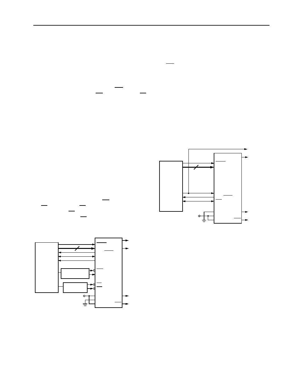
Lucent Technologies Inc.
49
Data Sheet
June 1999
ORCA Series 2 FPGAs
FPGA Configuration Modes
(continued)
Asynchronous Peripheral Mode
Figure 42 shows the connections needed for the asyn-
chronous peripheral mode. In this mode, the FPGA
system interface is similar to that of a microprocessor-
peripheral interface. The microprocessor generates the
control signals to write an 8-bit byte into the FPGA. The
FPGA control inputs include active-low
CS0
and active-
high CS1 chip selects, a write
WR
input, and a read
RD
input. The chip selects can be cycled or maintained at
a static level during the configuration cycle. Each byte
of data is written into the FPGA's D[7:0] input pins.
The FPGA provides a RDY status output to indicate
that another byte can be loaded. A low on RDY indi-
cates that the double-buffered hold/shift registers are
not ready to receive data, and this pin must be moni-
tored to go high before another byte of data can be
written. The shortest time RDY is low occurs when a
byte is loaded into the hold register and the shift regis-
ter is empty, in which case the byte is immediately
transferred to the shift register. The longest time for
RDY to remain low occurs when a byte is loaded into
the holding register and the shift register has just
started shifting configuration data into configuration
RAM.
The RDY status is also available on the D7 pin by
enabling the chip selects, setting
WR
high, and apply-
ing
RD
low, where the
RD
input is an output enable for
the D7 pin when
RD
is low. The D[6:0] pins are not
enabled to drive when
RD
is low and, thus, only act as
input pins in asynchronous peripheral mode.
5-4484(F)
Figure 42. Asynchronous Peripheral Configuration
Schematic
Synchronous Peripheral Mode
In the synchronous peripheral mode, byte-wide data is
input into D[7:0] on the rising edge of the CCLK input.
The first data byte is clocked in on the second CCLK
after
INIT
goes high. Subsequent data bytes are
clocked in on every eighth rising edge of CCLK. The
RDY signal is an output which acts as an acknowledge.
RDY goes high one CCLK after data is clocked and,
after one CCLK cycle, returns low. The process repeats
until all of the data is loaded into the FPGA. The data
begins shifting on DOUT 1.5 cycles after it is loaded in
parallel. It requires additional CCLKs after the last byte
is loaded to complete the shifting. Figure 43 shows the
connections for synchronous peripheral mode.
As with master modes, the peripheral modes can be
used as the lead FPGA for a daisy chain of slave
FPGAs.
5-4486(F)
Figure 43. Synchronous Peripheral Configuration
Schematic
TO DAISY-
CHAINED
DEVICES
DOUT
CCLK
HDC
LDC
V
DD
ORCA
SERIES
FPGA
MICRO-
PROCESSOR
ADDRESS
DECODE LOGIC
BUS
CONTROLLER
PRGM
D[7:0]
RDY/BUSY
INIT
DONE
CS0
CS1
RD
WR
M2
M1
M0
8
TO DAISY-
CHAINED
DEVICES
DOUT
HDC
LDC
ORCA
SERIES
FPGA
MICRO-
PROCESSOR
PRGM
D[7:0]
M2
M1
M0
8
+5 V
CCLK
RDY/BUSY
INIT

50
Lucent Technologies Inc.
Data Sheet
ORCA Series 2 FPGAs
June 1999
FPGA Configuration Modes
(continued)
Slave Serial Mode
The slave serial mode is primarily used when multiple
FPGAs are configured in a daisy chain. The serial
slave serial mode is also used on the FPGA evaluation
board which interfaces to the download cable. A device
in the slave serial mode can be used as the lead device
in a daisy chain. Figure 44 shows the connections for
the slave serial configuration mode.
The configuration data is provided into the FPGA's DIN
input synchronous with the configuration clock CCLK
input. After the FPGA has loaded its configuration data,
it retransmits the incoming configuration data on
DOUT. CCLK is routed into all slave serial mode
devices in parallel.
Multiple slave FPGAs can be loaded with identical con-
figurations simultaneously. This is done by loading the
configuration data into the DIN inputs in parallel.
5-4485(F)
Figure 44. Slave Serial Configuration Schematic
Slave Parallel Mode
The slave parallel mode is essentially the same as the
slave serial mode except that 8 bits of data are input on
pins D[7:0] for each CCLK cycle. Due to 8 bits of data
being input per CCLK cycle, the DOUT pin does not
contain a valid bit stream for slave parallel mode. As a
result, the lead device cannot be used in the slave
parallel mode in a daisy-chain configuration.
Figure 45 is a schematic of the connections for the
slave parallel configuration mode.
WR
and
CS0
are
active-low chip select signals, and CS1 is an active-
high chip select signal. These chip selects allow the
user to configure multiple FPGAs in slave parallel
mode using an 8-bit data bus common to all of the
FPGAs. These chip selects can then be used to select
the FPGA(s) to be configured with a given bit stream,
but once an FPGA has been selected, it cannot be
deselected until it has been completely programmed.
5-4487(F)
Figure 45. Slave Parallel Configuration Schematic
MICRO-
PROCESSOR
OR
DOWNLOAD
CABLE
M2
M1
M0
HDC
SERIES
FPGA
LDC
V
DD
CCLK
PRGM
DOUT
TO DAISY-
CHAINED
DEVICES
DONE
DIN
INIT
ORCA
MICRO-
PROCESSOR
OR
SYSTEM
D[7:0]
DONE
CCLK
CS1
M2
M1
M0
HDC
LDC
8
V
DD
INIT
PRGM
CS0
WR
SERIES
FPGA
ORCA

Data Sheet
June 1999
ORCA Series 2 FPGAs
Lucent Technologies Inc.
51
FPGA Configuration Modes
(continued)
Daisy Chain
Multiple FPGAs can be configured by using a daisy
chain of the FPGAs. Daisy chaining uses a lead FPGA
and one or more FPGAs configured in slave serial
mode. The lead FPGA can be configured in any mode
except slave parallel mode. (Daisy chaining is not avail-
able with the boundary-scan ram_w instruction, dis-
cussed later.)
All daisy-chained FPGAs are connected in series.
Each FPGA reads and shifts the preamble and length
count in on positive CCLK and out on negative CCLK
edges.
An upstream FPGA that has received the preamble
and length count outputs a high on DOUT until it has
received the appropriate number of data frames so that
downstream FPGAs do not receive frame start bits
(0s). After loading and retransmitting the preamble and
length count to a daisy chain of slave devices, the lead
device loads its configuration data frames. The loading
of configuration data continues after the lead device
has received its configuration data if its internal frame
bit counter has not reached the length count. When the
configuration RAM is full and the number of bits
received is less than the length count field, the FPGA
shifts any additional data out on DOUT.
The configuration data is read into DIN of slave devices
on the positive edge of CCLK, and shifted out DOUT
on the negative edge of CCLK. Figure 46 shows the
connections for loading multiple FPGAs in a daisy-
chain configuration.
The generation of CCLK for the daisy-chained devices
which are in slave serial mode differs depending on the
configuration mode of the lead device. A master paral-
lel mode device uses its internal timing generator to
produce an internal CCLK at eight times its memory
address rate (RCLK). The asynchronous peripheral
mode device outputs eight CCLKs for each write cycle.
If the lead device is configured in either synchronous
peripheral or a slave mode, CCLK is routed to the lead
device and to all of the daisy-chained devices.
The development system can create a composite
configuration bit stream for configuring daisy-chained
FPGAs. The frame format is a preamble, a length count
for the total bit stream, multiple concatenated data
frames, an end-of-configuration frame per device, a
postamble, and an additional fill bit per device in the
serial chain.
As seen in Figure 46, the
INIT
pins for all of the FPGAs
are connected together. This is required to guarantee
that powerup and initialization will work correctly. In
general, the DONE pins for all of the FPGAs are also
connected together as shown to guarantee that all of
the FPGAs enter the start-up state simultaneously. This
may not be required, depending upon the start-up
sequence desired.
5-4488(F)
Figure 46. Daisy-Chain Configuration Schematic
V
DD
EPROM
PROGRAM
D[7:0]
OE
CE
A[17:0]
A[17:0]
D[7:0]
DONE
M2
M1
M0
DONE
HDC
LDC
RCLK
CCLK
DOUT
DIN
DOUT
DIN
CCLK
DONE
DOUT
INIT
INIT
INIT
CCLK
V
DD
V
DD
OR
GND
PRGM
PRGM
M2
M1
M0
PRGM
M2
M1
M0
V
DD
V
DD
HDC
LDC
RCLK
HDC
LDC
RCLK
V
DD
ORCA
SERIES
FPGA
SLAVE #2
ORCA
SERIES
FPGA
MASTER
ORCA
SERIES
FPGA
SLAVE #1

52
Lucent Technologies Inc.
Data Sheet
ORCA Series 2 FPGAs
June 1999
Special Function Blocks
Special function blocks in the Series 2 provide extra
capabilities beyond general FPGA operation. These
blocks reside in the corners of the FPGA array.
Single Function Blocks
Most of the special function blocks perform a specific
dedicated function. These functions are data/configura-
tion readback control, global 3-state control (TS_ALL),
internal oscillator generation, global set/reset (GSRN),
and start-up logic.
Readback Logic
The readback logic is located in the upper right corner
of the FPGA.
Readback is used to read back the configuration data
and, optionally, the state of the PFU outputs. A read-
back operation can be done while the FPGA is in nor-
mal system operation. The readback operation cannot
be daisy-chained. To use readback, the user selects
options in the bit stream generator in the
ORCA
Foundry Development System.
Table 11 provides readback options selected in the bit
stream generator tool. The table provides the number
of times that the configuration data can be read back.
This is intended primarily to give the user control over
the security of the FPGA's configuration program. The
user can prohibit readback (0), allow a single readback
(1), or allow unrestricted readback (U).
Table 11. Readback Options
The pins used for readback are readback data
(RD_DATA), read configuration (
RD_CFG
), and configu-
ration clock (CCLK). A readback operation is initiated
by a high-to-low transition on
RD_CFG
. The
RD_CFG
input must remain low during the readback operation.
The readback operation can be restarted at frame 0 by
driving the
RD_CFG
pin high, applying at least two ris-
ing edges of CCLK, and then driving
RD_CFG
low
again. One bit of data is shifted out on RD_DATA at the
rising edge of CCLK. The first start bit of the readback
frame is transmitted out several cycles after the first ris-
ing edge of CCLK after
RD_CFG
is input low (see Table
48, Readback Timing Characteristics in the Timing
Characteristics section).
It should be noted that the RD_DATA output pin is also
used as the dedicated boundary-scan output pin, TDO.
If this pin is being used as TDO, the RD_DATA output
from readback can be routed internally to any other pin
desired. The
RD_CFG
input pin is also used to control
the global 3-state (TS_ALL) function. Before and during
configuration, the TS_ALL signal is always driven by
the
RD_CFG
input and readback is disabled. After con-
figuration, the selection as to whether this input drives
the readback or global 3-state function is determined
by a set of bit stream options. If used as the
RD_CFG
input for readback, the internal TS_ALL input can be
routed internally to be driven by any input pin.
The readback frame contains the configuration data
and the state of the internal logic. During readback, the
value of all five PFU outputs can be captured. The fol-
lowing options are allowed when doing a capture of the
PFU outputs.
1. Do not capture data (the data written to the capture
RAMs, usually 0, will be read back).
2. Capture data upon entering readback.
3. Capture data based upon a configurable signal
internal to the FPGA. If this signal is tied to
logic 0, capture RAMs are written continuously.
4. Capture data on either options 2 or 3 above.
The readback frame has a similar, but not identical, for-
mat to the configuration frame. This eases a bitwise
comparison between the configuration and readback
data. The readback data is not inverted. Every data
frame has one low start bit and one high stop bit. The
preamble, including the length count field, is not part of
the readback frame. The readback frame contains
states in locations not used in the configuration. These
locations need to be masked out when comparing the
configuration and readback frames. The development
system optionally provides a readback bit stream to
compare to readback from the FPGA. Also note that if
any of the LUTs are used as RAM and new data is writ-
ten to them, these bits will not have the same values as
the original configuration data frame either.
Option
Function
0
Prohibit Readback
1
Allow One Readback Only
U
Allow Unrestricted Number of Readbacks

Lucent Technologies Inc.
53
Data Sheet
June 1999
ORCA Series 2 FPGAs
Special Function Blocks
(continued)
Global 3-State Control (TS_ALL)
The TS_ALL block resides in the upper-right corner of
the FPGA array.
To increase the testability of the
ORCA
Series FPGAs,
the global 3-state function (TS_ALL) disables the
device. The TS_ALL signal is driven from either an
external pin or an internal signal. Before and during
configuration, the TS_ALL signal is driven by the input
pad
RD_CFG
. After configuration, the TS_ALL signal
can be disabled, driven from the
RD_CFG
input pad, or
driven by a general routing signal in the upper-right cor-
ner. Before configuration, TS_ALL is active-low; after
configuration, the sense of TS_ALL can be inverted.
The following occur when TS_ALL is activated:
1. All of the user I/O output buffers are 3-stated, the
user I/O input buffers are pulled up (with the pull-
down disabled), and the input buffers are configured
with TTL input thresholds (OR2CxxA only).
2. The TDO/RD_DATA output buffer is 3-stated.
3. The
RD_CFG
,
RESET
, and
PRGM
input buffers remain
active with a pull-up.
4. The DONE output buffer is 3-stated, and the input
buffer is pulled-up.
Internal Oscillator
The internal oscillator resides in the lower-left corner of
the FPGA array. It has output clock frequencies of
1.25 MHz and 10 MHz. The internal oscillator is the
source of the internal CCLK used for configuration. It
may also be used after configuration as a general-
purpose clock signal.
Global Set/Reset (GSRN)
The GSRN logic resides in the lower-right corner of the
FPGA. GSRN is an invertible, default, active-low signal
that is used to reset all of the user-accessible latches/
FFs on the device. GSRN is automatically asserted at
powerup and during configuration of the device.
The timing of the release of GSRN at the end of config-
uration can be programmed in the start-up logic
described below. Following configuration, GSRN may
be connected to the
RESET
pin via dedicated routing,
or it may be connected to any signal via normal routing.
Within each PFU, individual FFs and latches can be
programmed to either be set or reset when GSRN is
asserted.
The
RESET
input pad has a special relationship to
GSRN. During configuration, the
RESET
input pad
always initiates a configuration abort, as described in
the FPGA States of Operation section. After configura-
tion, the global set/reset signal (GSRN) can either be
disabled (the default), directly connected to the
RESET
input pad, or sourced by a lower-right corner signal. If
the
RESET
input pad is not used as a global reset after
configuration, this pad can be used as a normal input
pad.
Start-Up Logic
The start-up logic block is located in the lower right cor-
ner of the FPGA. This block can be configured to coor-
dinate the relative timing of the release of GSRN, the
activation of all user I/Os, and the assertion of the
DONE signal at the end of configuration. If a start-up
clock is used to time these events, the start-up clock
can come from CCLK, or it can be routed into the start-
up block using lower-right corner routing resources.
These signals are described in the Start-Up subsection
of the FPGA States of Operation section.

54
Lucent Technologies Inc.
Data Sheet
ORCA Series 2 FPGAs
June 1999
Special Function Blocks
(continued)
Boundary Scan
The increasing complexity of integrated circuits (ICs)
and IC packages has increased the difficulty of testing
printed-circuit boards (PCBs). To address this testing
problem, the
IEEE
standard 1149.1 - 1990 (
IEEE
Stan-
dard Test Access Port and Boundary-Scan Architec-
ture) is implemented in the
ORCA
series of FPGAs. It
allows users to efficiently test the interconnection
between integrated circuits on a PCB as well as test
the integrated circuit itself. The
IEEE
1149.1 standard
is a well-defined protocol that ensures interoperability
among boundary-scan (BSCAN) equipped devices
from different vendors.
The
IEEE
1149.1 standard defines a test access port
(TAP) that consists of a 4-pin interface with an optional
reset pin for boundary-scan testing of integrated cir-
cuits in a system. The
ORCA
series FPGA provides
four interface pins: test data in (TDI), test mode select
(TMS), test clock (TCK), and test data out (TDO). The
PRGM
pin used to reconfigure the device also resets
the boundary-scan logic.
The user test host serially loads test commands and
test data into the FPGA through these pins to drive out-
puts and examine inputs. In the configuration shown in
Figure 47, where boundary scan is used to test ICs,
test data is transmitted serially into TDI of the first
BSCAN device (U1), through TDO/TDI connections
between BSCAN devices (U2 and U3), and out TDO of
the last BSCAN device (U4). In this configuration, the
TMS and TCK signals are routed to all boundary-scan
ICs in parallel so that all boundary-scan components
operate in the same state. In other configurations, mul-
tiple scan paths are used instead of a single ring. When
multiple scan paths are used, each ring is indepen-
dently controlled by its own TMS and TCK signals.
Figure 48 provides a system interface for components
used in the boundary-scan testing of PCBs. The three
major components shown are the test host, boundary-
scan support circuit, and the devices under test
(DUTs). The DUTs shown here are
ORCA
Series
FPGAs with dedicated boundary-scan circuitry. The
test host is normally one of the following: automatic test
equipment (ATE), a workstation, a PC, or a micropro-
cessor.
Fig.34.a(F).1C
Key:
BSC = boundary-scan cell, BDC = bidirectional data cell,
and DCC = data control cell.
Figure 47. Printed-Circuit Board with Boundary-
Scan Circuitry
The boundary-scan support circuit shown in Figure 48
is the 497AA Boundary-Scan Master (BSM). The BSM
off-loads tasks from the test host to increase test
throughput. To interface between the test host and the
DUTs, the BSM has a general microprocessor interface
and provides parallel-to-serial/serial-to-parallel conver-
sion, as well as three 8K data buffers.
SCAN
OUT
TDI
TMS
TCK
TDO
U2
SEE ENLARGED VIEW BELOW
PLC
ARRAY
SCAN
IN
TDO TCK TMS TDI
TAPC
BYPASS
REGISTER
INSTRUCTION
REGISTER
BDC
BSC
P_IN
P_OUT
P_TS
SCAN
IN
PT[ij]
ENLARGED VIEW
TDI
TDO
TMS
TCK
U1
TDI
TDO
TMS
TCK
U4
TDI
TDO
TMS
TCK
U3
TDI
TDO
TMS
TCK
net a
net b
net c
s
DCC
SCAN
OUT
DCC
BSC
P_IN
P_OUT
P_TS
SCAN
IN
PB[ij]
BDC
SCAN
OUT
BDC
BSC
P_IN
P_OUT
P_TS
PR[ij]
DCC
SCAN
OUT
BSC
P_IN
P_OUT
P_TS
PL[ij]
SCAN
IN
DCC
BDC

Data Sheet
June 1999
ORCA Series 2 FPGAs
Lucent Technologies Inc.
55
Special Function Blocks
(continued)
5-4488(F)
Figure 48. Boundary-Scan Interface
V
DD
EPROM
PROGRAM
D[7:0]
OE
CE
A[17:0]
A[17:0]
D[7:0]
DONE
M2
M1
M0
DONE
HDC
LDC
RCLK
CCLK
DOUT
DIN
DOUT
DIN
CCLK
DONE
DOUT
INIT
INIT
INIT
CCLK
V
DD
V
DD
OR
GND
PRGM
PRGM
M2
M1
M0
PRGM
M2
M1
M0
V
DD
V
DD
HDC
LDC
RCLK
HDC
LDC
RCLK
V
DD
ORCA
SERIES
FPGA
SLAVE #2
ORCA
SERIES
FPGA
MASTER
ORCA
SERIES
FPGA
SLAVE #1
The BSM also increases test throughput with a dedi-
cated automatic test-pattern generator and with com-
pression of the test response with a signature analysis
register. The PC-based boundary-scan test card/soft-
ware allows a user to quickly prototype a boundary-
scan test setup.
Boundary-Scan Instructions
The
ORCA
Series boundary-scan circuitry is used for
three mandatory
IEEE
1149.1 tests (EXTEST, SAM-
PLE/PRELOAD, BYPASS) and four
ORCA
-defined
instructions. The 3-bit wide instruction register sup-
ports the eight instructions listed in Table 12.
Table 12. Boundary-Scan Instructions
The external test (EXTEST) instruction allows the inter-
connections between ICs in a system to be tested for
opens and stuck-at faults. If an EXTEST instruction is
performed for the system shown in Figure 47, the con-
nections between U1 and U2 (shown by nets a, b, and
c) can be tested by driving a value onto the given nets
from one device and then determining whether the
same value is seen at the other device. This is deter-
mined by shifting 2 bits of data for each pin (one for the
output value and one for the 3-state value) through the
BSR until each one aligns to the appropriate pin.
Then, based upon the value of the 3-state signal, either
the I/O pad is driven to the value given in the BSR, or
the BSR is updated with the input value from the I/O
pad, which allows it to be shifted out TDO.
The SAMPLE instruction is useful for system debug-
ging and fault diagnosis by allowing the data at the
FPGA's I/Os to be observed during normal operation.
The data for all of the I/Os is captured simultaneously
into the BSR, allowing them to be shifted-out TDO to
the test host. Since each I/O buffer in the PICs is bidi-
rectional, two pieces of data are captured for each I/O
pad: the value at the I/O pad and the value of the
3-state control signal.
Code
Instruction
000
EXTEST
001
PLC Scan Ring 1
010
RAM Write (RAM_W)
011
Reserved
100
SAMPLE/PRELOAD
101
PLC Scan Ring 2
110
RAM Read (RAM_R)
111
BYPASS
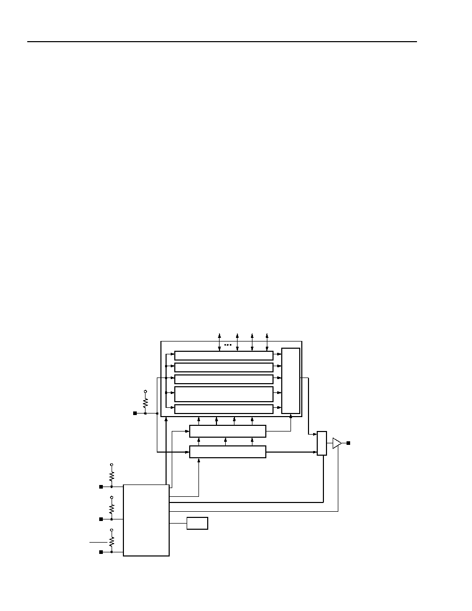
Data Sheet
ORCA Series 2 FPGAs
June 1999
56
Lucent Technologies Inc.
Special Function Blocks
(continued)
There are four
ORCA
-defined instructions. The PLC
scan rings 1 and 2 (PSR1, PSR2) allow user-defined
internal scan paths using the PLC latches/FFs. The
RAM_Write Enable (RAM_W) instruction allows the
user to serially configure the FPGA through TDI. The
RAM_Read Enable (RAM_R) allows the user to read
back RAM contents on TDO after configuration.
ORCA Boundary-Scan Circuitry
The
ORCA
Series boundary-scan circuitry includes a
test access port controller (TAPC), instruction register
(IR), boundary-scan register (BSR), and bypass regis-
ter. It also includes circuitry to support the four pre-
defined instructions.
Figure 49 shows a functional diagram of the boundary-
scan circuitry that is implemented in the
ORCA
series.
The input pins' (TMS, TCK, and TDI) locations vary
depending on the part, and the output pin is the dedi-
cated TDO/RD_DATA output pad. Test data in (TDI) is
the serial input data. Test mode select (TMS) controls
the boundary-scan test access port controller (TAPC).
Test clock (TCK) is the test clock on the board.
The BSR is a series connection of boundary-scan cells
(BSCs) around the periphery of the IC. Each I/O pad on
the FPGA, except for CCLK, DONE, and the boundary-
scan pins (TCK, TDI, TMS, and TDO), is included in
the BSR. The first BSC in the BSR (connected to TDI)
is located in the first PIC I/O pad on the left of the top
side of the FPGA (PTA PIC). The BSR proceeds clock-
wise around the top, right, bottom, and left sides of the
array. The last BSC in the BSR (connected to TDO) is
located on the top of the left side of the array (PLA3).
The bypass instruction uses a single FF which resyn-
chronizes test data that is not part of the current scan
operation. In a bypass instruction, test data received on
TDI is shifted out of the bypass register to TDO. Since
the BSR (which requires a two FF delay for each pad)
is bypassed, test throughput is increased when devices
that are not part of a test operation are bypassed.
The boundary-scan logic is enabled before and during
configuration. After configuration, a configuration
option determines whether or not boundary-scan logic
is used.
The 32-bit boundary-scan identification register con-
tains the manufacturer's ID number, unique part num-
ber, and version, but is not implemented in the
ORCA
series of FPGAs. If boundary scan is not used, TMS,
TDI, and TCK become user I/Os, and TDO is 3-stated
or used in the readback operation.
5-2840(C).r7
Figure 49.
ORCA
Series Boundary-Scan Circuitry Functional Diagram
TAP
CONTROLLER
BOUNDARY-SCAN REGISTER
PSR2 REGISTER (PLCs)
BYPASS REGISTER
DATA
MUX
INSTRUCTION DECODER
INSTRUCTION REGISTER
M
U
X
RESET
CLOCK-IR
SHIFT-IR
UPDATE-IR
PUR
TDO
SELECT
ENABLE
RESET
CLOCK-DR
SHIFT-DR
UPDATE-DR
TDI
DATA REGISTERS
PSR1 REGISTER (PLCs)
CONFIGURATION REGISTER
(RAM_R, RAM_W)
I/O BUFFERS
V
DD
TMS
V
DD
TCK
V
DD
PRGM
V
DD

Lucent Technologies Inc.
57
Data Sheet
June 1999
ORCA Series 2 FPGAs
Special Function Blocks
(continued)
ORCA
Series TAP Controller (TAPC)
The
ORCA
Series TAP controller (TAPC) is a 1149.1
compatible test access port controller. The 16 JTAG
state assignments from the
IEEE
1149.1 specification
are used. The TAPC is controlled by TCK and TMS.
The TAPC states are used for loading the IR to allow
three basic functions in testing: providing test stimuli
(Update-DR), test execution (Run-Test/Idle), and
obtaining test responses (Capture-DR). The TAPC
allows the test host to shift in and out both instructions
and test data/results. The inputs and outputs of the
TAPC are provided in the table below. The outputs are
primarily the control signals to the instruction register
and the data register.
Table 13. TAP Controller Input/Outputs
The TAPC generates control signals which allow cap-
ture, shift, and update operations on the instruction and
data registers. In the capture operation, data is loaded
into the register. In the shift operation, the captured
data is shifted out while new data is shifted in. In the
update operation, either the instruction register is
loaded for instruction decode, or the boundary-scan
register is updated for control of outputs.
The test host generates a test by providing input into
the
ORCA
Series TMS input synchronous with TCK.
This sequences the TAPC through states in order to
perform the desired function on the instruction register
or a data register. Figure 50 provides a diagram of the
state transitions for the TAPC. The next state is deter-
mined by the TMS input value.
5-5370(F)
Figure 50. TAP Controller State Transition Diagram
Symbol
I/O
Function
TMS
I
Test Mode Select
TCK
I
Test Clock
PUR
I
Powerup Reset
PRGM
I
BSCAN Reset
TRESET
O
Test Logic Reset
Select
O
Select IR (high); Select DR (low)
Enable
O
Test Data Out Enable
Capture-DR
O
Capture/Parallel Load DR
Capture-IR
O
Capture/Parallel Load IR
Shift-DR
O
Shift Data Register
Shift-DR
O
Shift Instruction Register
Update-DR
O
Update/Parallel Load DR
Update-IR
O
Update/Parallel Load IR
SELECT-
DR-SCAN
CAPTURE-DR
SHIFT-DR
EXIT1-DR
PAUSE-DR
EXIT2-DR
UPDATE-DR
1
1
0
0
1
0
RUN-TEST/
IDLE
1
TEST-LOGIC-
RESET
SELECT-
IR-SCAN
CAPTURE-IR
SHIFT-IR
EXIT1-IR
PAUSE-IR
EXIT2-IR
UPDATE-IR
1
1
0
1
0
0
0
0
0
1
0
1
1
1
0
1
1
0
0
0
0
1
1
1
0

Data Sheet
ORCA Series 2 FPGAs
June 1999
58
Lucent Technologies Inc.
Special Function Blocks
(continued)
Boundary-Scan Cells
Figure 51 is a diagram of the boundary-scan cell (BSC)
in the
ORCA
series PICs. There are four BSCs in each
PIC: one for each pad, except as noted above. The
BSCs are connected serially to form the BSR. The
BSC controls the functionality of the in, out, and 3-state
signals for each pad.
The BSC allows the I/O to function in either the normal
or test mode. Normal mode is defined as when an out-
put buffer receives input from the PLC array and pro-
vides output at the pad or when an input buffer
provides input from the pad to the PLC array. In the test
mode, the BSC executes a boundary-scan operation,
such as shifting in scan data from an upstream BSC in
the BSR, providing test stimuli to the pad, capturing
test data at the pad, etc.
The primary functions of the BSC are shifting scan data
serially in the BSR and observing input (P_IN), output
(P_OUT), and 3-state (P_TS) signals at the pads. The
BSC consists of two circuits: the bidirectional data cell
is used to access the input and output data, and the
direction control cell is used to access the 3-state
value. Both cells consist of a flip-flop used to shift scan
data which feeds a flip-flop to control the I/O buffer. The
bidirectional data cell is connected serially to the direc-
tion control cell to form a boundary-scan shift register.
The TAPC signals (capture, update, shiftn, treset, and
TCK) and the MODE signal control the operation of the
BSC. The bidirectional data cell is also controlled by
the high out/low in (HOLI) signal generated by the
direction control cell. When HOLI is low, the bidirec-
tional data cell receives input buffer data into the BSC.
When HOLI is high, the BSC is loaded with functional
data from the PLC.
The MODE signal is generated from the decode of the
instruction register. When the MODE signal is high
(EXTEST), the scan data is propagated to the output
buffer. When the MODE signal is low (BYPASS or
SAMPLE), functional data from the FPGA's internal
logic is propagated to the output buffer.
The boundary-scan description language (BSDL) is
provided for each device in the
ORCA
series of FPGAs.
The BSDL is generated from a device profile, pinout,
and other boundary-scan information.
5-2844(F).r4
Figure 51. Boundary-Scan Cell
D
Q
D
Q
D
Q
D
Q
SCAN IN
P_OUT
HOLI
BIDIRECTIONAL DATA CELL
I/O BUFFER
DIRECTION CONTROL CELL
MODE
UPDATE/TCK
SCAN OUT
TCK
SHIFTN/CAPTURE
P_TS
P_IN
PAD_IN
PAD_TS
PAD_OUT
0
1
0
1
0
1
0
1
0
1

Data Sheet
June 1999
ORCA Series 2 FPGAs
Lucent Technologies Inc.
59
Special Function Blocks
(continued)
Fig.5.3(F)
Figure 52. Instruction Register Scan Timing Diagram
Boundary-Scan Timing
To ensure race-free operation, data changes on specific clock edges. The TMS and TDI inputs are clocked in on
the rising edge of TCK, while changes on TDO occur on the falling edge of TCK. In the execution of an EXTEST
instruction, parallel data is output from the BSR to the FPGA pads on the falling edge of TCK. The maximum fre-
quency allowed for TCK is 10 MHz.
Figure 52 shows timing waveforms for an instruction scan operation. The diagram shows the use of TMS to
sequence the TAPC through states. The test host (or BSM) changes data on the falling edge of TCK, and it is
clocked into the DUT on the rising edge.
TE
ST
-LO
G
I
C
-
RES
E
T
RUN-TES
T
/IDLE
SE
LECT-DR-S
C
AN
CAP
T
UR
E-IR
S
H
IFT
-I
R
EX
IT
1-I
R
PA
USE
-
IR
EX
IT
2-I
R
S
H
IFT
-I
R
EX
IT
1-I
R
UPDA
T
E
-IR
RUN-TE
ST/
I
DLE
SE
LECT
-I
R-SCA
N
TCK
TMS
TDI

60
Lucent Technologies Inc.
Data Sheet
ORCA Series 2 FPGAs
June 1999
ORCA Timing Characteristics
To define speed grades, the
ORCA
Series part number
designation (see Table 54) uses a single-digit number
to designate a speed grade. This number is not related
to any single ac parameter. Higher numbers indicate a
faster set of timing parameters. The actual speed sort-
ing is based on testing the delay in a path consisting of
an input buffer, combinatorial delay through all PLCs in
a row, and an output buffer. Other tests are then done
to verify other delay parameters, such as routing
delays, setup times to FFs, etc.
The most accurate timing characteristics are reported
by the timing analyzer in the
ORCA
Foundry Develop-
ment System. A timing report provided by the develop-
ment system after layout divides path delays into logic
and routing delays. The timing analyzer can also pro-
vide logic delays prior to layout. While this allows rout-
ing budget estimates, there is wide variance in routing
delays associated with different layouts.
The logic timing parameters noted in the Electrical
Characteristics section of this data sheet are the same
as those in the design tools. In the PFU timing given in
Tables 31--79, symbol names are generally a concate-
nation of the PFU operating mode (as defined in
Table 3) and the parameter type. The wildcard charac-
ter (*) is used in symbol names to indicate that the
parameter applies to any sub-LUT. The setup, hold,
and propagation delay parameters, defined below, are
designated in the symbol name by the SET, HLD, and
DEL characters, respectively.
The values given for the parameters are the same as
those used during production testing and speed bin-
ning of the devices. The junction temperature and sup-
ply voltage used to characterize the devices are listed
in the delay tables. Actual delays at nominal tempera-
ture and voltage for best-case processes can be much
better than the values given.
It should be noted that the junction temperature used in
the tables is generally 85 ∞C. The junction temperature
for the FPGA depends on the power dissipated by the
device, the package thermal characteristics (
JA
), and
the ambient temperature, as calculated in the following
equation and as discussed further in the Package
Thermal Characteristics section:
T
Jmax =
T
Amax
+ (P ∑
JA
) ∞C
Note: The user must determine this junction tempera-
ture to see if the delays from
ORCA
Foundry
should be derated based on the following derat-
ing tables.
Table 14A and 14B and provide approximate power
supply and junction temperature derating for OR2CxxA
commercial and industrial devices. Table 15A and 15B
provides the same information for the OR2TxxA and
OR2TxxB devices (both commercial and industrial).
The delay values in this data sheet and reported by
ORCA
Foundry are shown as 1.00 in the tables. The
method for determining the maximum junction temper-
ature is defined in the Thermal Characteristics section.
Taken cumulatively, the range of parameter values for
best-case vs. worst-case processing, supply voltage,
and junction temperature can approach 3 to 1.
Table 14A. Derating for Commercial Devices
(OR2CxxA)
Table 14B. Derating for Industrial Devices
(OR2CxxA)
Table 15A. Derating for Commercial/Industrial
Devices (OR2TxxA)
T
J
(∞C)
Power Supply Voltage
4.75 V
5.0 V
5.25 V
0
0.81
0.79
0.77
25
0.85
0.83
0.81
85
1.00
0.97
0.95
100
1.05
1.02
1.00
125
1.12
1.09
1.07
T
J
(∞C)
Power Supply Voltage
4.5 V
4.75 V
5.0 V
5.25 V
5.5 V
≠40
0.71
0.70
0.68
0.66
0.65
0
0.80
0.78
0.76
0.74
0.73
25
0.84
0.82
0.80
0.78
0.77
85
1.00
0.97
0.94
0.93
0.91
100
1.05
1.01
0.99
0.97
0.95
125
1.12
1.09
1.06
1.04
1.02
T
J
(∞C)
Power Supply Voltage
3.0 V
3.3 V
3.6 V
≠40
0.73
0.66
0.61
0
0.82
0.73
0.68
25
0.87
0.78
0.72
85
1.00
0.90
0.83
100
1.04
0.94
0.87
125
1.10
1.00
0.92

Lucent Technologies Inc.
61
Data Sheet
June 1999
ORCA Series 2 FPGAs
ORCA Timing Characteristics
(continued)
Table 15B. Derating for Commercial/Industrial
Devices (OR2TxxB)
Note: The derating tables shown above are for a typical critical path
that contains 33% logic delay and 66% routing delay. Since the
routing delay derates at a higher rate than the logic delay, paths
with more than 66% routing delay will derate at a higher rate
than shown in the table. The approximate derating values vs.
temperature are 0.26% per ∞C for logic delay and 0.45% per ∞C
for routing delay. The approximate derating values vs. voltage
are 0.13% per mV for both logic and routing delays at 25 ∞C.
In addition to supply voltage, process variation, and
operating temperature, circuit and process improve-
ments of the
ORCA
series FPGAs over time will result
in significant improvement of the actual performance
over those listed for a speed grade. Even though lower
speed grades may still be available, the distribution of
yield to timing parameters may be several speed bins
higher than that designated on a product brand. Design
practices need to consider best-case timing parame-
ters (e.g., delays = 0), as well as worst-case timing.
The routing delays are a function of fan-out and the
capacitance associated with the CIPs and metal inter-
connect in the path. The number of logic elements that
can be driven (or fan-out) by PFUs is unlimited,
although the delay to reach a valid logic level can
exceed timing requirements. It is difficult to make accu-
rate routing delay estimates prior to design compilation
based on fan-out. This is because the CAE software
may delete redundant logic inserted by the designer to
reduce fan-out, and/or it may also automatically reduce
fan-out by net splitting.
The waveform test points are given in the Measure-
ment Conditions section of this data sheet. The timing
parameters given in the electrical characteristics tables
in this data sheet follow industry practices, and the val-
ues they reflect are described below.
s
Propagation Delay--the time between the specified
reference points. The delays provided are the worst
case of the tphh and tpll delays for noninverting func-
tions, tplh and tphl for inverting functions, and tphz
and tplz for 3-state enable.
s
Setup Time--the interval immediately preceding the
transition of a clock or latch enable signal, during
which the data must be stable to ensure it is recog-
nized as the intended value.
s
Hold Time--the interval immediately following the
transition of a clock or latch enable signal, during
which the data must be held stable to ensure it is rec-
ognized as the intended value.
s
3-state Enable--the time from when a TS[3:0] signal
becomes active and the output pad reaches the high-
impedance state.
Estimating Power Dissipation
OR2CxxA
The total operating power dissipated is estimated by
summing the standby (I
DDSB
), internal, and external
power dissipated. The internal and external power is
the power consumed in the PLCs and PICs, respec-
tively. In general, the standby power is small and may
be neglected. The total operating power is as follows:
P
T
=
P
PLC
+
P
PIC
The internal operating power is made up of two parts:
clock generation and PFU output power. The PFU out-
put power can be estimated based upon the number of
PFU outputs switching when driving an average fan-out
of two:
P
PFU
= 0.16 mW/MHz
For each PFU output that switches, 0.16 mW/MHz
needs to be multiplied times the frequency (in MHz)
that the output switches. Generally, this can be esti-
mated by using one-half the clock rate, multiplied by
some activity factor; for example, 20%.
The power dissipated by the clock generation circuitry
is based upon four parts: the fixed clock power, the
power/clock branch row or column, the clock power dis-
sipated in each PFU that uses this particular clock, and
the power from the subset of those PFUs that is config-
ured in either of the two synchronous modes (SSPM or
SDPM). Therefore, the clock power can be calculated
for the four parts using the following equations:
OR2C04A Clock Power
P
= [0.62 mW/MHz
+ (0.22 mW/MHz ≠ Branch) (# Branches)
+ (0.022 mW/MHz ≠ PFU) (# PFUs)
+ (0.006 mW/MHz ≠ SMEM_PFU)
(# SMEM_PFUs)] fCLK
For a quick estimate, the worst-case (typical circuit)
OR2C04A clock power
3.9 mW/MHz.
T
J
(∞C)
Power Supply Voltage
3.0 V
3.15 V
3.3 V
3.45 V
3.6 V
≠40
0.81
0.78
0.76
0.74
0.73
0
0.86
0.83
0.80
0.77
0.76
25
0.9
0.87
0.83
0.8
0.78
85
1.0
0.95
0.93
0.88
0.86
100
1.02
0.98
0.95
0.91
0.88
125
1.06
1.03
0.98
0.95
0.92

62
Lucent Technologies Inc.
Data Sheet
ORCA Series 2 FPGAs
June 1999
Estimating Power Dissipation
(continued)
OR2C06A Clock Power
P
= [0.63 mW/MHz
+ (0.25 mW/MHz ≠ Branch) (# Branches)
+ (0.022 mW/MHz ≠ PFU) (# PFUs)
+ (0.006 mW/MHz ≠ SMEM_PFU)
(# SMEM_PFUs)] fCLK
For a quick estimate, the worst-case (typical circuit)
OR2C06A clock power
5.3 mW/MHz.
OR2C08A Clock Power
P
= [0.65 mW/MHz
+ (0.29 mW/MHz ≠ Branch) (# Branches)
+ (0.022 mW/MHz ≠ PFU) (# PFUs)
+ (0.006 mW/MHz ≠ SMEM_PFU)
(# SMEM_PFUs)] fCLK
For a quick estimate, the worst-case (typical circuit)
OR2C08A clock power
6.6 mW/MHz.
OR2C10A Clock Power
P
= [0.66 mW/MHz
+ (0.32 mW/MHz ≠ Branch) (# Branches)
+ (0.022 mW/MHz ≠ PFU) (# PFUs)
+ (0.006 mW/MHz ≠ SMEM_PFU)
(# SMEM_PFUs)] fCLK
For a quick estimate, the worst-case (typical circuit)
OR2C10A clock power
8.6 mW/MHz.
OR2C12A Clock Power
P
= [0.68 mW/MHz
+ (0.35 mW/MHz ≠ Branch) (# Branches)
+ (0.022 mW/MHz ≠ PFU) (# PFUs)
+ (0.006 mW/MHz ≠ SMEM_PFU)
(# SMEM_PFUs)] fCLK
For a quick estimate, the worst-case (typical circuit)
OR2C12A clock power
10.5 mW/MHz.
OR2C15A Clock Power
P
= [0.69 mW/MHz
+ (0.38 mW/MHz ≠ Branch) (# Branches)
+ (0.022 mW/MHz ≠ PFU) (# PFUs)
+ (0.006 mW/MHz ≠ SMEM_PFU)
(# SMEM_PFUs)] fCLK
For a quick estimate, the worst-case (typical circuit)
OR2C15A clock power
12.7 mW/MHz.
OR2C26A Clock Power
P
= [0.73 mW/MHz
+ (0.44 mW/MHz ≠ Branch) (# Branches)
+ (0.022 mW/MHz ≠ PFU) (# PFUs)
+ (0.006 mW/MHz ≠ SMEM_PFU)
(# SMEM_PFUs)] fCLK
For a quick estimate, the worst-case (typical circuit)
OR2C26A clock power
17.8 mW/MHz.
OR2C40A Clock Power
P
= [0.77 mW/MHz
+ (0.53 mW/MHz ≠ Branch) (# Branches)
+ (0.022 mW/MHz ≠ PFU) (# PFUs)
+ (0.006 mW/MHz ≠ SMEM_PFU)
(# SMEM_PFUs)] fCLK
For a quick estimate, the worst-case (typical circuit)
OR2C40A clock power
26.6 mW/MHz.
The power dissipated in a PIC is the sum of the power
dissipated in the four I/Os in the PIC. This consists of
power dissipated by inputs and ac power dissipated by
outputs. The power dissipated in each I/O depends on
whether it is configured as an input, output, or input/
output. If an I/O is operating as an output, then there is
a power dissipation component for P
IN
, as well as
P
OUT
. This is because the output feeds back to the
input.
The power dissipated by a TTL input buffer is estimated
as:
P
TTL
= 2.2 mW + 0.17 mW/MHz
The power dissipated by an input buffer is estimated
as:
P
CMOS
= 0.17 mW/MHz
The ac power dissipation from an output or bidirec-
tional is estimated by the following:
P
OUT
= (C
L
+ 8.8 pF) x V
DD
2
x F Watts
where the unit for C
L
is farads, and the unit for F is Hz.
As an example of estimating power dissipation,
suppose that a fully utilized OR2C15A has an average
of three outputs for each of the 400 PFUs, that all
20 clock branches are used, that 150 of the 400 PFUs
have FFs clocked at 40 MHz (16 of which are operating
in a synchronous memory mode), and that the PFU
outputs have an average activity factor of 20%.
Twenty TTL-configured inputs, 20 CMOS-configured
inputs, 32 outputs driving 30 pF loads, and 16 bidirec-
tional I/Os driving 50 pF loads are also generated from
the 40 MHz clock with an average activity factor of
20%. The worst-case (V
DD
= 5.25 V) power dissipation
is estimated as follows:
P
PFU
= 400 x 3 (0.16 mW/MHz x 20 MHz x 20%)
= 768 mW

Lucent Technologies Inc.
63
Data Sheet
June 1999
ORCA Series 2 FPGAs
Estimating Power Dissipation
(continued)
P
CLK
= [0.69 mW/MHz + (0.38 mW/MHz ≠ Branch)
(20 Branches)
+ (0.022 mW/MHz ≠ PFU) (150 PFUs)
+ (0.006 mW/MHz ≠ SMEM_PFU)
(16 SMEM_PFUs)] [40 MHz]
= 427 mW
P
TTL
= 20 x [2.2 mW + (0.17 mW/MHz x 20 MHz
x 20%)]
= 57 mW
P
CMOS
= 20 x [0.17 mW x 20 MHz x 20%]
= 13 mW
P
OUT
= 30 x [(30 pF + 8.8 pF) x (5.25)
2
x 20 MHz
x 20%]
= 128 mW
P
BID
= 16 x [(50 pF + 8.8 pF) x (5.25)
2
x 20 MHz
x 20%]
= 104 mW
TOTAL
= 1.50 W
OR2TxxA
The total operating power dissipated is estimated by
summing the standby (I
DDSB
), internal, and external
power dissipated. The internal and external power is
the power consumed in the PLCs and PICs, respec-
tively. In general, the standby power is small and may
be neglected. The total operating power is as follows:
P
T
=
P
PLC
+
P
PIC
The internal operating power is made up of two parts:
clock generation and PFU output power. The PFU out-
put power can be estimated based upon the number of
PFU outputs switching when driving an average fan-out
of two:
P
PFU
= 0.08 mW/MHz
For each PFU output that switches, 0.08 mW/MHz
needs to be multiplied times the frequency (in MHz)
that the output switches. Generally, this can be esti-
mated by using one-half the clock rate, multiplied by
some activity factor; for example, 20%.
The power dissipated by the clock generation circuitry
is based upon four parts: the fixed clock power, the
power/clock branch row or column, the clock power dis-
sipated in each PFU that uses this particular clock, and
the power from the subset of those PFUs that is config-
ured in either of the two synchronous modes (SSPM or
SDPM). Therefore, the clock power can be calculated
for the four parts using the following equations:
OR2T04A Clock Power
P
= [0.29 mW/MHz
+ (0.10 mW/MHz ≠ Branch) (# Branches)
+ (0.01 mW/MHz ≠ PFU) (# PFUs)
+ (0.003 mW/MHz ≠ SMEM_PFU)
(# SMEM_PFUs)] fCLK
For a quick estimate, the worst-case (typical circuit)
OR2T04A clock power
1.8 mW/MHz.
OR2T06A Clock Power
P
= [0.30 mW/MHz
+ (0.11 mW/MHz ≠ Branch) (# Branches)
+ (0.01 mW/MHz ≠ PFU) (# PFUs)
+ (0.003 mW/MHz ≠ SMEM_PFU)
(# SMEM_PFUs)] fCLK
For a quick estimate, the worst-case (typical circuit)
OR2T06A clock power
2.4 mW/MHz.
OR2T08A Clock Power
P
= [0.31 mW/MHz
+ (0.12 mW/MHz ≠ Branch) (# Branches)
+ (0.01 mW/MHz ≠ PFU) (# PFUs)
+ (0.003 mW/MHz ≠ SMEM_PFU)
(# SMEM_PFUs)] fCLK
For a quick estimate, the worst-case (typical circuit)
OR2T08A clock power
3.2 mW/MHz.
OR2T10A Clock Power
P
= [0.32 mW/MHz
+ (0.14 mW/MHz ≠ Branch) (# Branches)
+ (0.01 mW/MHz ≠ PFU) (# PFUs)
+ (0.003 mW/MHz ≠ SMEM_PFU)
(# SMEM_PFUs)] fCLK
For a quick estimate, the worst-case (typical circuit)
OR2T10A clock power
4.0 mW/MHz.
OR2T12A Clock Power
P
= [0.33 mW/MHz
+ (0.15 mW/MHz ≠ Branch) (# Branches)
+ (0.01 mW/MHz ≠ PFU) (# PFUs)
+ (0.003 mW/MHz ≠ SMEM_PFU)
(# SMEM_PFUs)] fCLK
For a quick estimate, the worst-case (typical circuit)
OR2T12A clock power
4.9 mW/MHz.

64
Lucent Technologies Inc.
Data Sheet
ORCA Series 2 FPGAs
June 1999
Estimating Power Dissipation
(continued)
OR2T15A Clock Power
P
= [0.34 mW/MHz
+ (0.17 mW/MHz ≠ Branch) (# Branches)
+ (0.01 mW/MHz ≠ PFU) (# PFUs)
+ (0.003 mW/MHz ≠ SMEM_PFU)
(# SMEM_PFUs)] fCLK
For a quick estimate, the worst-case (typical circuit)
OR2T15A clock power
5.9 mW/MHz.
OR2T26A Clock Power
P
= [0.35 mW/MHz
+ (0.19 mW/MHz ≠ Branch) (# Branches)
+ (0.01 mW/MHz ≠ PFU) (# PFUs)
+ (0.003 mW/MHz ≠ SMEM_PFU)
(# SMEM_PFUs)] fCLK
For a quick estimate, the worst-case (typical circuit)
OR2T26A clock power
8.3 mW/MHz.
OR2T40A Clock Power
P
= [0.37 mW/MHz
+ (0.23 mW/MHz ≠ Branch) (# Branches)
+ (0.01 mW/MHz ≠ PFU) (# PFUs)
+ (0.003 mW/MHz ≠ SMEM_PFU)
(# SMEM_PFUs)] fCLK
For a quick estimate, the worst-case (typical circuit)
OR2T40A clock power
12.4 mW/MHz.
The power dissipated in a PIC is the sum of the power
dissipated in the four I/Os in the PIC. This consists of
power dissipated by inputs and ac power dissipated by
outputs. The power dissipated in each I/O depends on
whether it is configured as an input, output, or input/
output. If an I/O is operating as an output, then there is
a power dissipation component for P
IN
, as well as
P
OUT
. This is because the output feeds back to the
input.
The power dissipated by an input buffer (V
IH
= V
DD
≠
0.3 V or higher) is estimated as:
P
IN
= 0.09 mW/MHz
The 5 V tolerant input buffer feature dissipates addi-
tional dc power. The dc power, P
TOL
, is always dissi-
pated for the OR2TxxA, regardless of the number of
5 V tolerant input buffers used when the V
DD
5 pins are
connected to a 5 V supply as shown in Table 16. This
power is not dissipated when the V
DD
5 pins are con-
nected to the 3.3 V supply.
Table 16. dc Power for 5 V Tolerant I/Os for
OR2TxxA deviced
The ac power dissipation from an output or bidirec-
tional is estimated by the following:
P
OUT
= (C
L
+ 8.8 pF) x V
DD
2
x F Watts
where the unit for C
L
is farads, and the unit for F is Hz.
As an example of estimating power dissipation,
suppose that a fully utilized OR2T15A has an average
of three outputs for each of the 400 PFUs, that all
20 clock branches are used, that 150 of the 400 PFUs
have FFs clocked at 40 MHz (16 of which are operating
in a synchronous memory mode), and that the PFU
outputs have an average activity factor of 20%.
Twenty inputs, 32 outputs driving 30 pF loads, and
16 bidirectional I/Os driving 50 pF loads are also gen-
erated from the 40 MHz clock with an average activity
factor of 20%. The worst-case (V
DD
= 3.6 V) power dis-
sipation is estimated as follows:
P
PFU
= 400 x 3 (0.08 mW/MHz x 20 MHz x 20%)
= 384 mW
P
CLK
= [0.34 mW/MHz + (0.17 mW/MHz ≠ Branch)
(20 Branches)
+ (0.01 mW/MHz ≠ PFU) (150 PFUs)
+ (0.003 mW/MHz ≠ SMEM_PFU)
(16 SMEM_PFUs)] [40 MHz]
= 212 mW
P
IN
= 20 x [0.09 mW/MHz x 20 MHz x 20%]
= 7 mW
P
TOL
= 3.4 mW
P
OUT
= 30 x [(30 pF + 8.8 pF) x (3.6)
2
x 20 MHz
x 20%]
= 60 mW
P
BID
= 16 x [(50 pF + 8.8 pF) x (3.6)
2
x 20 MHz
x 20%]
= 49 mW
TOTAL
= 0.72 W
Device
P
TOL
(V
DD
5 = 5.25 V)
2T04A
1.7 mW
2T06A
2.0 mW
2T08A
2.4 mW
2T10A
2.7 mW
2T12A
3.0 mW
2T15A
3.4 mW
2T26A
4.0 mW
2T40A
5.0 mW

Lucent Technologies Inc.
65
Data Sheet
June 1999
ORCA Series 2 FPGAs
Estimating Power Dissipation
(continued)
OR2T15B and OR2T40B
The total operating power dissipated is estimated by
summing the standby (I
DDSB
), internal, and external
power dissipated. The internal and external power is
the power consumed in the PLCs and PICs, respec-
tively. In general, the standby power is small and may
be neglected. The total operating power is as follows:
P
T
=
P
PLC
+
P
PIC
The internal operating power is made up of two parts:
clock generation and PFU output power. The PFU out-
put power can be estimated based upon the number of
PFU outputs switching when driving an average fan-out
of two:
P
PFU
= 0.08 mW/MHz
For each PFU output that switches, 0.08 mW/MHz
needs to be multiplied times the frequency (in MHz)
that the output switches. Generally, this can be esti-
mated by using one-half the clock rate, multiplied by
some activity factor; for example, 20%.
The power dissipated by the clock generation circuitry
is based upon four parts: the fixed clock power, the
power/clock branch row or column, the clock power dis-
sipated in each PFU that uses this particular clock, and
the power from the subset of those PFUs that is config-
ured in either of the two synchronous modes (SSPM or
SDPM). Therefore, the clock power can be calculated
for the four parts using the following equations:
OR2T15B Clock Power
P
= [0.30 mW/MHz
+ (0.85 mW/MHz ≠ Branch) (# Branches)
+ (0.008 mW/MHz ≠ PFU) (# PFUs)
+ (0.002 mW/MHz ≠ SMEM_PFU)
(# SMEM_PFUs)] fCLK
For a quick estimate, the worst-case (typical circuit)
OR2T15B clock power
3.9 mW/MHz.
OR2T40B Clock Power
P
= [0.42 mW/MHz
+ (0.118 mW/MHz ≠ Branch) (# Branches)
+ (0.008 mW/MHz ≠ PFU) (# PFUs)
+ (0.002 mW/MHz ≠ SMEM_PFU)
(# SMEM_PFUs)] fCLK
For a quick estimate, the worst-case (typical circuit)
OR2T40B clock power
5.5 mW/MHz.
The power dissipated in a PIC is the sum of the power
dissipated in the four I/Os in the PIC. This consists of
power dissipated by inputs and ac power dissipated by
outputs. The power dissipated in each I/O depends on
whether it is configured as an input, output, or input/
output. If an I/O is operating as an output, then there is
a power dissipation component for P
IN
, as well as
P
OUT
. This is because the output feeds back to the
input.
The power dissipated by an input buffer (V
IH
= V
DD
≠
0.3 V or higher) is estimated as:
P
IN
= 0.033 mW/MHz
The OR2TxxB 5 V tolerant input buffer feature does not
dissipate additional dc power.
The ac power dissipation from an output or bidirec-
tional is estimated by the following:
P
OUT
= (C
L
+ 8.8 pF) x V
DD
2
x F Watts
where the unit for C
L
is farads, and the unit for F is Hz.
As an example of estimating power dissipation,
suppose that a fully utilized OR2T15B has an average
of three outputs for each of the 400 PFUs, that all
20 clock branches are used, that 150 of the 400 PFUs
have FFs clocked at 40 MHz (16 of which are operating
in a synchronous memory mode), and that the PFU
outputs have an average activity factor of 20%.
Twenty inputs, 32 outputs driving 30 pF loads, and
16 bidirectional I/Os driving 50 pF loads are also gen-
erated from the 40 MHz clock with an average activity
factor of 20%. The worst-case (V
DD
= 3.6 V) power dis-
sipation is estimated as follows:
P
PFU
= 400 x 3 (0.08 mW/MHz x 20 MHz x 20%)
= 384 mW
P
CLK
= [0.30 mW/MHz + (0.085 mW/MHz ≠ Branch)
(20 Branches)
+ (0.008 mW/MHz ≠ PFU) (150 PFUs)
+ (0.002 mW/MHz ≠ SMEM_PFU)
(16 SMEM_PFUs)] [40 MHz]
= 129 mW
P
IN
= 20 x [0.033 mW/MHz x 20 MHz x 20%]
= 3 mW
P
TOL
= 3.4 mW
P
OUT
= 30 x [(30 pF + 8.8 pF) x (3.6)
2
x 20 MHz
x 20%]
= 60 mW
P
BID
= 16 x [(50 pF + 8.8 pF) x (3.6)
2
x 20 MHz
x 20%]
= 49 mW
TOTAL
= 0.72 W
Data Sheet
ORCA Series 2 FPGAs
June 1999
66
Lucent Technologies Inc.
Pin Information
Pin Descriptions
This section describes the pins found on the Series 2 FPGAs. Any pin not described in this table is a user-program-
mable I/O. During configuration, the user-programmable I/Os are 3-stated with an internal pull-up resistor enabled.
Table 17. Pin Descriptions
Symbol
I/O
Description
Dedicated Pins
V
DD
--
Positive power supply.
GND
--
Ground supply.
I/O-V
DD
5
--
5 V tolerant select. (For 2TxxA only.) All V
DD
5 pins must be tied to either the 5 V power
supply if 5 V tolerant I/O buffers are to be used, or to the 3.3 V power supply (V
DD
) if
they are not. For 2CxxA and 2TxxB devices, these pins are user-programmable I/Os.
RESET
I
During configuration, RESET forces the restart of configuration and a pull-up is
enabled. After configuration, RESET can be used as a general FPGA input or as a
direct input, which causes all PLC latches/FFs to be asynchronously set/reset.
CCLK
I
In the master and asynchronous peripheral modes, CCLK is an output which strobes
configuration data in. In the slave or synchronous peripheral mode, CCLK is input syn-
chronous with the data on DIN or D[7:0].
DONE
I/O
DONE is a bidirectional pin with an optional pull-up resistor. As an active-high, open-
drain output, a high-level on this signal indicates that configuration is complete. As an
input, a low level on DONE delays FPGA start-up after configuration*.
PRGM
I
PRGM is an active-low input that forces the restart of configuration and resets the
boundary-scan circuitry. This pin always has an active pull-up.
RD_CFG
I
This pin must be held high during device initialization until the
INIT
pin goes high.
This pin always has an active pullup.
During configuration,
RD_CFG
is an active-low input that activates the TS_ALL function
and 3-states all of the I/O.
After configuration,
RD_CFG
can be selected (via a bit stream option) to activate the
TS_ALL function as described above, or, if readback is enabled via a bit stream option,
a high-to-low transition on
RD_CFG
will initiate readback of the configuration data,
including PFU output states, starting with frame address 0.
RD_DATA/TDO
O
RD_DATA/TDO is a dual-function pin. If used for readback, RD_DATA provides configu-
ration data out. If used in boundary scan, TDO is test data out.
Special-Purpose Pins (Become User I/O After Configuration)
RDY/RCLK
O
During configuration in peripheral mode, RDY indicates another byte can be written to
the FPGA. If a read operation is done when the device is selected, the same status is
also available on D7 in asynchronous peripheral mode. After configuration, the pin is a
user-programmable I/O*.
During the master parallel configuration mode RCLK, which is a read output signal to an
external memory. This output is not normally used. After configuration, this pin is a user-
programmable I/O pin*.
DIN
I
During slave serial or master serial configuration modes, DIN accepts serial configura-
tion data synchronous with CCLK. During parallel configuration modes, DIN is the D0
input. During configuration, a pull-up is enabled, and after configuration, this pin is a
user-programmable I/O pin*.
* The FPGA States of Operation section contains more information on how to control these signals during start-up. The timing of DONE
release is controlled by one set of bit stream options, and the timing of the simultaneous release of all other configuration pins (and the acti-
vation of all user I/Os) is controlled by a second set of options.

Data Sheet
June 1999
ORCA Series 2 FPGAs
Lucent Technologies Inc.
67
Special-Purpose Pins Special-Purpose Pins (Become User I/O After Configuration) (continued)
M0, M1, M2
I
During powerup and initialization, M0--M2 are used to select the configuration mode
with their values latched on the rising edge of INIT. See Table 7 for the configuration
modes. During configuration, a pull-up is enabled, and after configuration, the pins are
user-programmable I/O*.
M3
I
During powerup and initialization, M3 is used to select the speed of the internal oscilla-
tor during configuration, with its value latched on the rising edge of INIT. When M3 is
low, the oscillator frequency is 10 MHz. When M3 is high, the oscillator is 1.25 MHz.
During configuration, a pull-up is enabled, and after configuration, this pin is a user-pro-
grammable I/O pin*.
TDI, TCK, TMS
I
If boundary scan is used, these pins are Test Data In, Test Clock, and Test Mode Select
inputs. If boundary scan is not selected, all boundary-scan functions are inhibited once
configuration is complete, and these pins are user-programmable I/O pins. Even if
boundary scan is not used, either TCK or TMS must be held at logic 1 during configura-
tion. Each pin has a pull-up enabled during configuration*.
HDC
O
High During Configuration is output high until configuration is complete. It is used as a
control output indicating that configuration is not complete. After configuration, this pin is
a user-programmable I/O pin*.
LDC
O
Low During Configuration is output low until configuration is complete. It is used as a
control output indicating that configuration is not complete. After configuration, this pin is
a user-programmable I/O pin*.
INIT
I/O
INIT is a bidirectional signal before and during configuration. During configuration, a
pull-up is enabled, but an external pull-up resistor is recommended. As an active-low
open-drain output, INIT is held low during power stabilization and internal clearing of
memory. As an active-low input, INIT holds the FPGA in the wait-state before the start of
configuration. After configuration, the pin is a user-programmable I/O pin*.
CS0, CS1, WR, RD
I
CS0, CS1, WR, RD are used in the asynchronous peripheral configuration modes. The
FPGA is selected when CS0 is low and CS1 is high. When selected, a low on the write
strobe, WR, loads the data on D[7:0] inputs into an internal data buffer. WR, CS0, and
CS1 are also used as chip selects in the slave parallel mode.
A low on RD changes D7 into a status output. As a status indication, a high indicates
ready and a low indicates busy. WR and RD should not be used simultaneously. If they
are, the write strobe overrides. During configuration, a pull-up is enabled, and after con-
figuration, the pins are user-programmable I/O pins*.
A[17:0]
O
During master parallel configuration mode, A[17:0] address the configuration EPROM.
During configuration, a pull-up is enabled, and after configuration, the pins are user-
programmable I/O pins*.
D[7:0]
I
During master parallel, peripheral, and slave parallel configuration modes, D[7:0]
receive configuration data and each pin has a pull-up enabled. After configuration, the
pins are user-programmable I/O pins*.
DOUT
O
During configuration, DOUT is the serial data output that can drive the DIN of daisy-
chained slave LCA devices. Data out on DOUT changes on the falling edge of CCLK.
After configuration, DOUT is a user-programmable I/O pin*.
Table 17. Pin Descriptions (continued)
Symbol
I/O
Description
* The FPGA States of Operation section contains more information on how to control these signals during start-up. The timing of DONE
release is controlled by one set of bit stream options, and the timing of the simultaneous release of all other configuration pins (and the acti-
vation of all user I/Os) is controlled by a second set of options.
Pin Information
(continued)

Data Sheet
ORCA Series 2 FPGAs
June 1999
68
Lucent Technologies Inc.
Pin Information
(continued)
Package Compatibility
The package pinouts are consistent across
ORCA
Series FPGAs with the following exception: some user
I/O pins that do not have any special functions will
be converted to V
DD
5 pins for the OR2TxxA series.
If the designer does not use these pins for the
OR2CxxA and OR2TxxB series, then pinout compati-
bility will be maintained between the
ORCA
OR2CxxA,
OR2TxxA, and OR2TxxB series of FPGAs. Note that
they must be connected to a power supply for the
OR2TxxA series.
Package pinouts being consistent across all
ORCA
Series FPGAs enables a designer to select a package
based on I/O requirements and change the FPGA with-
out laying out the printed-circuit board again. The
change might be to a larger FPGA if additional func-
tionality is needed, or it might be to a smaller FPGA to
decrease unit cost.
Table 18A provides the number of user I/Os available
for the
ORCA
OR2CxxA
and OR2TxxB Series FPGAs
for each available package, and Table 18B provides the
number of user I/Os available in the
ORCA
OR2TxxA
series. It should be noted that the number of user I/Os
available for the OR2TxxA series is reduced from the
equivalent OR2CxxA devices by the number of
required V
DD
5 pins, as shown in Table 18B. The pins
that are converted from user I/O to V
DD
5 are denoted
as I/O-V
DD
5 in the pin information tables (Table 19
through 28). Each package has six dedicated configu-
ration pins.
Table 19--Table 28. provide the package pin and pin
function for the
ORCA
Series 2 FPGAs and packages.
The bond pad name is identified in the PIC nomencla-
ture used in the
ORCA
Foundry design editor.
When the number of FPGA bond pads exceeds the
number of package pins, bond pads are unused. When
the number of package pins exceeds the number of
bond pads, package pins are left unconnected (no
connects). When a package pin is to be left as a no
connect for a specific die, it is indicated as a note in the
device pad column for the FPGA. The tables provide no
information on unused pads.
* 432 EBGA not available for OR2T15B
Table 18A.
ORCA
OR2CxxA and OR2TxxB Series FPGA I/Os Summary
Device
84-Pin
PLCC
100-Pin
TQFP
144-Pin
TQFP
160-Pin
QFP
208-Pin
SQFP/
SQFP2
240-Pin
SQFP/
SQFP2
256-Pin
PBGA
304-Pin
SQFP/
SQFP2
352-Pin
PBGA
432-Pin
EBGA
OR2C04A
User I/Os
64
77
114
130
160
--
--
--
--
--
V
DD
/V
SS
14
17
24
24
31
--
--
--
--
--
OR2C06A
User I/Os
64
77
114
130
171
192
192
--
--
--
V
DD
/V
SS
14
17
24
24
31
42
26
--
--
--
OR2C08A
User I/Os
64
--
--
130
171
192
221
--
--
--
V
DD
/V
SS
14
--
--
24
31
40
26
--
--
--
OR2C10A
User I/Os
64
--
--
130
171
192
221
--
256
--
V
DD
/V
SS
14
--
--
24
31
40
26
--
48
--
OR2C12A
User I/Os
64
--
--
--
171
192
223
252
288
--
V
DD
/V
SS
14
--
--
--
31
42
26
46
48
--
OR2C15A/OR2T15B
User I/Os
64
--
--
--
171
192
223
252
298
320*
V
DD
/V
SS
14
--
--
--
31
42
26
46
48
84
OR2C26A
User I/Os
--
--
--
--
171
192
--
252
298
342
V
DD
/V
SS
--
--
--
--
31
42
--
46
48
84
OR2C40A/OR2T40B
User I/Os
--
--
--
--
171
192
--
252
--
342
V
DD
/V
SS
--
--
--
--
31
42
--
46
--
84

Data Sheet
June 1999
ORCA Series 2 FPGAs
Lucent Technologies Inc.
69
Pin Information
(continued)
Table 18B.
ORCA
OR2TxxA Series FPGA I/Os Summary
Device
84-Pin
PLCC
100-Pin
TQFP
144-Pin
TQFP
160-Pin
QFP
208-Pin
SQFP/
SQFP2
240-Pin
SQFP/
SQFP2
256-Pin
PBGA
352-Pin
PBGA
432-Pin
EBGA
OR2T04A
User I/Os
62
74
110
126
152
--
--
--
--
V
DD
/V
SS
14
17
24
24
31
--
--
--
--
V
DD
5
2
3
4
4
8
--
--
--
--
OR2T06A
User I/Os
62
74
110
126
163
184
182
--
--
V
DD
/V
SS
14
17
24
24
31
42
26
--
--
V
DD
5
2
3
4
4
8
8
10
--
--
OR2T08A
User I/Os
62
--
--
126
163
184
209
--
--
V
DD
/V
SS
14
--
--
24
31
40
26
--
--
V
DD
5
2
--
--
4
8
8
12
--
--
OR2T10A
User I/Os
62
--
--
126
163
184
209
244
--
V
DD
/V
SS
14
--
--
24
31
40
26
48
--
V
DD
5
2
--
--
4
8
8
12
12
--
OR2T12A
User I/Os
62
--
--
--
163
184
211
276
--
V
DD
/V
SS
14
--
--
--
31
42
26
48
--
V
DD
5
2
--
--
--
8
8
12
12
--
OR2T15A
User I/Os
62
--
--
--
163
184
211
286
307
V
DD
/V
SS
14
--
--
--
31
42
26
48
84
V
DD
5
2
--
--
--
8
8
12
12
12
OR2T26A
User I/Os
--
--
--
--
163
184
--
286
326
V
DD
/V
SS
--
--
--
--
31
42
--
48
84
V
DD
5
--
--
--
--
8
8
--
12
16
OR2T40A
User I/Os
--
--
--
--
163
184
--
286
326
V
DD
/V
SS
--
--
--
--
31
42
--
48
84
V
DD
5
--
--
--
--
8
8
--
12
16

Data Sheet
ORCA Series 2 FPGAs
June 1999
70
Lucent Technologies Inc.
Pin Information
(continued)
Compatibility with Series 3 FPGAs
Pinouts for the OR2CxxA, OR2TxxA, and OR2TxxB devices will be consistent with the Series 3 FPGAs for all
devices offered in the same packages. This includes the following pins: V
DD
, V
SS
, V
DD
5 (OR3C/Txxx series only),
and all configuration pins. Identical to the OR2TxxB devices, Series 3 devices provide 5 V tolerant I/Os without a
dedicated V
DD
5 supply
The following restrictions apply:
1. There are two configuration modes supported in the OR2C/TxxA series that are not supported in the
Series 3 FPGAs series: master parallel down and synchronous peripheral modes. The Series 3 FPGAs have two
new microprocessor interface (MPI) configuration modes that are unavailable in the Series 2.
2. There are 4 pins--one per each device side--that are user I/O in the OR2C/TxxA series which can only be used
as fast dedicated clocks or global inputs in the Series 3 series. These pins are also used to drive the Express-
CLK to the I/O FFs on their given side of the device. These four middle ExpressCLK pins should not be used to
connect to a programmable clock manager (PCM). A corner ExpressCLK input should be used instead (see note
below). See Table 18C for a list of these pins in each package.
3. There are two other pins that are user I/O in both the Series 2 and Series 3 series but also have optional added
functionality in the Series 3 series. Each of these pins drives the ExpressCLKs on two sides of the device. They
also have fast connectivity to the programmable clock manager (PCM). See Table 18C for a preliminary list of
these pins in each package.
Note: The ECKR, ECKL, ECKT, and ECKB pins drive the ExpressCLK on their given edge of the device, while I/O--SECKLL and
I/O--SECKUR drive an ExpressCLK on two edges of the device and provide connectivity to the programmable clock manager.
Table 18C. Series 3 ExpressCLK Pins
Pin Name/
Package
208-Pin
SQFP2
240-Pin
SQFP2
256-Pin
PBGA
352-Pin
PBGA
432-Pin
EBGA
600-Pin
EBGA
ECKL
22
26
K3
N2
R29
U33
ECKB
80
91
W11
AE14
AH16
AM18
ECKR
131
152
K18
N23
T2
V2
ECKT
178
207
B11
B14
C15
C17
I/O--SECKLL
49
56
W1
AB4
AG29
AK34
I/O--SECKUR
159
184
A19
A25
D5
D5

Data Sheet
June 1999
ORCA Series 2 FPGAs
Lucent Technologies Inc.
71
Pin Information
(continued)
Table 19. OR2C/2T04A, OR2C/2T06A, OR2C/2T08A, OR2C/2T10A, OR2C/2T12A, and OR2C/2T15A
84-Pin PLCC Pinout
Pin
2C/2T04A
Pad
2C/2T06A
Pad
2C/2T08A
Pad
2C/2T10A
Pad
2C/2T12A
Pad
2C/2T15A
Pad
Function
1
V
SS
V
SS
V
SS
V
SS
V
SS
V
SS
V
SS
2
PT5A
PT6A
PT7A
PT8A
PT9A
PT10A
I/O-D2
3
V
SS
V
SS
V
SS
V
SS
V
SS
V
SS
V
SS
4
PT4D
PT5D
PT6D
PT7D
PT8D
PT9D
I/O-D1
5
PT4A
PT5A
PT6A
PT7A
PT8A
PT9A
I/O-D0/DIN
6
PT3A
PT4A
PT5A
PT6A
PT7A
PT8A
I/O-DOUT
7
PT2D
PT3D
PT4D
PT5D
PT6D
PT7D
I/O-V
DD
5
8
PT2A
PT3A
PT4A
PT4A
PT5A
PT6A
I/O-TDI
9
PT1D
PT2A
PT3A
PT3A
PT3A
PT4A
I/O-TMS
10
PT1A
PT1A
PT1A
PT1A
PT1A
PT1A
I/O-TCK
11
RD_DATA/TDO RD_DATA/TDO RD_DATA/TDO RD_DATA/TDO RD_DATA/TDO RD_DATA/TDO
RD_DATA/TDO
12
V
DD
V
DD
V
DD
V
DD
V
DD
V
DD
V
DD
13
V
SS
V
SS
V
SS
V
SS
V
SS
V
SS
V
SS
14
PL1C
PL1A
PL2D
PL2D
PL2D
PL2D
I/O-A0
15
PL1A
PL2A
PL3A
PL3A
PL4A
PL5A
I/O-A1
16
PL2D
PL3D
PL4D
PL4A
PL5A
PL6A
I/O-A2
17
PL2A
PL3A
PL4A
PL5A
PL6A
PL7A
I/O-A3
18
PL3A
PL4A
PL5A
PL6A
PL7A
PL8A
I/O-A4
19
PL4D
PL5D
PL6D
PL7D
PL8D
PL9D
I/O-A5
20
PL4A
PL5A
PL6A
PL7A
PL8A
PL9A
I/O-A6
21
PL5A
PL6A
PL7A
PL8A
PL9A
PL10A
I/O-A7
22
V
DD
V
DD
V
DD
V
DD
V
DD
V
DD
V
DD
23
PL6A
PL7A
PL8A
PL9A
PL10A
PL11A
I/O-A8
24
V
SS
V
SS
V
SS
V
SS
V
SS
V
SS
V
SS
25
PL7D
PL8D
PL9D
PL10D
PL11D
PL12D
I/O-A9
26
PL7A
PL8A
PL9A
PL10A
PL11A
PL12A
I/O-A10
27
PL8A
PL9A
PL10A
PL11A
PL12A
PL13A
I/O-A11
28
PL9D
PL10D
PL11D
PL12D
PL13D
PL14D
I/O-A12
29
PL9A
PL10A
PL11A
PL13D
PL14B
PL15B
I/O-A13
30
PL10D
PL11A
PL12A
PL14C
PL16D
PL17D
I/O-A14
31
PL10A
PL12A
PL14A
PL16A
PL18A
PL20A
I/O-A15
32
CCLK
CCLK
CCLK
CCLK
CCLK
CCLK
CCLK
33
V
DD
V
DD
V
DD
V
DD
V
DD
V
DD
V
DD
34
V
SS
V
SS
V
SS
V
SS
V
SS
V
SS
V
SS
35
PB1A
PB1A
PB1A
PB1A
PB1A
PB1A
I/O-A16
36
PB1D
PB2A
PB3A
PB3B
PB3D
PB4D
I/O-A17
37
PB2A
PB3A
PB3D
PB4D
PB5B
PB6B
I/O
38
PB2D
PB3D
PB4D
PB5D
PB6D
PB7D
I/O
39
PB3A
PB4A
PB5A
PB6A
PB7A
PB8A
I/O
40
PB4A
PB5A
PB6A
PB7A
PB8A
PB9A
I/O
41
PB4D
PB5D
PB6D
PB7D
PB8D
PB9D
I/O
42
PB5A
PB6A
PB7A
PB8A
PB9A
PB10A
I/O
Note: The pins labeled I/O-V
DD
5 are user I/Os for the OR2CxxA and OR2TxxB series, but they are connected to V
DD
5 for the OR2TxxA
series.

Data Sheet
ORCA Series 2 FPGAs
June 1999
72
Lucent Technologies Inc.
43
V
SS
V
SS
V
SS
V
SS
V
SS
V
SS
V
SS
44
PB6A
PB7A
PB8A
PB9A
PB10A
PB11A
I/O
45
V
SS
V
SS
V
SS
V
SS
V
SS
V
SS
V
SS
46
PB7A
PB8A
PB9A
PB10A
PB11A
PB12A
I/O-V
DD
5
47
PB7D
PB8D
PB9D
PB10D
PB11D
PB12D
I/O
48
PB8A
PB9A
PB10A
PB11A
PB12A
PB13A
I/O-HDC
49
PB9A
PB10A
PB11A
PB12A
PB13A
PB14A
I/O-
LDC
50
PB9D
PB10D
PB11D
PB13A
PB13D
PB14D
I/O
51
PB10A
PB11A
PB12C
PB13D
PB15A
PB16A
I/O-
INIT
52
PB10D
PB12A
PB13D
PB15D
PB18D
PB20D
I/O
53
DONE
DONE
DONE
DONE
DONE
DONE
DONE
54
RESET
RESET
RESET
RESET
RESET
RESET
RESET
55
PRGM
PRGM
PRGM
PRGM
PRGM
PRGM
PRGM
56
PR10A
PR12A
PR14A
PR16A
PR18A
PR20A
I/O-M0
57
PR10D
PR11A
PR12A
PR14A
PR16A
PR17A
I/O
58
PR9A
PR10A
PR11A
PR13B
PR15D
PR16D
I/O-M1
59
PR9D
PR10D
PR11D
PR12B
PR13A
PR14A
I/O
60
PR8A
PR9A
PR10A
PR11A
PR12A
PR13A
I/O-M2
61
PR7A
PR8A
PR9A
PR10A
PR11A
PR12A
I/O-M3
62
PR7D
PR8D
PR9D
PR10D
PR11D
PR12D
I/O
63
PR6A
PR7A
PR8D
PR9D
PR10A
PR11A
I/O
64
V
DD
V
DD
V
DD
V
DD
V
DD
V
DD
V
DD
65
PR5A
PR6A
PR7A
PR8A
PR9A
PR10A
I/O
66
V
SS
V
SS
V
SS
V
SS
V
SS
V
SS
V
SS
67
PR4A
PR5A
PR6A
PR7A
PR8A
PR9A
I/O
68
PR4D
PR5D
PR6D
PR7D
PR8D
PR9D
I/O
69
PR3A
PR4A
PR5A
PR6A
PR7A
PR8A
I/O-CS1
70
PR2A
PR3A
PR4A
PR5A
PR6A
PR7A
I/O-
CS0
71
PR2D
PR3D
PR4D
PR4D
PR5D
PR6D
I/O
72
PR1A
PR2A
PR3A
PR3A
PR4A
PR5A
I/O-
RD
73
PR1D
PR1A
PR2A
PR2A
PR2A
PR3A
I/O-
WR
74
RD_CFG
RD_CFG
RD_CFG
RD_CFG
RD_CFG
RD_CFG
RD_CFG
75
V
DD
V
DD
V
DD
V
DD
V
DD
V
DD
V
DD
76
V
SS
V
SS
V
SS
V
SS
V
SS
V
SS
V
SS
77
PT10C
PT12A
PT13D
PT15D
PT17D
PT19A
I/O-RDY/RCLK
78
PT9D
PT11A
PT12C
PT13D
PT15D
PT16D
I/O-D7
79
PT9C
PT10D
PT11D
PT13A
PT14D
PT15D
I/O
80
PT9A
PT10A
PT11B
PT12B
PT13B
PT14B
I/O-D6
81
PT8A
PT9A
PT10A
PT11A
PT12A
PT13A
I/O-D5
82
PT7D
PT8D
PT9D
PT10D
PT11D
PT12D
I/O
83
PT7A
PT8A
PT9A
PT10A
PT11A
PT12A
I/O-D4
84
PT6A
PT7A
PT8A
PT9A
PT10A
PT11A
I/O-D3
Pin Information
(continued)
Table 19. OR2C/2T04A, OR2C/2T06A, OR2C/2T08A, OR2C/2T10A, OR2C/2T12A, and OR2C/2T15A
84-Pin PLCC Pinout (continued)
Pin
2C/2T04A
Pad
2C/2T06A
Pad
2C/2T08A
Pad
2C/2T10A
Pad
2C/2T12A
Pad
2C/2T15A
Pad
Function
Note: The pins labeled I/O-V
DD
5 are user I/Os for the OR2CxxA and OR2TxxB series, but they are connected to V
DD
5 for the OR2TxxA
series.

Data Sheet
June 1999
ORCA Series 2 FPGAs
Lucent Technologies Inc.
73
Pin Information
(continued)
Table 20. OR2C/2T04A and OR2C/2T06A 100-Pin TQFP Pinout
Pin
2C/2T04A
Pad
2C/2T06A
Pad
Function
Pin
2C/2T04A
Pad
2C/2T06A
Pad
Function
1
V
DD
V
DD
V
DD
43
PB8C
PB9C
I/O
2
V
SS
V
SS
V
SS
44
PB8D
PB9D
I/O
3
PL1C
PL1A
I/O-A0
45
PB9A
PB10A
I/O-
LDC
4
PL1A
PL2A
I/O-A1
46
PB9D
PB10D
I/O
5
PL2D
PL3D
I/O-A2
47
PB10A
PB11A
I/O-
INIT
6
PL2A
PL3A
I/O-A3
48
PB10D
PB12A
I/O
7
PL3D
PL4D
I/O
49
DONE
DONE
DONE
8
PL3A
PL4A
I/O-A4
50
V
DD
V
DD
V
DD
9
PL4D
PL5D
I/O-A5
51
RESET
RESET
RESET
10
PL4A
PL5A
I/O-A6
52
PRGM
PRGM
PRGM
11
PL5D
PL6D
I/O
53
PR10A
PR12A
I/O-M0
12
PL5A
PL6A
I/O-A7
54
PR10D
PR11A
I/O
13
V
DD
V
DD
V
DD
55
PR9A
PR10A
I/O-M1
14
PL6A
PL7A
I/O-A8
56
PR9D
PR10D
I/O
15
V
SS
V
SS
V
SS
57
PR8A
PR9A
I/O-M2
16
PL7D
PL8D
I/O-A9
58
PR8D
PR9D
I/O
17
PL7A
PL8A
I/O-A10
59
PR7A
PR8A
I/O-M3
18
PL8A
PL9A
I/O-A11
60
PR7D
PR8D
I/O
19
PL9D
PL10D
I/O-A12
61
V
SS
V
SS
V
SS
20
PL9C
PL10C
I/O
62
PR6A
PR7A
I/O
21
PL9A
PL10A
I/O-A13
63
V
DD
V
DD
V
DD
22
PL10D
PL11A
I/O-A14
64
PR5A
PR6A
I/O
23
PL10A
PL12A
I/O-A15
65
V
SS
V
SS
V
SS
24
V
SS
V
SS
V
SS
66
PR4A
PR5A
I/O-V
DD
5
25
CCLK
CCLK
CCLK
67
PR4D
PR5D
I/O
26
V
DD
V
DD
V
DD
68
PR3A
PR4A
I/O-CS1
27
V
SS
V
SS
V
SS
69
PR3D
PR4D
I/O
28
PB1A
PB1A
I/O-A16
70
PR2A
PR3A
I/O-
CS0
29
PB1C
PB1D
I/O
71
PR2D
PR3D
I/O
30
PB1D
PB2A
I/O-A17
72
PR1A
PR2A
I/O-
RD
31
PB2A
PB3A
I/O
73
PR1C
PR2D
I/O
32
PB2D
PB3D
I/O
74
PR1D
PR1A
I/O-
WR
33
PB3A
PB4A
I/O
75
RD_CFG
RD_CFG
RD_CFG
34
PB4A
PB5A
I/O
76
V
DD
V
DD
V
DD
35
PB4D
PB5D
I/O
77
V
SS
V
SS
V
SS
36
PB5A
PB6A
I/O
78
PT10C
PT12A
I/O-RDY/RCLK
37
V
SS
V
SS
V
SS
79
PT9D
PT11A
I/O-D7
38
PB6A
PB7A
I/O
80
PT9C
PT10D
I/O
39
V
SS
V
SS
V
SS
81
PT9A
PT10A
I/O-D6
40
PB7A
PB8A
I/O-V
DD
5
82
PT8D
PT9D
I/O
41
PB7D
PB8D
I/O
83
PT8A
PT9A
I/O-D5
42
PB8A
PB9A
I/O-HDC
84
PT7D
PT8D
I/O
Note: The pins labeled I/O-V
DD
5 are user I/Os for the OR2CxxA and OR2TxxB series, but they are connected to V
DD
5 for the OR2TxxA
series.

Data Sheet
ORCA Series 2 FPGAs
June 1999
74
Lucent Technologies Inc.
Pin
2C/2T04A
Pad
2C/2T06A
Pad
Function
Pin
2C/2T04A
Pad
2C/2T06A
Pad
Function
85
PT7A
PT8A
I/O-D4
93
PT3D
PT4D
I/O
86
PT6D
PT7D
I/O
94
PT3A
PT4A
I/O-DOUT
87
PT6A
PT7A
I/O-D3
95
PT2D
PT3D
I/O-V
DD
5
88
V
SS
V
SS
V
SS
96
PT2A
PT3A
I/O-TDI
89
PT5A
PT6A
I/O-D2
97
PT1D
PT2A
I/O-TMS
90
V
SS
V
SS
V
SS
98
PT1C
PT1D
I/O
91
PT4D
PT5D
I/O-D1
99
PT1A
PT1A
I/O-TCK
92
PT4A
PT5A
I/O-D0/DIN
100
RD_DATA/
TDO
RD_DATA/TDO
RD_DATA/TDO
Note: The pins labeled I/O-V
DD
5 are user I/Os for the OR2CxxA and OR2TxxB series, but they are connected to V
DD
5 for the OR2TxxA
series.
Pin Information
(continued)
Table 20. OR2C/2T04A and OR2C/2T06A 100-Pin TQFP Pinout (continued)

Data Sheet
June 1999
ORCA Series 2 FPGAs
Lucent Technologies Inc.
75
Pin Information
(continued)
Table 21. OR2C/2T04A and OR2C/2T06A 144-Pin TQFP Pinout
Pin
2C/2T04A
Pad
2C/2T06A
Pad
Function
Pin
2C/2T04A
Pad
2C/2T06A
Pad
Function
1
V
DD
V
DD
V
DD
43
PB2B
PB3B
I/O
2
V
SS
V
SS
V
SS
44
PB2D
PB3D
I/O
3
PL1C
PL1A
I/O-A0
45
V
DD
V
DD
V
DD
4
PL1B
PL2D
I/O
46
PB3A
PB4A
I/O
5
PL1A
PL2A
I/O-A1
47
PB3D
PB4D
I/O
6
PL2D
PL3D
I/O-A2
48
PB4A
PB5A
I/O
7
PL2A
PL3A
I/O-A3
49
PB4C
PB5C
I/O
8
PL3D
PL4D
I/O
50
PB4D
PB5D
I/O
9
PL3C
PL4C
I/O
51
PB5A
PB6A
I/O
10
PL3A
PL4A
I/O-A4
52
PB5C
PB6C
I/O
11
PL4D
PL5D
I/O-A5
53
PB5D
PB6D
I/O
12
PL4C
PL5C
I/O
54
V
SS
V
SS
V
SS
13
PL4A
PL5A
I/O-A6
55
PB6A
PB7A
I/O
14
V
SS
V
SS
V
SS
56
PB6C
PB7C
I/O
15
PL5D
PL6D
I/O
57
PB6D
PB7D
I/O
16
PL5C
PL6C
I/O
58
PB7A
PB8A
I/O-V
DD
5
17
PL5A
PL6A
I/O-A7
59
PB7D
PB8D
I/O
18
V
DD
V
DD
V
DD
60
PB8A
PB9A
I/O-HDC
19
PL6D
PL7D
I/O
61
PB8C
PB9C
I/O
20
PL6C
PL7C
I/O-V
DD
5
62
PB8D
PB9D
I/O
21
PL6A
PL7A
I/O-A8
63
V
DD
V
DD
V
DD
22
V
SS
V
SS
V
SS
64
PB9A
PB10A
I/O-
LDC
23
PL7D
PL8D
I/O-A9
65
PB9C
PB10C
I/O
24
PL7A
PL8A
I/O-A10
66
PB9D
PB10D
I/O
25
PL8D
PL9D
I/O
67
PB10A
PB11A
I/O-
INIT
26
PL8C
PL9C
I/O
68
PB10C
PB11D
I/O
27
PL8A
PL9A
I/O-A11
69
PB10D
PB12A
I/O
28
PL9D
PL10D
I/O-A12
70
V
SS
V
SS
V
SS
29
PL9C
PL10C
I/O
71
DONE
DONE
DONE
30
PL9A
PL10A
I/O-A13
72
V
DD
V
DD
V
DD
31
PL10D
PL11A
I/O-A14
73
V
SS
V
SS
V
SS
32
PL10C
PL12D
I/O
74
RESET
RESET
RESET
33
PL10B
PL12B
I/O
75
PRGM
PRGM
PRGM
34
PL10A
PL12A
I/O-A15
76
PR10A
PR12A
I/O-M0
35
V
SS
V
SS
V
SS
77
PR10B
PR12D
I/O
36
CCLK
CCLK
CCLK
78
PR10D
PR11A
I/O
37
V
DD
V
DD
V
DD
79
PR9A
PR10A
I/O-M1
38
V
SS
V
SS
V
SS
80
PR9C
PR10C
I/O
39
PB1A
PB1A
I/O-A16
81
PR9D
PR10D
I/O
40
PB1C
PB1D
I/O
82
PR8A
PR9A
I/O-M2
41
PB1D
PB2A
I/O-A17
83
PR8B
PR9B
I/O
42
PB2A
PB3A
I/O
84
PR8D
PR9D
I/O
Note: The pins labeled I/O-V
DD
5 are user I/Os for the OR2CxxA and OR2TxxB series, but they are connected to V
DD
5 for the OR2TxxA
series.

Data Sheet
ORCA Series 2 FPGAs
June 1999
76
Lucent Technologies Inc.
Pin
2C/2T04A
Pad
2C/2T06A
Pad
Function
Pin
2C/2T04A
Pad
2C/2T06A
Pad
Function
85
PR7A
PR8A
I/O-M3
115
PT9C
PT10D
I/O
86
PR7D
PR8D
I/O
116
PT9B
PT10C
I/O
87
V
SS
V
SS
V
SS
117
PT9A
PT10A
I/O-D6
88
PR6A
PR7A
I/O
118
V
DD
V
DD
V
DD
89
PR6C
PR7C
I/O
119
PT8D
PT9D
I/O
90
PR6D
PR7D
I/O
120
PT8A
PT9A
I/O-D5
91
V
DD
V
DD
V
DD
121
PT7D
PT8D
I/O
92
PR5A
PR6A
I/O
122
PT7B
PT8B
I/O
93
PR5C
PR6C
I/O
123
PT7A
PT8A
I/O-D4
94
PR5D
PR6D
I/O
124
PT6D
PT7D
I/O
95
V
SS
V
SS
V
SS
125
PT6C
PT7C
I/O
96
PR4A
PR5A
I/O-V
DD
5
126
PT6A
PT7A
I/O-D3
97
PR4C
PR5C
I/O
127
V
SS
V
SS
V
SS
98
PR4D
PR5D
I/O
128
PT5D
PT6D
I/O
99
PR3A
PR4A
I/O-CS1
129
PT5C
PT6C
I/O
100
PR3D
PR4D
I/O
130
PT5A
PT6A
I/O-D2
101
PR2A
PR3A
I/O-
CS0
131
PT4D
PT5D
I/O-D1
102
PR2D
PR3D
I/O
132
PT4C
PT5C
I/O
103
PR1A
PR2A
I/O-
RD
133
PT4A
PT5A
I/O-D0/DIN
104
PR1B
PR2C
I/O
134
PT3D
PT4D
I/O
105
PR1C
PR2D
I/O
135
PT3A
PT4A
I/O-DOUT
106
PR1D
PR1A
I/O-
WR
136
V
DD
V
DD
V
DD
107
V
SS
V
SS
V
SS
137
PT2D
PT3D
I/O-V
DD
5
108
RD_CFG
RD_CFG
RD_CFG
138
PT2C
PT3C
I/O
109
V
DD
V
DD
V
DD
139
PT2A
PT3A
I/O-TDI
110
V
SS
V
SS
V
SS
140
PT1D
PT2A
I/O-TMS
111
PT10D
PT12D
I/O
141
PT1C
PT1D
I/O
112
PT10C
PT12A
I/O-RDY/RCLK
142
PT1A
PT1A
I/O-TCK
113
PT10B
PT11D
I/O
143
V
SS
V
SS
V
SS
114
PT9D
PT11A
I/O-D7
144
RD_DATA/
TDO
RD_DATA/
TDO
RD_DATA/TDO
Pin Information
(continued)
Table 21. OR2C/2T04A and OR2C/2T06A 144-Pin TQFP Pinout (continued)
Note: The pins labeled I/O-V
DD
5 are user I/Os for the OR2CxxA and OR2TxxB series, but they are connected to V
DD
5 for the OR2TxxA
series.

Data Sheet
June 1999
ORCA Series 2 FPGAs
Lucent Technologies Inc.
77
Pin Information
(continued)
Table 22. OR2C/2T04A, OR2C/2T06A, OR2C/2T08A, and OR2C/2T10A 160-Pin QFP Pinout
Pin
2C/2T04A Pad
2C/2T06A Pad
2C/2T08A Pad
2C/2T10A Pad
Function
1
V
DD
V
DD
V
DD
V
DD
V
DD
2
V
SS
V
SS
V
SS
V
SS
V
SS
3
PL1D
PL1D
PL1D
PL1D
I/O
4
PL1C
PL1A
PL2D
PL2D
I/O-A0
5
PL1B
PL2D
PL3D
PL3D
I/O
6
PL1A
PL2A
PL3A
PL3A
I/O-A1
7
PL2D
PL3D
PL4D
PL4A
I/O-A2
8
PL2C
PL3C
PL4C
PL5C
I/O
9
PL2A
PL3A
PL4A
PL5A
I/O-A3
10
PL3D
PL4D
PL5D
PL6D
I/O
11
PL3C
PL4C
PL5C
PL6C
I/O
12
PL3A
PL4A
PL5A
PL6A
I/O-A4
13
PL4D
PL5D
PL6D
PL7D
I/O-A5
14
PL4C
PL5C
PL6C
PL7C
I/O
15
PL4A
PL5A
PL6A
PL7A
I/O-A6
16
V
SS
V
SS
V
SS
V
SS
V
SS
17
PL5D
PL6D
PL7D
PL8D
I/O
18
PL5C
PL6C
PL7C
PL8C
I/O
19
PL5A
PL6A
PL7A
PL8A
I/O-A7
20
V
DD
V
DD
V
DD
V
DD
V
DD
21
PL6D
PL7D
PL8D
PL9D
I/O
22
PL6C
PL7C
PL8C
PL9C
I/O-V
DD
5
23
PL6A
PL7A
PL8A
PL9A
I/O-A8
24
V
SS
V
SS
V
SS
V
SS
V
SS
25
PL7D
PL8D
PL9D
PL10D
I/O-A9
26
PL7B
PL8B
PL9B
PL10B
I/O
27
PL7A
PL8A
PL9A
PL10A
I/O-A10
28
PL8D
PL9D
PL10D
PL11D
I/O
29
PL8C
PL9C
PL10C
PL11C
I/O
30
PL8A
PL9A
PL10A
PL11A
I/O-A11
31
PL9D
PL10D
PL11D
PL12D
I/O-A12
32
PL9C
PL10C
PL11C
PL12C
I/O
33
PL9B
PL10B
PL11B
PL12B
I/O
34
PL9A
PL10A
PL11A
PL13D
I/O-A13
35
PL10D
PL11A
PL12A
PL14C
I/O-A14
36
PL10C
PL12D
PL13D
PL15D
I/O
37
PL10B
PL12B
PL14D
PL16D
I/O
38
PL10A
PL12A
PL14A
PL16A
I/O-A15
39
CCLK
CCLK
CCLK
CCLK
CCLK
40
V
SS
V
SS
V
SS
V
SS
V
SS
Note: The pins labeled I/O-V
DD
5 are user I/Os for the OR2CxxA and OR2TxxB series, but they are connected to V
DD
5 for the OR2TxxA
series.

Data Sheet
ORCA Series 2 FPGAs
June 1999
78
Lucent Technologies Inc.
41
V
DD
V
DD
V
DD
V
DD
V
DD
42
V
SS
V
SS
V
SS
V
SS
V
SS
43
PB1A
PB1A
PB1A
PB1A
I/O-A16
44
PB1B
PB1C
PB2A
PB2A
I/O
45
PB1C
PB1D
PB2D
PB2D
I/O
46
PB1D
PB2A
PB3A
PB3B
I/O-A17
47
PB2A
PB3A
PB3D
PB4D
I/O
48
PB2B
PB3B
PB4A
PB5A
I/O
49
PB2C
PB3C
PB4C
PB5C
I/O
50
PB2D
PB3D
PB4D
PB5D
I/O
51
V
DD
V
DD
V
DD
V
DD
V
DD
52
PB3A
PB4A
PB5A
PB6A
I/O
53
PB3D
PB4D
PB5D
PB6D
I/O
54
PB4A
PB5A
PB6A
PB7A
I/O
55
PB4C
PB5C
PB6C
PB7C
I/O
56
PB4D
PB5D
PB6D
PB7D
I/O
57
PB5A
PB6A
PB7A
PB8A
I/O
58
PB5C
PB6C
PB7C
PB8C
I/O
59
PB5D
PB6D
PB7D
PB8D
I/O
60
V
SS
V
SS
V
SS
V
SS
V
SS
61
PB6A
PB7A
PB8A
PB9A
I/O
62
PB6C
PB7C
PB8C
PB9C
I/O
63
PB6D
PB7D
PB8D
PB9D
I/O
64
PB7A
PB8A
PB9A
PB10A
I/O-V
DD
5
65
PB7D
PB8D
PB9D
PB10D
I/O
66
PB8A
PB9A
PB10A
PB11A
I/O-HDC
67
PB8C
PB9C
PB10C
PB11C
I/O
68
PB8D
PB9D
PB10D
PB11D
I/O
69
V
DD
V
DD
V
DD
V
DD
V
DD
70
PB9A
PB10A
PB11A
PB12A
I/O-
LDC
71
PB9B
PB10B
PB11D
PB13A
I/O
72
PB9C
PB10C
PB12A
PB13B
I/O
73
PB9D
PB10D
PB12B
PB13C
I/O
74
PB10A
PB11A
PB12C
PB13D
I/O-
INIT
75
PB10B
PB11C
PB12D
PB14A
I/O
76
PB10C
PB11D
PB13D
PB15D
I/O
77
PB10D
PB12A
PB14D
PB16D
I/O
78
V
SS
V
SS
V
SS
V
SS
V
SS
79
DONE
DONE
DONE
DONE
DONE
80
V
DD
V
DD
V
DD
V
DD
V
DD
81
V
SS
V
SS
V
SS
V
SS
V
SS
Pin Information
(continued)
Table 22. OR2C/2T04A, OR2C/2T06A, OR2C/2T08A, and OR2C/2T10A 160-Pin QFP Pinout (continued)
Pin
2C/2T04A Pad
2C/2T06A Pad
2C/2T08A Pad
2C/2T10A Pad
Function
Note: The pins labeled I/O-V
DD
5 are user I/Os for the OR2CxxA and OR2TxxB series, but they are connected to V
DD
5 for the OR2TxxA
series.

Data Sheet
June 1999
ORCA Series 2 FPGAs
Lucent Technologies Inc.
79
82
RESET
RESET
RESET
RESET
RESET
83
PRGM
PRGM
PRGM
PRGM
PRGM
84
PR10A
PR12A
PR14A
PR16A
I/O-M0
85
PR10B
PR12D
PR13A
PR15A
I/O
86
PR10C
PR11A
PR13D
PR15D
I/O
87
PR10D
PR11B
PR12A
PR14A
I/O
88
PR9A
PR10A
PR11A
PR13B
I/O-M1
89
PR9B
PR10B
PR11B
PR13C
I/O
90
PR9C
PR10C
PR11C
PR12A
I/O
91
PR9D
PR10D
PR11D
PR12B
I/O
92
PR8A
PR9A
PR10A
PR11A
I/O-M2
93
PR8B
PR9B
PR10B
PR11B
I/O
94
PR8D
PR9D
PR10D
PR11D
I/O
95
PR7A
PR8A
PR9A
PR10A
I/O-M3
96
PR7D
PR8D
PR9D
PR10D
I/O
97
V
SS
V
SS
V
SS
V
SS
V
SS
98
PR6A
PR7A
PR8A
PR9A
I/O
99
PR6C
PR7C
PR8C
PR9C
I/O
100
PR6D
PR7D
PR8D
PR9D
I/O
101
V
DD
V
DD
V
DD
V
DD
V
DD
102
PR5A
PR6A
PR7A
PR8A
I/O
103
PR5C
PR6C
PR7C
PR8C
I/O
104
PR5D
PR6D
PR7D
PR8D
I/O
105
V
SS
V
SS
V
SS
V
SS
V
SS
106
PR4A
PR5A
PR6A
PR7A
I/O-V
DD
5
107
PR4C
PR5C
PR6C
PR7C
I/O
108
PR4D
PR5D
PR6D
PR7D
I/O
109
PR3A
PR4A
PR5A
PR6A
I/O-CS1
110
PR3B
PR4B
PR5B
PR6B
I/O
111
PR3D
PR4D
PR5D
PR6D
I/O
112
PR2A
PR3A
PR4A
PR5A
I/O-
CS0
113
PR2C
PR3C
PR4B
PR4B
I/O
114
PR2D
PR3D
PR4D
PR4D
I/O
115
PR1A
PR2A
PR3A
PR3A
I/O-
RD
116
PR1B
PR2C
PR3C
PR3C
I/O
117
PR1C
PR2D
PR3D
PR3D
I/O
118
PR1D
PR1A
PR2A
PR2A
I/O-
WR
119
V
SS
V
SS
V
SS
V
SS
V
SS
120
RD_CFG
RD_CFG
RD_CFG
RD_CFG
RD_CFG
121
V
DD
V
DD
V
DD
V
DD
V
DD
122
V
SS
V
SS
V
SS
V
SS
V
SS
Pin Information
(continued)
Table 22. OR2C/2T04A, OR2C/2T06A, OR2C/2T08A, and OR2C/2T10A 160-Pin QFP Pinout (continued)
Pin
2C/2T04A Pad
2C/2T06A Pad
2C/2T08A Pad
2C/2T10A Pad
Function
Note: The pins labeled I/O-V
DD
5 are user I/Os for the OR2CxxA and OR2TxxB series, but they are connected to V
DD
5 for the OR2TxxA
series.

Data Sheet
ORCA Series 2 FPGAs
June 1999
80
Lucent Technologies Inc.
123
PT10D
PT12D
PT14D
PT16D
I/O
124
PT10C
PT12A
PT13D
PT15D
I/O-RDY/RCLK
125
PT10B
PT11D
PT13A
PT15A
I/O
126
PT10A
PT11C
PT12D
PT14D
I/O
127
PT9D
PT11A
PT12C
PT13D
I/O-D7
128
PT9C
PT10D
PT12A
PT13B
I/O
129
PT9B
PT10C
PT11D
PT13A
I/O
130
PT9A
PT10A
PT11B
PT12B
I/O-D6
131
V
DD
V
DD
V
DD
V
DD
V
DD
132
PT8D
PT9D
PT10D
PT11D
I/O
133
PT8A
PT9A
PT10A
PT11A
I/O-D5
134
PT7D
PT8D
PT9D
PT10D
I/O
135
PT7B
PT8B
PT9B
PT10B
I/O
136
PT7A
PT8A
PT9A
PT10A
I/O-D4
137
PT6D
PT7D
PT8D
PT9D
I/O
138
PT6C
PT7C
PT8C
PT9C
I/O
139
PT6A
PT7A
PT8A
PT9A
I/O-D3
140
V
SS
V
SS
V
SS
V
SS
V
SS
141
PT5D
PT6D
PT7D
PT8D
I/O
142
PT5C
PT6C
PT7C
PT8C
I/O
143
PT5A
PT6A
PT7A
PT8A
I/O-D2
144
PT4D
PT5D
PT6D
PT7D
I/O-D1
145
PT4C
PT5C
PT6C
PT7C
I/O
146
PT4A
PT5A
PT6A
PT7A
I/O-D0/DIN
147
PT3D
PT4D
PT5D
PT6D
I/O
148
PT3C
PT4C
PT5C
PT6C
I/O
149
PT3A
PT4A
PT5A
PT6A
I/O-DOUT
150
V
DD
V
DD
V
DD
V
DD
V
DD
151
PT2D
PT3D
PT4D
PT5D
I/O-V
DD
5
152
PT2C
PT3C
PT4C
PT5A
I/O
153
PT2B
PT3B
PT4B
PT4D
I/O
154
PT2A
PT3A
PT4A
PT4A
I/O-TDI
155
PT1D
PT2A
PT3A
PT3A
I/O-TMS
156
PT1C
PT1D
PT2A
PT2A
I/O
157
PT1B
PT1C
PT1D
PT1D
I/O
158
PT1A
PT1A
PT1A
PT1A
I/O-TCK
159
V
SS
V
SS
V
SS
V
SS
V
SS
160
RD_DATA/TDO
RD_DATA/TDO
RD_DATA/TDO
RD_DATA/TDO
RD_DATA/TDO
Pin Information
(continued)
Table 22. OR2C/2T04A, OR2C/2T06A, OR2C/2T08A, and OR2C/2T10A 160-Pin QFP Pinout (continued)
Pin
2C/2T04A Pad
2C/2T06A Pad
2C/2T08A Pad
2C/2T10A Pad
Function
Note: The pins labeled I/O-V
DD
5 are user I/Os for the OR2CxxA and OR2TxxB series, but they are connected to V
DD
5 for the OR2TxxA
series.

Data Sheet
June 1999
ORCA Series 2 FPGAs
Lucent Technologies Inc.
81
Pin Information
(continued)
Table 23. OR2C/2T04A, OR2C/2T06A, OR2C/2T08A, OR2C/2T10A, OR2C/2T12A, OR2C/2T15A/B,
OR2C/2T26A, and OR2C/2T40A/B 208-Pin SQFP/SQFP2 Pinout
Pin
2C/2T04A
Pad
2C/2T06A
Pad
2C/2T08A
Pad
2C/2T10A
Pad
2C/2T12A
Pad
2C/2T15A/B
Pad
2C/2T26A
Pad
2C/2T40A/B
Pad
Function
1
VSS
VSS
VSS
VSS
VSS
VSS
VSS
VSS
VSS
2
VSS
VSS
VSS
VSS
VSS
VSS
VSS
VSS
VSS
3
PL1D
PL1D
PL1D
PL1D
PL1D
PL1D
PL1D
PL1D
I/O
4
PL1C
PL1A
PL2D
PL2D
PL2D
PL2D
PL2D
PL3D
I/O-A0
5
PL1B
PL2D
PL3D
PL3D
PL3D
PL4D
PL4D
PL5D
I/O-VDD5
6
See Note
PL2C
PL3C
PL3C
PL3A
PL4A
PL4A
PL6D
I/O
7
PL1A
PL2A
PL3A
PL3A
PL4A
PL5A
PL5A
PL8D
I/O-A1
8
PL2D
PL3D
PL4D
PL4A
PL5A
PL6A
PL6A
PL9A
I/O-A2
9
PL2C
PL3C
PL4C
PL5C
PL6D
PL7D
PL7D
PL10D
I/O
10
PL2B
PL3B
PL4B
PL5B
PL6B
PL7B
PL7B
PL10B
I/O
11
PL2A
PL3A
PL4A
PL5A
PL6A
PL7A
PL7A
PL10A
I/O-A3
12
VDD
VDD
VDD
VDD
VDD
VDD
VDD
VDD
VDD
13
PL3D
PL4D
PL5D
PL6D
PL7D
PL8D
PL8D
PL11D
I/O
14
PL3C
PL4C
PL5C
PL6C
PL7C
PL8C
PL8A
PL11A
I/O
15
PL3B
PL4B
PL5B
PL6B
PL7B
PL8B
PL9D
PL12D
I/O
16
PL3A
PL4A
PL5A
PL6A
PL7A
PL8A
PL9A
PL12A
I/O-A4
17
PL4D
PL5D
PL6D
PL7D
PL8D
PL9D
PL10D
PL13D
I/O-A5
18
PL4C
PL5C
PL6C
PL7C
PL8C
PL9C
PL10A
PL13A
I/O
19
PL4B
PL5B
PL6B
PL7B
PL8B
PL9B
PL11D
PL14D
I/O
20
PL4A
PL5A
PL6A
PL7A
PL8A
PL9A
PL11A
PL14A
I/O-A6
21
VSS
VSS
VSS
VSS
VSS
VSS
VSS
VSS
VSS
22
PL5D
PL6D
PL7D
PL8D
PL9D
PL10D
PL12D
PL15D
I/O
23
PL5C
PL6C
PL7C
PL8C
PL9C
PL10C
PL12C
PL15C
I/O
24
PL5B
PL6B
PL7B
PL8B
PL9B
PL10B
PL12B
PL15B
I/O
25
PL5A
PL6A
PL7A
PL8A
PL9A
PL10A
PL12A
PL15A
I/O-A7
26
VDD
VDD
VDD
VDD
VDD
VDD
VDD
VDD
VDD
27
PL6D
PL7D
PL8D
PL9D
PL10D
PL11D
PL13D
PL16D
I/O
28
PL6C
PL7C
PL8C
PL9C
PL10C
PL11C
PL13C
PL16C
I/O-VDD5
29
PL6B
PL7B
PL8B
PL9B
PL10B
PL11B
PL13B
PL16B
I/O
30
PL6A
PL7A
PL8A
PL9A
PL10A
PL11A
PL13A
PL16A
I/O-A8
31
VSS
VSS
VSS
VSS
VSS
VSS
VSS
VSS
VSS
32
PL7D
PL8D
PL9D
PL10D
PL11D
PL12D
PL14D
PL17D
I/O-A9
33
PL7C
PL8C
PL9C
PL10C
PL11C
PL12C
PL14A
PL17A
I/O
34
PL7B
PL8B
PL9B
PL10B
PL11B
PL12B
PL15D
PL18D
I/O
35
PL7A
PL8A
PL9A
PL10A
PL11A
PL12A
PL15A
PL18A
I/O-A10
36
PL8D
PL9D
PL10D
PL11D
PL12D
PL13D
PL16D
PL19D
I/O
37
PL8C
PL9C
PL10C
PL11C
PL12C
PL13C
PL16A
PL19A
I/O
38
PL8B
PL9B
PL10B
PL11B
PL12B
PL13B
PL17D
PL20D
I/O
39
PL8A
PL9A
PL10A
PL11A
PL12A
PL13A
PL17A
PL20A
I/O-A11
40
VDD
VDD
VDD
VDD
VDD
VDD
VDD
VDD
VDD
41
PL9D
PL10D
PL11D
PL12D
PL13D
PL14D
PL18D
PL21D
I/O-A12
42
PL9C
PL10C
PL11C
PL12C
PL13B
PL14B
PL18B
PL21B
I/O
43
PL9B
PL10B
PL11B
PL12B
PL14D
PL15D
PL19D
PL22D
I/O
Notes:
The OR2C04A and OR2T04A do not have bond pads connected to 208-pin SQFP package pin numbers 6, 45, 47, 56, 60, 102, 153, 154, 166,
201, and 203.
The pins labeled I/O-VDD5 are user I/Os for the OR2CxxA and OR2TxxB series, but they are connected to VDD5 for the OR2TxxA series.

Data Sheet
ORCA Series 2 FPGAs
June 1999
82
Lucent Technologies Inc.
44
PL9A
PL10A
PL11A
PL13D
PL14B
PL15B
PL19B
PL22B
I/O-A13
45
See Note
PL11D
PL12D
PL13B
PL15D
PL16D
PL20D
PL23D
I/O
46
PL10D
PL11A
PL12A
PL14C
PL16D
PL17D
PL21D
PL25A
I/O-A14
47
See Note
PL12D
PL13D
PL15D
PL17D
PL18D
PL22D
PL27D
I/O
48
PL10C
PL12C
PL13A
PL15A
PL17A
PL19D
PL23D
PL28D
I/O
49
PL10B
PL12B
PL14D
PL16D
PL18C
PL19A
PL23A
PL28A
I/O
50
PL10A
PL12A
PL14A
PL16A
PL18A
PL20A
PL24A
PL30A
I/O-A15
51
VSS
VSS
VSS
VSS
VSS
VSS
VSS
VSS
VSS
52
CCLK
CCLK
CCLK
CCLK
CCLK
CCLK
CCLK
CCLK
CCLK
53
VSS
VSS
VSS
VSS
VSS
VSS
VSS
VSS
VSS
54
VSS
VSS
VSS
VSS
VSS
VSS
VSS
VSS
VSS
55
PB1A
PB1A
PB1A
PB1A
PB1A
PB1A
PB1A
PB1A
I/O-A16
56
See Note
PB1B
PB1D
PB1D
PB1D
PB2A
PB2A
PB3A
I/O
57
PB1B
PB1C
PB2A
PB2A
PB2A
PB2D
PB2D
PB3D
I/O-VDD5
58
PB1C
PB1D
PB2D
PB2D
PB2D
PB3D
PB3D
PB4D
I/O
59
PB1D
PB2A
PB3A
PB3B
PB3D
PB4D
PB4D
PB5D
I/O-A17
60
See Note
PB2D
PB3D
PB4D
PB4D
PB5D
PB5D
PB6D
I/O
61
PB2A
PB3A
PB4A
PB5A
PB5B
PB6B
PB6B
PB7D
I/O
62
PB2B
PB3B
PB4B
PB5B
PB5D
PB6D
PB6D
PB8D
I/O
63
PB2C
PB3C
PB4C
PB5C
PB6B
PB7B
PB7B
PB9D
I/O
64
PB2D
PB3D
PB4D
PB5D
PB6D
PB7D
PB7D
PB10D
I/O
65
VDD
VDD
VDD
VDD
VDD
VDD
VDD
VDD
VDD
66
PB3A
PB4A
PB5A
PB6A
PB7A
PB8A
PB8A
PB11A
I/O
67
PB3B
PB4B
PB5B
PB6B
PB7B
PB8B
PB8D
PB11D
I/O
68
PB3C
PB4C
PB5C
PB6C
PB7C
PB8C
PB9A
PB12A
I/O
69
PB3D
PB4D
PB5D
PB6D
PB7D
PB8D
PB9D
PB12D
I/O
70
PB4A
PB5A
PB6A
PB7A
PB8A
PB9A
PB10A
PB13A
I/O
71
PB4B
PB5B
PB6B
PB7B
PB8B
PB9B
PB10D
PB13D
I/O
72
PB4C
PB5C
PB6C
PB7C
PB8C
PB9C
PB11A
PB14A
I/O
73
PB4D
PB5D
PB6D
PB7D
PB8D
PB9D
PB11D
PB14D
I/O
74
VSS
VSS
VSS
VSS
VSS
VSS
VSS
VSS
VSS
75
PB5A
PB6A
PB7A
PB8A
PB9A
PB10A
PB12A
PB15A
I/O
76
PB5B
PB6B
PB7B
PB8B
PB9B
PB10B
PB12B
PB15B
I/O
77
PB5C
PB6C
PB7C
PB8C
PB9C
PB10C
PB12C
PB15C
I/O
78
PB5D
PB6D
PB7D
PB8D
PB9D
PB10D
PB12D
PB15D
I/O
79
VSS
VSS
VSS
VSS
VSS
VSS
VSS
VSS
VSS
80
PB6A
PB7A
PB8A
PB9A
PB10A
PB11A
PB13A
PB16A
I/O
81
PB6B
PB7B
PB8B
PB9B
PB10B
PB11B
PB13B
PB16B
I/O
82
PB6C
PB7C
PB8C
PB9C
PB10C
PB11C
PB13C
PB16C
I/O
83
PB6D
PB7D
PB8D
PB9D
PB10D
PB11D
PB13D
PB16D
I/O
84
VSS
VSS
VSS
VSS
VSS
VSS
VSS
VSS
VSS
85
PB7A
PB8A
PB9A
PB10A
PB11A
PB12A
PB14A
PB17A
I/O-VDD5
86
PB7B
PB8B
PB9B
PB10B
PB11B
PB12B
PB14D
PB17D
I/O
Pin Information
(continued)
Table 23. OR2C/2T04A, OR2C/2T06A, OR2C/2T08A, OR2C/2T10A, OR2C/2T12A, OR2C/2T15A/B,
OR2C/2T26A, and OR2C/2T40A/B 208-Pin SQFP/SQFP2 Pinout (continued)
Pin
2C/2T04A
Pad
2C/2T06A
Pad
2C/2T08A
Pad
2C/2T10A
Pad
2C/2T12A
Pad
2C/2T15A/B
Pad
2C/2T26A
Pad
2C/2T40A/B
Pad
Function
Notes:
The OR2C04A and OR2T04A do not have bond pads connected to 208-pin SQFP package pin numbers 6, 45, 47, 56, 60, 102, 153, 154, 166,
201, and 203.
The pins labeled I/O-VDD5 are user I/Os for the OR2CxxA and OR2TxxB series, but they are connected to VDD5 for the OR2TxxA series.

Data Sheet
June 1999
ORCA Series 2 FPGAs
Lucent Technologies Inc.
83
87
PB7C
PB8C
PB9C
PB10C
PB11C
PB12C
PB15A
PB18A
I/O
88
PB7D
PB8D
PB9D
PB10D
PB11D
PB12D
PB15D
PB18D
I/O
89
PB8A
PB9A
PB10A
PB11A
PB12A
PB13A
PB16A
PB19A
I/O-HDC
90
PB8B
PB9B
PB10B
PB11B
PB12B
PB13B
PB16D
PB19D
I/O
91
PB8C
PB9C
PB10C
PB11C
PB12C
PB13C
PB17A
PB20A
I/O
92
PB8D
PB9D
PB10D
PB11D
PB12D
PB13D
PB17D
PB20D
I/O
93
VDD
VDD
VDD
VDD
VDD
VDD
VDD
VDD
VDD
94
PB9A
PB10A
PB11A
PB12A
PB13A
PB14A
PB18A
PB21A
I/O-LDC
95
PB9B
PB10B
PB11D
PB13A
PB13D
PB14D
PB18D
PB22D
I/O
96
PB9C
PB10C
PB12A
PB13B
PB14A
PB15A
PB19A
PB23A
I/O
97
PB9D
PB10D
PB12B
PB13C
PB14D
PB15D
PB19D
PB24D
I/O
98
PB10A
PB11A
PB12C
PB13D
PB15A
PB16A
PB20A
PB25A
I/O-INIT
99
PB10B
PB11C
PB12D
PB14A
PB16A
PB17A
PB21A
PB26A
I/O
100
PB10C
PB11D
PB13A
PB15A
PB17A
PB18A
PB22A
PB27A
I/O
101
PB10D
PB12A
PB13D
PB15D
PB18A
PB19D
PB23D
PB28D
I/O
102
See Note
PB12D
PB14D
PB16D
PB18D
PB20D
PB24D
PB30D
I/O
103
VSS
VSS
VSS
VSS
VSS
VSS
VSS
VSS
VSS
104
DONE
DONE
DONE
DONE
DONE
DONE
DONE
DONE
DONE
105
VSS
VSS
VSS
VSS
VSS
VSS
VSS
VSS
VSS
106
RESET
RESET
RESET
RESET
RESET
RESET
RESET
RESET
RESET
107
PRGM
PRGM
PRGM
PRGM
PRGM
PRGM
PRGM
PRGM
PRGM
108
PR10A
PR12A
PR14A
PR16A
PR18A
PR20A
PR24A
PR30A
I/O-M0
109
PR10B
PR12D
PR13A
PR15A
PR18D
PR19A
PR23A
PR28A
I/O
110
PR10C
PR11A
PR13D
PR15D
PR17B
PR18A
PR22A
PR27A
I/O
111
PR10D
PR11B
PR12A
PR14A
PR16A
PR17A
PR21A
PR26A
I/O
112
PR9A
PR10A
PR11A
PR13B
PR15D
PR16D
PR20D
PR23D
I/O-M1
113
PR9B
PR10B
PR11B
PR13C
PR14A
PR15A
PR19A
PR22A
I/O
114
PR9C
PR10C
PR11C
PR12A
PR14D
PR15D
PR19D
PR22D
I/O-VDD5
115
PR9D
PR10D
PR11D
PR12B
PR13A
PR14A
PR18A
PR21A
I/O
116
VDD
VDD
VDD
VDD
VDD
VDD
VDD
VDD
VDD
117
PR8A
PR9A
PR10A
PR11A
PR12A
PR13A
PR17A
PR20A
I/O-M2
118
PR8B
PR9B
PR10B
PR11B
PR12B
PR13B
PR17D
PR20D
I/O
119
PR8C
PR9C
PR10C
PR11C
PR12C
PR13C
PR16A
PR19A
I/O
120
PR8D
PR9D
PR10D
PR11D
PR12D
PR13D
PR16D
PR19D
I/O
121
PR7A
PR8A
PR9A
PR10A
PR11A
PR12A
PR15A
PR18A
I/O-M3
122
PR7B
PR8B
PR9B
PR10B
PR11B
PR12B
PR15D
PR18D
I/O
123
PR7C
PR8C
PR9C
PR10C
PR11C
PR12C
PR14A
PR17A
I/O
124
PR7D
PR8D
PR9D
PR10D
PR11D
PR12D
PR14D
PR17D
I/O
125
VSS
VSS
VSS
VSS
VSS
VSS
VSS
VSS
VSS
126
PR6A
PR7A
PR8A
PR9A
PR10A
PR11A
PR13A
PR16A
I/O
127
PR6B
PR7B
PR8B
PR9B
PR10B
PR11B
PR13B
PR16B
I/O
128
PR6C
PR7C
PR8C
PR9C
PR10C
PR11C
PR13C
PR16C
I/O
129
PR6D
PR7D
PR8D
PR9D
PR10D
PR11D
PR13D
PR16D
I/O
Pin Information
(continued)
Table 23. OR2C/2T04A, OR2C/2T06A, OR2C/2T08A, OR2C/2T10A, OR2C/2T12A, OR2C/2T15A/B,
OR2C/2T26A, and OR2C/2T40A/B 208-Pin SQFP/SQFP2 Pinout (continued)
Pin
2C/2T04A
Pad
2C/2T06A
Pad
2C/2T08A
Pad
2C/2T10A
Pad
2C/2T12A
Pad
2C/2T15A/B
Pad
2C/2T26A
Pad
2C/2T40A/B
Pad
Function
Notes:
The OR2C04A and OR2T04A do not have bond pads connected to 208-pin SQFP package pin numbers 6, 45, 47, 56, 60, 102, 153, 154, 166,
201, and 203.
The pins labeled I/O-VDD5 are user I/Os for the OR2CxxA and OR2TxxB series, but they are connected to VDD5 for the OR2TxxA series.

Data Sheet
ORCA Series 2 FPGAs
June 1999
84
Lucent Technologies Inc.
130
VDD
VDD
VDD
VDD
VDD
VDD
VDD
VDD
VDD
131
PR5A
PR6A
PR7A
PR8A
PR9A
PR10A
PR12A
PR15A
I/O
132
PR5B
PR6B
PR7B
PR8B
PR9B
PR10B
PR12B
PR15B
I/O
133
PR5C
PR6C
PR7C
PR8C
PR9C
PR10C
PR12C
PR15C
I/O
134
PR5D
PR6D
PR7D
PR8D
PR9D
PR10D
PR12D
PR15D
I/O
135
VSS
VSS
VSS
VSS
VSS
VSS
VSS
VSS
VSS
136
PR4A
PR5A
PR6A
PR7A
PR8A
PR9A
PR11A
PR14A
I/O-VDD5
137
PR4B
PR5B
PR6B
PR7B
PR8B
PR9B
PR11D
PR14D
I/O
138
PR4C
PR5C
PR6C
PR7C
PR8C
PR9C
PR10A
PR13A
I/O
139
PR4D
PR5D
PR6D
PR7D
PR8D
PR9D
PR10D
PR13D
I/O
140
PR3A
PR4A
PR5A
PR6A
PR7A
PR8A
PR9A
PR12A
I/O-CS1
141
PR3B
PR4B
PR5B
PR6B
PR7B
PR8B
PR9D
PR12D
I/O
142
PR3C
PR4C
PR5C
PR6C
PR7C
PR8C
PR8A
PR11A
I/O
143
PR3D
PR4D
PR5D
PR6D
PR7D
PR8D
PR8D
PR11D
I/O
144
VDD
VDD
VDD
VDD
VDD
VDD
VDD
VDD
VDD
145
PR2A
PR3A
PR4A
PR5A
PR6A
PR7A
PR7A
PR10A
I/O-CS0
146
PR2B
PR3B
PR4B
PR4B
PR6B
PR7B
PR7B
PR10B
I/O
147
PR2C
PR3C
PR4C
PR4C
PR5B
PR6B
PR6B
PR9B
I/O
148
PR2D
PR3D
PR4D
PR4D
PR5D
PR6D
PR6D
PR9D
I/O
149
PR1A
PR2A
PR3A
PR3A
PR4A
PR5A
PR5A
PR8A
I/O-RD
150
PR1B
PR2C
PR3C
PR3C
PR4D
PR5D
PR5D
PR6A
I/O
151
PR1C
PR2D
PR3D
PR3D
PR3A
PR4A
PR4A
PR5A
I/O
152
PR1D
PR1A
PR2A
PR2A
PR2A
PR3A
PR3A
PR4A
I/O-WR
153
See Note
PR1C
PR2D
PR2D
PR2C
PR2A
PR2A
PR3A
I/O
154
See Note
PR1D
PR1A
PR1A
PR1A
PR1A
PR1A
PR2A
I/O
155
VSS
VSS
VSS
VSS
VSS
VSS
VSS
VSS
VSS
156
RD_CFG
RD_CFG
RD_CFG
RD_CFG
RD_CFG
RD_CFG
RD_CFG
RD_CFG
RD_CFG
157
VSS
VSS
VSS
VSS
VSS
VSS
VSS
VSS
VSS
158
VSS
VSS
VSS
VSS
VSS
VSS
VSS
VSS
VSS
159
PT10D
PT12D
PT14D
PT16D
PT18D
PT20D
PT24D
PT30D
I/O
160
PT10C
PT12A
PT13D
PT15D
PT17D
PT19A
PT23A
PT28A
I/O-RDY/RCLK
161
PT10B
PT11D
PT13A
PT15A
PT16D
PT17D
PT21D
PT26D
I/O
162
PT10A
PT11C
PT12D
PT14D
PT16A
PT17A
PT21A
PT26A
I/O
163
PT9D
PT11A
PT12C
PT13D
PT15D
PT16D
PT20D
PT25D
I/O-D7
164
PT9C
PT10D
PT12A
PT13B
PT14D
PT15D
PT19D
PT24D
I/O-VDD5
165
PT9B
PT10C
PT11D
PT13A
PT14A
PT15A
PT19A
PT23D
I/O
166
See Note
PT10B
PT11C
PT12D
PT13D
PT14D
PT18D
PT22D
I/O
167
PT9A
PT10A
PT11B
PT12B
PT13B
PT14B
PT18B
PT21D
I/O-D6
168
VDD
VDD
VDD
VDD
VDD
VDD
VDD
VDD
VDD
169
PT8D
PT9D
PT10D
PT11D
PT12D
PT13D
PT17D
PT20D
I/O
170
PT8C
PT9C
PT10C
PT11C
PT12C
PT13C
PT17A
PT20A
I/O
171
PT8B
PT9B
PT10B
PT11B
PT12B
PT13B
PT16D
PT19D
I/O
172
PT8A
PT9A
PT10A
PT11A
PT12A
PT13A
PT16A
PT19A
I/O-D5
Pin Information
(continued)
Table 23. OR2C/2T04A, OR2C/2T06A, OR2C/2T08A, OR2C/2T10A, OR2C/2T12A, OR2C/2T15A/B,
OR2C/2T26A, and OR2C/2T40A/B 208-Pin SQFP/SQFP2 Pinout (continued)
Pin
2C/2T04A
Pad
2C/2T06A
Pad
2C/2T08A
Pad
2C/2T10A
Pad
2C/2T12A
Pad
2C/2T15A/B
Pad
2C/2T26A
Pad
2C/2T40A/B
Pad
Function
Notes:
The OR2C04A and OR2T04A do not have bond pads connected to 208-pin SQFP package pin numbers 6, 45, 47, 56, 60, 102, 153, 154, 166,
201, and 203.
The pins labeled I/O-VDD5 are user I/Os for the OR2CxxA and OR2TxxB series, but they are connected to VDD5 for the OR2TxxA series.

Data Sheet
June 1999
ORCA Series 2 FPGAs
Lucent Technologies Inc.
85
173
PT7D
PT8D
PT9D
PT10D
PT11D
PT12D
PT15D
PT18D
I/O
174
PT7C
PT8C
PT9C
PT10C
PT11C
PT12C
PT15A
PT18A
I/O
175
PT7B
PT8B
PT9B
PT10B
PT11B
PT12B
PT14D
PT17D
I/O
176
PT7A
PT8A
PT9A
PT10A
PT11A
PT12A
PT14A
PT17A
I/O-D4
177
VSS
VSS
VSS
VSS
VSS
VSS
VSS
VSS
VSS
178
PT6D
PT7D
PT8D
PT9D
PT10D
PT11D
PT13D
PT16D
I/O
179
PT6C
PT7C
PT8C
PT9C
PT10C
PT11C
PT13C
PT16C
I/O
180
PT6B
PT7B
PT8B
PT9B
PT10B
PT11B
PT13B
PT16B
I/O
181
PT6A
PT7A
PT8A
PT9A
PT10A
PT11A
PT13A
PT16A
I/O-D3
182
VSS
VSS
VSS
VSS
VSS
VSS
VSS
VSS
VSS
183
PT5D
PT6D
PT7D
PT8D
PT9D
PT10D
PT12D
PT15D
I/O
184
PT5C
PT6C
PT7C
PT8C
PT9C
PT10C
PT12C
PT15C
I/O
185
PT5B
PT6B
PT7B
PT8B
PT9B
PT10B
PT12B
PT15B
I/O-VDD5
186
PT5A
PT6A
PT7A
PT8A
PT9A
PT10A
PT12A
PT15A
I/O-D2
187
VSS
VSS
VSS
VSS
VSS
VSS
VSS
VSS
VSS
188
PT4D
PT5D
PT6D
PT7D
PT8D
PT9D
PT11D
PT14D
I/O-D1
189
PT4C
PT5C
PT6C
PT7C
PT8C
PT9C
PT11A
PT14A
I/O
190
PT4B
PT5B
PT6B
PT7B
PT8B
PT9B
PT10D
PT13D
I/O
191
PT4A
PT5A
PT6A
PT7A
PT8A
PT9A
PT10A
PT13A
I/O-D0/DIN
192
PT3D
PT4D
PT5D
PT6D
PT7D
PT8D
PT9D
PT12D
I/O
193
PT3C
PT4C
PT5C
PT6C
PT7C
PT8C
PT9A
PT12A
I/O
194
PT3B
PT4B
PT5B
PT6B
PT7B
PT8B
PT8D
PT11D
I/O
195
PT3A
PT4A
PT5A
PT6A
PT7A
PT8A
PT8A
PT11A
I/O-DOUT
196
VDD
VDD
VDD
VDD
VDD
VDD
VDD
VDD
VDD
197
PT2D
PT3D
PT4D
PT5D
PT6D
PT7D
PT7D
PT10D
I/O
198
PT2C
PT3C
PT4C
PT5A
PT6A
PT7A
PT7A
PT9A
I/O
199
PT2B
PT3B
PT4B
PT4D
PT5C
PT6C
PT6C
PT8A
I/O
200
PT2A
PT3A
PT4A
PT4A
PT5A
PT6A
PT6A
PT7A
I/O-TDI
201
See Note
PT2D
PT3D
PT3D
PT4A
PT5A
PT5A
PT6A
I/O
202
PT1D
PT2A
PT3A
PT3A
PT3A
PT4A
PT4A
PT5A
I/O-TMS
203
See Note
PT1D
PT2D
PT2D
PT2C
PT3A
PT3A
PT4A
I/O
204
PT1C
PT1C
PT2A
PT2A
PT2A
PT2A
PT2A
PT3A
I/O
205
PT1B
PT1B
PT1D
PT1D
PT1D
PT1D
PT1D
PT2D
I/O
206
PT1A
PT1A
PT1A
PT1A
PT1A
PT1A
PT1A
PT1A
I/O-TCK
207
VSS
VSS
VSS
VSS
VSS
VSS
VSS
VSS
VSS
208
RD_DATA/
TDO
RD_DATA/
TDO
RD_DATA/
TDO
RD_DATA/
TDO
RD_DATA/
TDO
RD_DATA/
TDO
RD_DATA/
TDO
RD_DATA/
TDO
RD_DATA/TDO
Pin Information
(continued)
Table 23. OR2C/2T04A, OR2C/2T06A, OR2C/2T08A, OR2C/2T10A, OR2C/2T12A, OR2C/2T15A/B,
OR2C/2T26A, and OR2C/2T40A/B 208-Pin SQFP/SQFP2 Pinout (continued)
Pin
2C/2T04A
Pad
2C/2T06A
Pad
2C/2T08A
Pad
2C/2T10A
Pad
2C/2T12A
Pad
2C/2T15A/B
Pad
2C/2T26A
Pad
2C/2T40A/B
Pad
Function
Notes:
The OR2C04A and OR2T04A do not have bond pads connected to 208-pin SQFP package pin numbers 6, 45, 47, 56, 60, 102, 153, 154, 166,
201, and 203.
The pins labeled I/O-VDD5 are user I/Os for the OR2CxxA and OR2TxxB series, but they are connected to VDD5 for the OR2TxxA series.

Data Sheet
ORCA Series 2 FPGAs
June 1999
86
Lucent Technologies Inc.
Pin Information
(continued)
Table 24. OR2C/2T06A, OR2C/2T08A, OR2C/2T10A, OR2C/2T12A, OR2C/2T15A/B, OR2C/2T26A,
and OR2C/2T40A/B 240-Pin SQFP/SQFP2 Pinout
Pin
2C/2T06A
Pad
2C/2T08A
Pad
2C/2T10A
Pad
2C/2T12A
Pad
2C/2T15A/B
Pad
2C/2T26A
Pad
2C/2T40A/B
Pad
Function
1
V
SS
V
SS
V
SS
V
SS
V
SS
V
SS
V
SS
V
SS
2
V
DD
V
DD
V
DD
V
DD
V
DD
V
DD
V
DD
V
DD
3
PL1D
PL1D
PL1D
PL1D
PL1D
PL1D
PL1D
I/O
4
PL1C
PL1B
PL1B
PL1C
PL1C
PL1C
PL1A
I/O
5
PL1B
PL1A
PL1A
PL1B
PL1B
PL1B
PL2D
I/O
6
PL1A
PL2D
PL2D
PL2D
PL2D
PL2D
PL3D
I/O-A0
7
V
SS
V
SS
V
SS
V
SS
V
SS
V
SS
V
SS
V
SS
8
PL2D
PL3D
PL3D
PL3D
PL4D
PL4D
PL5D
I/O-V
DD
5
9
PL2C
PL3C
PL3C
PL3A
PL4A
PL4A
PL6D
I/O
10
PL2B
PL3B
PL3B
PL4D
PL5D
PL5D
PL7D
I/O
11
PL2A
PL3A
PL3A
PL4A
PL5A
PL5A
PL8D
I/O-A1
12
PL3D
PL4D
PL4A
PL5A
PL6A
PL6A
PL9A
I/O-A2
13
PL3C
PL4C
PL5C
PL6D
PL7D
PL7D
PL10D
I/O
14
PL3B
PL4B
PL5B
PL6B
PL7B
PL7B
PL10B
I/O
15
PL3A
PL4A
PL5A
PL6A
PL7A
PL7A
PL10A
I/O-A3
16
V
DD
V
DD
V
DD
V
DD
V
DD
V
DD
V
DD
V
DD
17
PL4D
PL5D
PL6D
PL7D
PL8D
PL8D
PL11D
I/O
18
PL4C
PL5C
PL6C
PL7C
PL8C
PL8A
PL11A
I/O
19
PL4B
PL5B
PL6B
PL7B
PL8B
PL9D
PL12D
I/O
20
PL4A
PL5A
PL6A
PL7A
PL8A
PL9A
PL12A
I/O-A4
21
PL5D
PL6D
PL7D
PL8D
PL9D
PL10D
PL13D
I/O-A5
22
PL5C
PL6C
PL7C
PL8C
PL9C
PL10A
PL13A
I/O
23
PL5B
PL6B
PL7B
PL8B
PL9B
PL11D
PL14D
I/O
24
PL5A
PL6A
PL7A
PL8A
PL9A
PL11A
PL14A
I/O-A6
25
V
SS
V
SS
V
SS
V
SS
V
SS
V
SS
V
SS
V
SS
26
PL6D
PL7D
PL8D
PL9D
PL10D
PL12D
PL15D
I/O
27
PL6C
PL7C
PL8C
PL9C
PL10C
PL12C
PL15C
I/O
28
PL6B
PL7B
PL8B
PL9B
PL10B
PL12B
PL15B
I/O
29
PL6A
PL7A
PL8A
PL9A
PL10A
PL12A
PL15A
I/O-A7
30
V
DD
V
DD
V
DD
V
DD
V
DD
V
DD
V
DD
V
DD
31
PL7D
PL8D
PL9D
PL10D
PL11D
PL13D
PL16D
I/O
32
PL7C
PL8C
PL9C
PL10C
PL11C
PL13C
PL16C
I/O-V
DD
5
33
PL7B
PL8B
PL9B
PL10B
PL11B
PL13B
PL16B
I/O
34
PL7A
PL8A
PL9A
PL10A
PL11A
PL13A
PL16A
I/O-A8
35
V
SS
V
SS
V
SS
V
SS
V
SS
V
SS
V
SS
V
SS
36
PL8D
PL9D
PL10D
PL11D
PL12D
PL14D
PL17D
I/O-A9
37
PL8C
PL9C
PL10C
PL11C
PL12C
PL14A
PL17A
I/O
38
PL8B
PL9B
PL10B
PL11B
PL12B
PL15D
PL18D
I/O
39
PL8A
PL9A
PL10A
PL11A
PL12A
PL15A
PL18A
I/O-A10
40
PL9D
PL10D
PL11D
PL12D
PL13D
PL16D
PL19D
I/O
41
PL9C
PL10C
PL11C
PL12C
PL13C
PL16A
PL19A
I/O
42
PL9B
PL10B
PL11B
PL12B
PL13B
PL17D
PL20D
I/O
Notes:
The OR2C/2T08A and OR2C/2T10A do not have bond pads connected to 240-pin SQFP package pin numbers 113 and 188.
The pins labeled I/O-V
DD
5 are user I/Os for the OR2CxxA and OR2TxxB series, but they are connected to V
DD
5 for the OR2TxxA series.

Data Sheet
June 1999
ORCA Series 2 FPGAs
Lucent Technologies Inc.
87
43
PL9A
PL10A
PL11A
PL12A
PL13A
PL17A
PL20A
I/O-A11
44
V
DD
V
DD
V
DD
V
DD
V
DD
V
DD
V
DD
V
DD
45
PL10D
PL11D
PL12D
PL13D
PL14D
PL18D
PL21D
I/O-A12
46
PL10C
PL11C
PL12C
PL13B
PL14B
PL18B
PL21B
I/O
47
PL10B
PL11B
PL12B
PL14D
PL15D
PL19D
PL22D
I/O
48
PL10A
PL11A
PL13D
PL14B
PL15B
PL19B
PL22B
I/O-A13
49
PL11D
PL12D
PL13B
PL14A
PL15A
PL19A
PL22A
I/O
50
PL11C
PL12C
PL13A
PL15D
PL16D
PL20D
PL23D
I/O
51
PL11B
PL12B
PL14D
PL15B
PL16B
PL20B
PL24D
I/O
52
PL11A
PL12A
PL14C
PL16D
PL17D
PL21D
PL25A
I/O-A14
53
V
SS
V
SS
V
SS
V
SS
V
SS
V
SS
V
SS
V
SS
54
PL12D
PL13D
PL15D
PL17D
PL18D
PL22D
PL27D
I/O
55
PL12C
PL13A
PL15A
PL17A
PL19D
PL23D
PL28D
I/O
56
PL12B
PL14D
PL16D
PL18C
PL19A
PL23A
PL28A
I/O
57
PL12A
PL14A
PL16A
PL18A
PL20A
PL24A
PL30A
I/O-A15
58
V
SS
V
SS
V
SS
V
SS
V
SS
V
SS
V
SS
V
SS
59
CCLK
CCLK
CCLK
CCLK
CCLK
CCLK
CCLK
CCLK
60
V
DD
V
DD
V
DD
V
DD
V
DD
V
DD
V
DD
V
DD
61
V
SS
V
SS
V
SS
V
SS
V
SS
V
SS
V
SS
V
SS
62
V
SS
V
SS
V
SS
V
SS
V
SS
V
SS
V
SS
V
SS
63
PB1A
PB1A
PB1A
PB1A
PB1A
PB1A
PB1A
I/O-A16
64
PB1B
PB1D
PB1D
PB1D
PB2A
PB2A
PB3A
I/O
65
PB1C
PB2A
PB2A
PB2A
PB2D
PB2D
PB3D
I/O-V
DD
5
66
PB1D
PB2D
PB2D
PB2D
PB3D
PB3D
PB4D
I/O
67
V
SS
V
SS
V
SS
V
SS
V
SS
V
SS
V
SS
V
SS
68
PB2A
PB3A
PB3B
PB3D
PB4D
PB4D
PB5D
I/O-A17
69
PB2B
PB3B
PB4B
PB4D
PB5D
PB5D
PB6D
I/O
70
PB2C
PB3C
PB4C
PB5A
PB6A
PB6A
PB7A
I/O
71
PB2D
PB3D
PB4D
PB5B
PB6B
PB6B
PB7D
I/O
72
PB3A
PB4A
PB5A
PB5D
PB6D
PB6D
PB8D
I/O
73
PB3B
PB4B
PB5B
PB6A
PB7A
PB7A
PB9A
I/O
74
PB3C
PB4C
PB5C
PB6B
PB7B
PB7B
PB9D
I/O
75
PB3D
PB4D
PB5D
PB6D
PB7D
PB7D
PB10D
I/O
76
V
DD
V
DD
V
DD
V
DD
V
DD
V
DD
V
DD
V
DD
77
PB4A
PB5A
PB6A
PB7A
PB8A
PB8A
PB11A
I/O
78
PB4B
PB5B
PB6B
PB7B
PB8B
PB8D
PB11D
I/O
79
PB4C
PB5C
PB6C
PB7C
PB8C
PB9A
PB12A
I/O
80
PB4D
PB5D
PB6D
PB7D
PB8D
PB9D
PB12D
I/O
81
PB5A
PB6A
PB7A
PB8A
PB9A
PB10A
PB13A
I/O
82
PB5B
PB6B
PB7B
PB8B
PB9B
PB10D
PB13D
I/O
83
PB5C
PB6C
PB7C
PB8C
PB9C
PB11A
PB14A
I/O
84
PB5D
PB6D
PB7D
PB8D
PB9D
PB11D
PB14D
I/O
Pin Information
(continued)
Table 24. OR2C/2T06A, OR2C/2T08A, OR2C/2T10A, OR2C/2T12A, OR2C/2T15A/B, OR2C/2T26A,
and OR2C/2T40A/B 240-Pin SQFP/SQFP2 Pinout (continued)
Pin
2C/2T06A
Pad
2C/2T08A
Pad
2C/2T10A
Pad
2C/2T12A
Pad
2C/2T15A/B
Pad
2C/2T26A
Pad
2C/2T40A/B
Pad
Function
Notes:
The OR2C/2T08A and OR2C/2T10A do not have bond pads connected to 240-pin SQFP package pin numbers 113 and 188.
The pins labeled I/O-V
DD
5 are user I/Os for the OR2CxxA and OR2TxxB series, but they are connected to V
DD
5 for the OR2TxxA series.

Data Sheet
ORCA Series 2 FPGAs
June 1999
88
Lucent Technologies Inc.
85
V
SS
V
SS
V
SS
V
SS
V
SS
V
SS
V
SS
V
SS
86
PB6A
PB7A
PB8A
PB9A
PB10A
PB12A
PB15A
I/O
87
PB6B
PB7B
PB8B
PB9B
PB10B
PB12B
PB15B
I/O
88
PB6C
PB7C
PB8C
PB9C
PB10C
PB12C
PB15C
I/O
89
PB6D
PB7D
PB8D
PB9D
PB10D
PB12D
PB15D
I/O
90
V
SS
V
SS
V
SS
V
SS
V
SS
V
SS
V
SS
V
SS
91
PB7A
PB8A
PB9A
PB10A
PB11A
PB13A
PB16A
I/O
92
PB7B
PB8B
PB9B
PB10B
PB11B
PB13B
PB16B
I/O
93
PB7C
PB8C
PB9C
PB10C
PB11C
PB13C
PB16C
I/O
94
PB7D
PB8D
PB9D
PB10D
PB11D
PB13D
PB16D
I/O
95
V
SS
V
SS
V
SS
V
SS
V
SS
V
SS
V
SS
V
SS
96
PB8A
PB9A
PB10A
PB11A
PB12A
PB14A
PB17A
I/O-V
DD
5
97
PB8B
PB9B
PB10B
PB11B
PB12B
PB14D
PB17D
I/O
98
PB8C
PB9C
PB10C
PB11C
PB12C
PB15A
PB18A
I/O
99
PB8D
PB9D
PB10D
PB11D
PB12D
PB15D
PB18D
I/O
100
PB9A
PB10A
PB11A
PB12A
PB13A
PB16A
PB19A
I/O-HDC
101
PB9B
PB10B
PB11B
PB12B
PB13B
PB16D
PB19D
I/O
102
PB9C
PB10C
PB11C
PB12C
PB13C
PB17A
PB20A
I/O
103
PB9D
PB10D
PB11D
PB12D
PB13D
PB17D
PB20D
I/O
104
V
DD
V
DD
V
DD
V
DD
V
DD
V
DD
V
DD
V
DD
105
PB10A
PB11A
PB12A
PB13A
PB14A
PB18A
PB21A
I/O-LDC
106
PB10B
PB11D
PB13A
PB13D
PB14D
PB18D
PB22D
I/O
107
PB10C
PB12A
PB13B
PB14A
PB15A
PB19A
PB23A
I/O
108
PB10D
PB12B
PB13C
PB14D
PB15D
PB19D
PB24D
I/O
109
PB11A
PB12C
PB13D
PB15A
PB16A
PB20A
PB25A
I/O-INIT
110
PB11B
PB12D
PB14A
PB15D
PB16D
PB20D
PB25D
I/O
111
PB11C
PB13A
PB15A
PB16A
PB17A
PB21A
PB26A
I/O
112
PB11D
PB13B
PB15B
PB16D
PB17D
PB21D
PB26D
I/O
113
V
SS
See Note
See Note
V
SS
V
SS
V
SS
V
SS
V
SS
114
PB12A
PB13D
PB15D
PB17A
PB18A
PB22A
PB27A
I/O
115
PB12B
PB14A
PB16A
PB17D
PB19A
PB23A
PB28A
I/O
116
PB12C
PB14B
PB16B
PB18A
PB19D
PB23D
PB28D
I/O
117
PB12D
PB14D
PB16D
PB18D
PB20D
PB24D
PB30D
I/O
118
V
SS
V
SS
V
SS
V
SS
V
SS
V
SS
V
SS
V
SS
119
DONE
DONE
DONE
DONE
DONE
DONE
DONE
DONE
120
V
DD
V
DD
V
DD
V
DD
V
DD
V
DD
V
DD
V
DD
121
V
SS
V
SS
V
SS
V
SS
V
SS
V
SS
V
SS
V
SS
122
RESET
RESET
RESET
RESET
RESET
RESET
RESET
RESET
123
PRGM
PRGM
PRGM
PRGM
PRGM
PRGM
PRGM
PRGM
124
PR12A
PR14A
PR16A
PR18A
PR20A
PR24A
PR30A
I/O-M0
125
PR12B
PR14D
PR16D
PR18C
PR20D
PR24D
PR29D
I/O
126
PR12C
PR13A
PR15A
PR18D
PR19A
PR23A
PR28A
I/O
Pin Information
(continued)
Table 24. OR2C/2T06A, OR2C/2T08A, OR2C/2T10A, OR2C/2T12A, OR2C/2T15A/B, OR2C/2T26A,
and OR2C/2T40A/B 240-Pin SQFP/SQFP2 Pinout (continued)
Pin
2C/2T06A
Pad
2C/2T08A
Pad
2C/2T10A
Pad
2C/2T12A
Pad
2C/2T15A/B
Pad
2C/2T26A
Pad
2C/2T40A/B
Pad
Function
Notes:
The OR2C/2T08A and OR2C/2T10A do not have bond pads connected to 240-pin SQFP package pin numbers 113 and 188.
The pins labeled I/O-V
DD
5 are user I/Os for the OR2CxxA and OR2TxxB series, but they are connected to V
DD
5 for the OR2TxxA series.

Data Sheet
June 1999
ORCA Series 2 FPGAs
Lucent Technologies Inc.
89
127
PR12D
PR13D
PR15D
PR17B
PR18A
PR22A
PR27A
I/O
128
V
SS
V
SS
V
SS
V
SS
V
SS
V
SS
V
SS
V
SS
129
PR11A
PR12A
PR14A
PR16A
PR17A
PR21A
PR26A
I/O
130
PR11B
PR12B
PR14C
PR16D
PR17D
PR21D
PR25A
I/O
131
PR11C
PR12C
PR14D
PR15A
PR16A
PR20A
PR24A
I/O
132
PR11D
PR12D
PR13A
PR15C
PR16C
PR20C
PR24D
I/O
133
PR10A
PR11A
PR13B
PR15D
PR16D
PR20D
PR23D
I/O-M1
134
PR10B
PR11B
PR13C
PR14A
PR15A
PR19A
PR22A
I/O
135
PR10C
PR11C
PR12A
PR14D
PR15D
PR19D
PR22D
I/O-V
DD
5
136
PR10D
PR11D
PR12B
PR13A
PR14A
PR18A
PR21A
I/O
137
V
DD
V
DD
V
DD
V
DD
V
DD
V
DD
V
DD
V
DD
138
PR9A
PR10A
PR11A
PR12A
PR13A
PR17A
PR20A
I/O-M2
139
PR9B
PR10B
PR11B
PR12B
PR13B
PR17D
PR20D
I/O
140
PR9C
PR10C
PR11C
PR12C
PR13C
PR16A
PR19A
I/O
141
PR9D
PR10D
PR11D
PR12D
PR13D
PR16D
PR19D
I/O
142
PR8A
PR9A
PR10A
PR11A
PR12A
PR15A
PR18A
I/O-M3
143
PR8B
PR9B
PR10B
PR11B
PR12B
PR15D
PR18D
I/O
144
PR8C
PR9C
PR10C
PR11C
PR12C
PR14A
PR17A
I/O
145
PR8D
PR9D
PR10D
PR11D
PR12D
PR14D
PR17D
I/O
146
V
SS
V
SS
V
SS
V
SS
V
SS
V
SS
V
SS
V
SS
147
PR7A
PR8A
PR9A
PR10A
PR11A
PR13A
PR16A
I/O
148
PR7B
PR8B
PR9B
PR10B
PR11B
PR13B
PR16B
I/O
149
PR7C
PR8C
PR9C
PR10C
PR11C
PR13C
PR16C
I/O
150
PR7D
PR8D
PR9D
PR10D
PR11D
PR13D
PR16D
I/O
151
V
DD
V
DD
V
DD
V
DD
V
DD
V
DD
V
DD
V
DD
152
PR6A
PR7A
PR8A
PR9A
PR10A
PR12A
PR15A
I/O
153
PR6B
PR7B
PR8B
PR9B
PR10B
PR12B
PR15B
I/O
154
PR6C
PR7C
PR8C
PR9C
PR10C
PR12C
PR15C
I/O
155
PR6D
PR7D
PR8D
PR9D
PR10D
PR12D
PR15D
I/O
156
V
SS
V
SS
V
SS
V
SS
V
SS
V
SS
V
SS
V
SS
157
PR5A
PR6A
PR7A
PR8A
PR9A
PR11A
PR14A
I/O-V
DD
5
158
PR5B
PR6B
PR7B
PR8B
PR9B
PR11D
PR14D
I/O
159
PR5C
PR6C
PR7C
PR8C
PR9C
PR10A
PR13A
I/O
160
PR5D
PR6D
PR7D
PR8D
PR9D
PR10D
PR13D
I/O
161
PR4A
PR5A
PR6A
PR7A
PR8A
PR9A
PR12A
I/O-CS1
162
PR4B
PR5B
PR6B
PR7B
PR8B
PR9D
PR12D
I/O
163
PR4C
PR5C
PR6C
PR7C
PR8C
PR8A
PR11A
I/O
164
PR4D
PR5D
PR6D
PR7D
PR8D
PR8D
PR11D
I/O
165
V
DD
V
DD
V
DD
V
DD
V
DD
V
DD
V
DD
V
DD
166
PR3A
PR4A
PR5A
PR6A
PR7A
PR7A
PR10A
I/O-CS0
167
PR3B
PR4B
PR4B
PR6B
PR7B
PR7B
PR10B
I/O
168
PR3C
PR4C
PR4C
PR5B
PR6B
PR6B
PR9B
I/O
Pin Information
(continued)
Table 24. OR2C/2T06A, OR2C/2T08A, OR2C/2T10A, OR2C/2T12A, OR2C/2T15A/B, OR2C/2T26A,
and OR2C/2T40A/B 240-Pin SQFP/SQFP2 Pinout (continued)
Pin
2C/2T06A
Pad
2C/2T08A
Pad
2C/2T10A
Pad
2C/2T12A
Pad
2C/2T15A/B
Pad
2C/2T26A
Pad
2C/2T40A/B
Pad
Function
Notes:
The OR2C/2T08A and OR2C/2T10A do not have bond pads connected to 240-pin SQFP package pin numbers 113 and 188.
The pins labeled I/O-V
DD
5 are user I/Os for the OR2CxxA and OR2TxxB series, but they are connected to V
DD
5 for the OR2TxxA series.

Data Sheet
ORCA Series 2 FPGAs
June 1999
90
Lucent Technologies Inc.
169
PR3D
PR4D
PR4D
PR5D
PR6D
PR6D
PR9D
I/O
170
PR2A
PR3A
PR3A
PR4A
PR5A
PR5A
PR8A
I/O-RD
171
PR2B
PR3B
PR3B
PR4B
PR5B
PR5B
PR7A
I/O
172
PR2C
PR3C
PR3C
PR4D
PR5D
PR5D
PR6A
I/O
173
PR2D
PR3D
PR3D
PR3A
PR4A
PR4A
PR5A
I/O
174
V
SS
V
SS
V
SS
V
SS
V
SS
V
SS
V
SS
V
SS
175
PR1A
PR2A
PR2A
PR2A
PR3A
PR3A
PR4A
I/O-WR
176
PR1B
PR2D
PR2D
PR2C
PR2A
PR2A
PR3A
I/O
177
PR1C
PR1A
PR1A
PR1A
PR1A
PR1A
PR2A
I/O
178
PR1D
PR1D
PR1D
PR1D
PR1D
PR1D
PR1D
I/O
179
V
SS
V
SS
V
SS
V
SS
V
SS
V
SS
V
SS
V
SS
180
RD_CFGN
RD_CFGN
RD_CFGN
RD_CFGN
RD_CFGN
RD_CFGN
RD_CFGN
RD_CFGN
181
V
SS
V
SS
V
SS
V
SS
V
SS
V
SS
V
SS
V
SS
182
V
DD
V
DD
V
DD
V
DD
V
DD
V
DD
V
DD
V
DD
183
V
SS
V
SS
V
SS
V
SS
V
SS
V
SS
V
SS
V
SS
184
PT12D
PT14D
PT16D
PT18D
PT20D
PT24D
PT30D
I/O
185
PT12C
PT14C
PT16C
PT18B
PT20A
PT24A
PT29A
I/O
186
PT12B
PT14A
PT16A
PT18A
PT19D
PT23D
PT28D
I/O
187
PT12A
PT13D
PT15D
PT17D
PT19A
PT23A
PT28A
I/O-RDY/RCLK
188
V
SS
See Note
See Note
V
SS
V
SS
V
SS
V
SS
V
SS
189
PT11D
PT13B
PT15B
PT16D
PT17D
PT21D
PT26D
I/O
190
PT11C
PT13A
PT15A
PT16C
PT17C
PT21C
PT26C
I/O
191
PT11B
PT12D
PT14D
PT16A
PT17A
PT21A
PT26A
I/O
192
PT11A
PT12C
PT13D
PT15D
PT16D
PT20D
PT25D
I/O-D7
193
PT10D
PT12A
PT13B
PT14D
PT15D
PT19D
PT24D
I/O-V
DD
5
194
PT10C
PT11D
PT13A
PT14A
PT15A
PT19A
PT23D
I/O
195
PT10B
PT11C
PT12D
PT13D
PT14D
PT18D
PT22D
I/O
196
PT10A
PT11B
PT12B
PT13B
PT14B
PT18B
PT21D
I/O-D6
197
V
DD
V
DD
V
DD
V
DD
V
DD
V
DD
V
DD
V
DD
198
PT9D
PT10D
PT11D
PT12D
PT13D
PT17D
PT20D
I/O
199
PT9C
PT10C
PT11C
PT12C
PT13C
PT17A
PT20A
I/O
200
PT9B
PT10B
PT11B
PT12B
PT13B
PT16D
PT19D
I/O
201
PT9A
PT10A
PT11A
PT12A
PT13A
PT16A
PT19A
I/O-D5
202
PT8D
PT9D
PT10D
PT11D
PT12D
PT15D
PT18D
I/O
203
PT8C
PT9C
PT10C
PT11C
PT12C
PT15A
PT18A
I/O
204
PT8B
PT9B
PT10B
PT11B
PT12B
PT14D
PT17D
I/O
205
PT8A
PT9A
PT10A
PT11A
PT12A
PT14A
PT17A
I/O-D4
206
V
SS
V
SS
V
SS
V
SS
V
SS
V
SS
V
SS
V
SS
207
PT7D
PT8D
PT9D
PT10D
PT11D
PT13D
PT16D
I/O
208
PT7C
PT8C
PT9C
PT10C
PT11C
PT13C
PT16C
I/O
209
PT7B
PT8B
PT9B
PT10B
PT11B
PT13B
PT16B
I/O
210
PT7A
PT8A
PT9A
PT10A
PT11A
PT13A
PT16A
I/O-D3
Pin Information
(continued)
Table 24. OR2C/2T06A, OR2C/2T08A, OR2C/2T10A, OR2C/2T12A, OR2C/2T15A/B, OR2C/2T26A,
and OR2C/2T40A/B 240-Pin SQFP/SQFP2 Pinout (continued)
Pin
2C/2T06A
Pad
2C/2T08A
Pad
2C/2T10A
Pad
2C/2T12A
Pad
2C/2T15A/B
Pad
2C/2T26A
Pad
2C/2T40A/B
Pad
Function
Notes:
The OR2C/2T08A and OR2C/2T10A do not have bond pads connected to 240-pin SQFP package pin numbers 113 and 188.
The pins labeled I/O-V
DD
5 are user I/Os for the OR2CxxA and OR2TxxB series, but they are connected to V
DD
5 for the OR2TxxA series.

Data Sheet
June 1999
ORCA Series 2 FPGAs
Lucent Technologies Inc.
91
211
V
SS
V
SS
V
SS
V
SS
V
SS
V
SS
V
SS
V
SS
212
PT6D
PT7D
PT8D
PT9D
PT10D
PT12D
PT15D
I/O
213
PT6C
PT7C
PT8C
PT9C
PT10C
PT12C
PT15C
I/O
214
PT6B
PT7B
PT8B
PT9B
PT10B
PT12B
PT15B
I/O-V
DD
5
215
PT6A
PT7A
PT8A
PT9A
PT10A
PT12A
PT15A
I/O-D2
216
V
SS
V
SS
V
SS
V
SS
V
SS
V
SS
V
SS
V
SS
217
PT5D
PT6D
PT7D
PT8D
PT9D
PT11D
PT14D
I/O-D1
218
PT5C
PT6C
PT7C
PT8C
PT9C
PT11A
PT14A
I/O
219
PT5B
PT6B
PT7B
PT8B
PT9B
PT10D
PT13D
I/O
220
PT5A
PT6A
PT7A
PT8A
PT9A
PT10A
PT13A
I/O-D0/DIN
221
PT4D
PT5D
PT6D
PT7D
PT8D
PT9D
PT12D
I/O
222
PT4C
PT5C
PT6C
PT7C
PT8C
PT9A
PT12A
I/O
223
PT4B
PT5B
PT6B
PT7B
PT8B
PT8D
PT11D
I/O
224
PT4A
PT5A
PT6A
PT7A
PT8A
PT8A
PT11A
I/O-DOUT
225
V
DD
V
DD
V
DD
V
DD
V
DD
V
DD
V
DD
V
DD
226
PT3D
PT4D
PT5D
PT6D
PT7D
PT7D
PT10D
I/O
227
PT3C
PT4C
PT5A
PT6A
PT7A
PT7A
PT9A
I/O
228
PT3B
PT4B
PT4D
PT5C
PT6C
PT6C
PT8A
I/O
229
PT3A
PT4A
PT4A
PT5A
PT6A
PT6A
PT7A
I/O-TDI
230
PT2D
PT3D
PT3D
PT4D
PT5D
PT5D
PT6D
I/O
231
PT2C
PT3C
PT3C
PT4A
PT5A
PT5A
PT6A
I/O
232
PT2B
PT3B
PT3B
PT3D
PT4D
PT4D
PT5D
I/O
233
PT2A
PT3A
PT3A
PT3A
PT4A
PT4A
PT5A
I/O-TMS
234
V
SS
V
SS
V
SS
V
SS
V
SS
V
SS
V
SS
V
SS
235
PT1D
PT2D
PT2D
PT2C
PT3A
PT3A
PT4A
I/O
236
PT1C
PT2A
PT2A
PT2A
PT2A
PT2A
PT3A
I/O
237
PT1B
PT1D
PT1D
PT1D
PT1D
PT1D
PT2D
I/O
238
PT1A
PT1A
PT1A
PT1A
PT1A
PT1A
PT1A
I/O-TCK
239
V
SS
V
SS
V
SS
V
SS
V
SS
V
SS
V
SS
V
SS
240
RD_DATA/
TDO
RD_DATA/
TDO
RD_DATA/
TDO
RD_DATA/
TDO
RD_DATA/
TDO
RD_DATA/
TDO
RD_DATA/
TDO
RD_DATA/TDO
Pin Information
(continued)
Table 24. OR2C/2T06A, OR2C/2T08A, OR2C/2T10A, OR2C/2T12A, OR2C/2T15A/B, OR2C/2T26A,
and OR2C/2T40A/B 240-Pin SQFP/SQFP2 Pinout (continued)
Pin
2C/2T06A
Pad
2C/2T08A
Pad
2C/2T10A
Pad
2C/2T12A
Pad
2C/2T15A/B
Pad
2C/2T26A
Pad
2C/2T40A/B
Pad
Function
Notes:
The OR2C/2T08A and OR2C/2T10A do not have bond pads connected to 240-pin SQFP package pin numbers 113 and 188.
The pins labeled I/O-V
DD
5 are user I/Os for the OR2CxxA and OR2TxxB series, but they are connected to V
DD
5 for the OR2TxxA series.

Data Sheet
ORCA Series 2 FPGAs
June 1999
92
Lucent Technologies Inc.
Pin Information
(continued)
Table 25. OR2C/2T06A, OR2C/2T08A, OR2C/2T10A, OR2C/2T12A, and OR2C/2T15A/B
256-Pin PBGA Pinout
Pin
2C/2T06A Pad
2C/2T08A Pad
2C/2T10A Pad
2C/2T12A Pad
2C/2T15A/B Pad
Function
C2
PL1D
PL1D
PL1D
PL1D
PL1D
I/O
D2
PL1C
PL1B
PL1B
PL1C
PL1C
I/O
D3
PL1B
PL1A
PL1A
PL1B
PL1B
I/O
E4
PL1A
PL2D
PL2D
PL2D
PL2D
I/O-A0
C1
--
PL2C
PL2C
PL2C
PL2A
I/O
D1
--
PL2B
PL2B
PL2B
PL3D
I/O
E3
--
PL2A
PL2A
PL2A
PL3A
I/O
E2
PL2D
PL3D
PL3D
PL3D
PL4D
I/O-V
DD
5
E1
PL2C
PL3C
PL3C
PL3A
PL4A
I/O
F3
PL2B
PL3B
PL3B
PL4D
PL5D
I/O
G4
PL2A
PL3A
PL3A
PL4A
PL5A
I/O-A1
F2
--
--
PL4D
PL5D
PL6D
I/O
F1
PL3D
PL4D
PL4A
PL5A
PL6A
I/O-A2
G3
PL3C
PL4C
PL5C
PL6D
PL7D
I/O
G2
PL3B
PL4B
PL5B
PL6B
PL7B
I/O
G1
PL3A
PL4A
PL5A
PL6A
PL7A
I/O-A3
H3
PL4D
PL5D
PL6D
PL7D
PL8D
I/O
H2
PL4C
PL5C
PL6C
PL7C
PL8C
I/O
H1
PL4B
PL5B
PL6B
PL7B
PL8B
I/O
J4
PL4A
PL5A
PL6A
PL7A
PL8A
I/O-A4
J3
PL5D
PL6D
PL7D
PL8D
PL9D
I/O-A5
J2
PL5C
PL6C
PL7C
PL8C
PL9C
I/O
J1
PL5B
PL6B
PL7B
PL8B
PL9B
I/O
K2
PL5A
PL6A
PL7A
PL8A
PL9A
I/O-A6
K3
PL6D
PL7D
PL8D
PL9D
PL10D
I/O
K1
PL6C
PL7C
PL8C
PL9C
PL10C
I/O
L1
PL6B
PL7B
PL8B
PL9B
PL10B
I/O
L2
PL6A
PL7A
PL8A
PL9A
PL10A
I/O-A7
L3
PL7D
PL8D
PL9D
PL10D
PL11D
I/O
L4
PL7C
PL8C
PL9C
PL10C
PL11C
I/O-V
DD
5
M1
PL7B
PL8B
PL9B
PL10B
PL11B
I/O
M2
PL7A
PL8A
PL9A
PL10A
PL11A
I/O-A8
M3
PL8D
PL9D
PL10D
PL11D
PL12D
I/O-A9
M4
PL8C
PL9C
PL10C
PL11C
PL12C
I/O
N1
PL8B
PL9B
PL10B
PL11B
PL12B
I/O
N2
PL8A
PL9A
PL10A
PL11A
PL12A
I/O-A10
N3
PL9D
PL10D
PL11D
PL12D
PL13D
I/O
P1
PL9C
PL10C
PL11C
PL12C
PL13C
I/O
P2
PL9B
PL10B
PL11B
PL12B
PL13B
I/O
R1
PL9A
PL10A
PL11A
PL12A
PL13A
I/O-A11
Notes:
The W3 pin on the 256-pin PBGA package is unconnected for all devices listed in this table.
The OR2C/2T08A do not have bond pads connected to the 256-pin PBGA package pins F2 and Y17.
The pins labeled I/O-V
DD
5 are user I/Os for the OR2CxxA and OR2TxxB series, but they are connected to V
DD
5 for the OR2TxxA series.
The pins labeled V
SS
-ETC are the 4 x 4 array of thermal balls located at the center of the package. The balls can be attached to the ground
plane of the board for enhanced thermal capability (see Table 29), or they can be left unconnected.

Data Sheet
June 1999
ORCA Series 2 FPGAs
Lucent Technologies Inc.
93
P3
PL10D
PL11D
PL12D
PL13D
PL14D
I/O-A12
R2
PL10C
PL11C
PL12C
PL13B
PL14B
I/O
T1
PL10B
PL11B
PL12B
PL14D
PL15D
I/O
P4
PL10A
PL11A
PL13D
PL14B
PL15B
I/O-A13
R3
PL11D
PL12D
PL13B
PL14A
PL15A
I/O
T2
PL11C
PL12C
PL13A
PL15D
PL16D
I/O
U1
PL11B
PL12B
PL14D
PL15B
PL16B
I/O
T3
PL11A
PL12A
PL14C
PL16D
PL17D
I/O-A14
U2
--
PL13D
PL15D
PL17D
PL18D
I/O-V
DD
5
V1
PL12D
PL13C
PL15C
PL17C
PL18C
I/O
T4
PL12C
PL13B
PL15B
PL17B
PL18A
I/O
U3
PL12B
PL13A
PL15A
PL17A
PL19D
I/O
V2
--
PL14D
PL16D
PL18D
PL19C
I/O
W1
--
PL14C
PL16C
PL18C
PL19A
I/O
V3
--
PL14B
PL16B
PL18B
PL20D
I/O
W2
PL12A
PL14A
PL16A
PL18A
PL20A
I/O-A15
Y1
CCLK
CCLK
CCLK
CCLK
CCLK
CCLK
Y2
PB1A
PB1A
PB1A
PB1A
PB1A
I/O-A16
W4
--
PB1C
PB1C
PB1C
PB1D
I/O
V4
PB1B
PB1D
PB1D
PB1D
PB2A
I/O
U5
PB1C
PB2A
PB2A
PB2A
PB2D
I/O-V
DD
5
Y3
PB1D
PB2B
PB2B
PB2B
PB3A
I/O
Y4
--
PB2C
PB2C
PB2C
PB3C
I/O
V5
--
PB2D
PB2D
PB2D
PB3D
I/O
W5
PB2A
PB3A
PB3B
PB3D
PB4D
I/O-A17
Y5
PB2B
PB3B
PB4B
PB4D
PB5D
I/O
V6
PB2C
PB3C
PB4C
PB5A
PB6A
I/O
U7
PB2D
PB3D
PB4D
PB5B
PB6B
I/O
W6
PB3A
PB4A
PB5A
PB5D
PB6D
I/O
Y6
PB3B
PB4B
PB5B
PB6A
PB7A
I/O
V7
PB3C
PB4C
PB5C
PB6B
PB7B
I/O
W7
PB3D
PB4D
PB5D
PB6D
PB7D
I/O
Y7
PB4A
PB5A
PB6A
PB7A
PB8A
I/O
V8
PB4B
PB5B
PB6B
PB7B
PB8B
I/O
W8
PB4C
PB5C
PB6C
PB7C
PB8C
I/O
Y8
PB4D
PB5D
PB6D
PB7D
PB8D
I/O
U9
PB5A
PB6A
PB7A
PB8A
PB9A
I/O
V9
PB5B
PB6B
PB7B
PB8B
PB9B
I/O
W9
PB5C
PB6C
PB7C
PB8C
PB9C
I/O
Y9
PB5D
PB6D
PB7D
PB8D
PB9D
I/O
Pin Information
(continued)
Table 25. OR2C/2T06A, OR2C/2T08A, OR2C/2T10A, OR2C/2T12A, and OR2C/2T15A/B
256-Pin PBGA Pinout (continued)
Pin
2C/2T06A Pad
2C/2T08A Pad
2C/2T10A Pad
2C/2T12A Pad
2C/2T15A/B Pad
Function
Notes:
The W3 pin on the 256-pin PBGA package is unconnected for all devices listed in this table.
The OR2C/2T08A do not have bond pads connected to the 256-pin PBGA package pins F2 and Y17.
The pins labeled I/O-V
DD
5 are user I/Os for the OR2CxxA and OR2TxxB series, but they are connected to V
DD
5 for the OR2TxxA series.
The pins labeled V
SS
-ETC are the 4 x 4 array of thermal balls located at the center of the package. The balls can be attached to the ground
plane of the board for enhanced thermal capability (see Table 29), or they can be left unconnected.

Data Sheet
ORCA Series 2 FPGAs
June 1999
94
Lucent Technologies Inc.
W10
PB6A
PB7A
PB8A
PB9A
PB10A
I/O
V10
PB6B
PB7B
PB8B
PB9B
PB10B
I/O
Y10
PB6C
PB7C
PB8C
PB9C
PB10C
I/O
Y11
PB6D
PB7D
PB8D
PB9D
PB10D
I/O
W11
PB7A
PB8A
PB9A
PB10A
PB11A
I/O
V11
PB7B
PB8B
PB9B
PB10B
PB11B
I/O
U11
PB7C
PB8C
PB9C
PB10C
PB11C
I/O
Y12
PB7D
PB8D
PB9D
PB10D
PB11D
I/O
W12
PB8A
PB9A
PB10A
PB11A
PB12A
I/O-V
DD
5
V12
PB8B
PB9B
PB10B
PB11B
PB12B
I/O
U12
PB8C
PB9C
PB10C
PB11C
PB12C
I/O
Y13
PB8D
PB9D
PB10D
PB11D
PB12D
I/O
W13
PB9A
PB10A
PB11A
PB12A
PB13A
I/O-HDC
V13
PB9B
PB10B
PB11B
PB12B
PB13B
I/O
Y14
PB9C
PB10C
PB11C
PB12C
PB13C
I/O
W14
PB9D
PB10D
PB11D
PB12D
PB13D
I/O
Y15
PB10A
PB11A
PB12A
PB13A
PB14A
I/O-
LDC
V14
PB10B
PB11B
PB12C
PB13B
PB14B
I/O
W15
PB10C
PB11C
PB12D
PB13C
PB14C
I/O
Y16
PB10D
PB11D
PB13A
PB13D
PB14D
I/O
U14
--
PB12A
PB13B
PB14A
PB15A
I/O
V15
--
PB12B
PB13C
PB14D
PB15D
I/O
W16
PB11A
PB12C
PB13D
PB15A
PB16A
I/O-
INIT
Y17
--
--
PB14A
PB15D
PB16D
I/O
V16
--
PB12D
PB14B
PB16A
PB17A
I/O-V
DD
5
W17
PB11B
PB13A
PB15A
PB16D
PB17D
I/O
Y18
PB11C
PB13B
PB15B
PB17A
PB18A
I/O
U16
PB11D
PB13C
PB15C
PB17C
PB18D
I/O
V17
PB12A
PB13D
PB15D
PB17D
PB19A
I/O
W18
PB12B
PB14A
PB16A
PB18A
PB19D
I/O
Y19
PB12C
PB14B
PB16B
PB18B
PB20A
I/O
V18
PB12D
PB14C
PB16C
PB18C
PB20B
I/O
W19
--
PB14D
PB16D
PB18D
PB20D
I/O
Y20
DONE
DONE
DONE
DONE
DONE
DONE
W20
RESET
RESET
RESET
RESET
RESET
RESET
V19
PRGM
PRGM
PRGM
PRGM
PRGM
PRGM
U19
PR12A
PR14A
PR16A
PR18A
PR20A
I/O-M0
U18
--
PR14C
PR16C
PR18C
PR20D
I/O
T17
--
PR14D
PR16D
PR18D
PR19A
I/O
V20
--
PR13A
PR15A
PR17A
PR19D
I/O
Pin Information
(continued)
Table 25. OR2C/2T06A, OR2C/2T08A, OR2C/2T10A, OR2C/2T12A, and OR2C/2T15A/B
256-Pin PBGA Pinout (continued)
Pin
2C/2T06A Pad
2C/2T08A Pad
2C/2T10A Pad
2C/2T12A Pad
2C/2T15A/B Pad
Function
Notes:
The W3 pin on the 256-pin PBGA package is unconnected for all devices listed in this table.
The OR2C/2T08A do not have bond pads connected to the 256-pin PBGA package pins F2 and Y17.
The pins labeled I/O-V
DD
5 are user I/Os for the OR2CxxA and OR2TxxB series, but they are connected to V
DD
5 for the OR2TxxA series.
The pins labeled V
SS
-ETC are the 4 x 4 array of thermal balls located at the center of the package. The balls can be attached to the ground
plane of the board for enhanced thermal capability (see Table 29), or they can be left unconnected.

Data Sheet
June 1999
ORCA Series 2 FPGAs
Lucent Technologies Inc.
95
U20
PR12B
PR13B
PR15B
PR17B
PR18A
I/O
T18
PR12C
PR13C
PR15C
PR17C
PR18B
I/O
T19
PR12D
PR13D
PR15D
PR17D
PR18D
I/O
T20
PR11A
PR12A
PR14A
PR16A
PR17A
I/O
R18
PR11B
PR12B
PR14C
PR16D
PR17D
I/O
P17
PR11C
PR12C
PR14D
PR15A
PR16A
I/O
R19
PR11D
PR12D
PR13A
PR15C
PR16C
I/O
R20
PR10A
PR11A
PR13B
PR15D
PR16D
I/O-M1
P18
PR10B
PR11B
PR13C
PR14A
PR15A
I/O
P19
PR10C
PR11C
PR12A
PR14D
PR15D
I/O-V
DD
5
P20
PR10D
PR11D
PR12B
PR13A
PR14A
I/O
N18
PR9A
PR10A
PR11A
PR12A
PR13A
I/O-M2
N19
PR9B
PR10B
PR11B
PR12B
PR13B
I/O
N20
PR9C
PR10C
PR11C
PR12C
PR13C
I/O
M17
PR9D
PR10D
PR11D
PR12D
PR13D
I/O
M18
PR8A
PR9A
PR10A
PR11A
PR12A
I/O-M3
M19
PR8B
PR9B
PR10B
PR11B
PR12B
I/O
M20
PR8C
PR9C
PR10C
PR11C
PR12C
I/O
L19
PR8D
PR9D
PR10D
PR11D
PR12D
I/O
L18
PR7A
PR8A
PR9A
PR10A
PR11A
I/O
L20
PR7B
PR8B
PR9B
PR10B
PR11B
I/O
K20
PR7C
PR8C
PR9C
PR10C
PR11C
I/O
K19
PR7D
PR8D
PR9D
PR10D
PR11D
I/O
K18
PR6A
PR7A
PR8A
PR9A
PR10A
I/O
K17
PR6B
PR7B
PR8B
PR9B
PR10B
I/O
J20
PR6C
PR7C
PR8C
PR9C
PR10C
I/O
J19
PR6D
PR7D
PR8D
PR9D
PR10D
I/O
J18
PR5A
PR6A
PR7A
PR8A
PR9A
I/O-V
DD
5
J17
PR5B
PR6B
PR7B
PR8B
PR9B
I/O
H20
PR5C
PR6C
PR7C
PR8C
PR9C
I/O
H19
PR5D
PR6D
PR7D
PR8D
PR9D
I/O
H18
PR4A
PR5A
PR6A
PR7A
PR8A
I/O-CS1
G20
PR4B
PR5B
PR6B
PR7B
PR8B
I/O
G19
PR4C
PR5C
PR6C
PR7C
PR8C
I/O
F20
PR4D
PR5D
PR6D
PR7D
PR8D
I/O
G18
PR3A
PR4A
PR5A
PR6A
PR7A
I/O-
CS0
F19
PR3B
PR4B
PR4B
PR6B
PR7B
I/O
E20
PR3C
PR4C
PR4C
PR5B
PR6B
I/O
G17
PR3D
PR4D
PR4D
PR5D
PR6D
I/O
F18
PR2A
PR3A
PR3A
PR4A
PR5A
I/O-
RD
Pin Information
(continued)
Table 25. OR2C/2T06A, OR2C/2T08A, OR2C/2T10A, OR2C/2T12A, and OR2C/2T15A/B
256-Pin PBGA Pinout (continued)
Pin
2C/2T06A Pad
2C/2T08A Pad
2C/2T10A Pad
2C/2T12A Pad
2C/2T15A/B Pad
Function
Notes:
The W3 pin on the 256-pin PBGA package is unconnected for all devices listed in this table.
The OR2C/2T08A do not have bond pads connected to the 256-pin PBGA package pins F2 and Y17.
The pins labeled I/O-V
DD
5 are user I/Os for the OR2CxxA and OR2TxxB series, but they are connected to V
DD
5 for the OR2TxxA series.
The pins labeled V
SS
-ETC are the 4 x 4 array of thermal balls located at the center of the package. The balls can be attached to the ground
plane of the board for enhanced thermal capability (see Table 29), or they can be left unconnected.

Data Sheet
ORCA Series 2 FPGAs
June 1999
96
Lucent Technologies Inc.
E19
PR2B
PR3B
PR3B
PR4B
PR5B
I/O
D20
PR2C
PR3C
PR3C
PR4D
PR5D
I/O
E18
PR2D
PR3D
PR3D
PR3A
PR4A
I/O-V
DD
5
D19
PR1A
PR2A
PR2A
PR2A
PR3A
I/O-
WR
C20
PR1B
PR2B
PR2B
PR2B
PR3B
I/O
E17
PR1C
PR2C
PR2C
PR2C
PR2A
I/O
D18
PR1D
PR2D
PR2D
PR2D
PR2D
I/O
C19
--
PR1A
PR1A
PR1A
PR1A
I/O
B20
--
PR1B
PR1B
PR1B
PR1B
I/O
C18
--
PR1C
PR1C
PR1C
PR1C
I/O
B19
--
PR1D
PR1D
PR1D
PR1D
I/O
A20
RD_CFGN
RD_CFGN
RD_CFGN
RD_CFGN
RD_CFGN
RD_CFGN
A19
--
PT14D
PT16D
PT18D
PT20D
I/O
B18
PT12D
PT14C
PT16C
PT18C
PT20C
I/O
B17
PT12C
PT14B
PT16B
PT18B
PT20A
I/O
C17
PT12B
PT14A
PT16A
PT18A
PT19D
I/O
D16
PT12A
PT13D
PT15D
PT17D
PT19A
I/O-
RDY/RCLK
A18
--
PT13C
PT15C
PT17A
PT18A
I/O
A17
PT11D
PT13B
PT15B
PT16D
PT17D
I/O
C16
PT11C
PT13A
PT15A
PT16C
PT17C
I/O
B16
PT11B
PT12D
PT14D
PT16A
PT17A
I/O
A16
PT11A
PT12C
PT13D
PT15D
PT16D
I/O-D7
C15
--
PT12B
PT13C
PT15A
PT16A
I/O
D14
PT10D
PT12A
PT13B
PT14D
PT15D
I/O-V
DD
5
B15
PT10C
PT11D
PT13A
PT14A
PT15A
I/O
A15
PT10B
PT11C
PT12D
PT13D
PT14D
I/O
C14
PT10A
PT11B
PT12B
PT13B
PT14B
I/O-D6
B14
PT9D
PT11A
PT12A
PT13A
PT14A
I/O
A14
PT9C
PT10D
PT11D
PT12D
PT13D
I/O
C13
--
PT10C
PT11C
PT12C
PT13C
I/O
B13
PT9B
PT10B
PT11B
PT12B
PT13B
I/O
A13
PT9A
PT10A
PT11A
PT12A
PT13A
I/O-D5
D12
PT8D
PT9D
PT10D
PT11D
PT12D
I/O
C12
PT8C
PT9C
PT10C
PT11C
PT12C
I/O
B12
PT8B
PT9B
PT10B
PT11B
PT12B
I/O
A12
PT8A
PT9A
PT10A
PT11A
PT12A
I/O-D4
B11
PT7D
PT8D
PT9D
PT10D
PT11D
I/O
C11
PT7C
PT8C
PT9C
PT10C
PT11C
I/O
A11
PT7B
PT8B
PT9B
PT10B
PT11B
I/O
A10
PT7A
PT8A
PT9A
PT10A
PT11A
I/O-D3
Pin Information
(continued)
Table 25. OR2C/2T06A, OR2C/2T08A, OR2C/2T10A, OR2C/2T12A, and OR2C/2T15A/B
256-Pin PBGA Pinout (continued)
Pin
2C/2T06A Pad
2C/2T08A Pad
2C/2T10A Pad
2C/2T12A Pad
2C/2T15A/B Pad
Function
Notes:
The W3 pin on the 256-pin PBGA package is unconnected for all devices listed in this table.
The OR2C/2T08A do not have bond pads connected to the 256-pin PBGA package pins F2 and Y17.
The pins labeled I/O-V
DD
5 are user I/Os for the OR2CxxA and OR2TxxB series, but they are connected to V
DD
5 for the OR2TxxA series.
The pins labeled V
SS
-ETC are the 4 x 4 array of thermal balls located at the center of the package. The balls can be attached to the ground
plane of the board for enhanced thermal capability (see Table 29), or they can be left unconnected.

Data Sheet
June 1999
ORCA Series 2 FPGAs
Lucent Technologies Inc.
97
B10
PT6D
PT7D
PT8D
PT9D
PT10D
I/O
C10
PT6C
PT7C
PT8C
PT9C
PT10C
I/O
D10
PT6B
PT7B
PT8B
PT9B
PT10B
I/O-V
DD
5
A9
PT6A
PT7A
PT8A
PT9A
PT10A
I/O-D2
B9
PT5D
PT6D
PT7D
PT8D
PT9D
I/O-D1
C9
PT5C
PT6C
PT7C
PT8C
PT9C
I/O
D9
PT5B
PT6B
PT7B
PT8B
PT9B
I/O
A8
PT5A
PT6A
PT7A
PT8A
PT9A
I/O-D0/DIN
B8
PT4D
PT5D
PT6D
PT7D
PT8D
I/O
C8
PT4C
PT5C
PT6C
PT7C
PT8C
I/O
A7
PT4B
PT5B
PT6B
PT7B
PT8B
I/O
B7
PT4A
PT5A
PT6A
PT7A
PT8A
I/O-DOUT
A6
PT3D
PT4D
PT5D
PT6D
PT7D
I/O
C7
PT3C
PT4C
PT5A
PT6A
PT7A
I/O
B6
PT3B
PT4B
PT4D
PT5C
PT6C
I/O
A5
PT3A
PT4A
PT4A
PT5A
PT6A
I/O-TDI
D7
PT2D
PT3D
PT3D
PT4D
PT5D
I/O
C6
PT2C
PT3C
PT3C
PT4A
PT5A
I/O-V
DD
5
B5
PT2B
PT3B
PT3B
PT3D
PT4D
I/O
A4
PT2A
PT3A
PT3A
PT3A
PT4A
I/O-TMS
C5
--
PT2D
PT2D
PT2D
PT3D
I/O
B4
PT1D
PT2C
PT2C
PT2C
PT3A
I/O
A3
PT1C
PT2B
PT2B
PT2B
PT2D
I/O
D5
PT1B
PT2A
PT2A
PT2A
PT2A
I/O
C4
--
PT1D
PT1D
PT1D
PT1D
I/O
B3
--
PT1C
PT1C
PT1C
PT1C
I/O
B2
--
PT1B
PT1B
PT1B
PT1B
I/O
A2
PT1A
PT1A
PT1A
PT1A
PT1A
I/O-TCK
C3
RD_DATA/TDO
RD_DATA/TDO
RD_DATA/TDO
RD_DATA/TDO
RD_DATA/TDO
RD_DATA/TDO
A1
V
SS
V
SS
V
SS
V
SS
V
SS
V
SS
D4
V
SS
V
SS
V
SS
V
SS
V
SS
V
SS
D8
V
SS
V
SS
V
SS
V
SS
V
SS
V
SS
D13
V
SS
V
SS
V
SS
V
SS
V
SS
V
SS
D17
V
SS
V
SS
V
SS
V
SS
V
SS
V
SS
H4
V
SS
V
SS
V
SS
V
SS
V
SS
V
SS
H17
V
SS
V
SS
V
SS
V
SS
V
SS
V
SS
N4
V
SS
V
SS
V
SS
V
SS
V
SS
V
SS
N17
V
SS
V
SS
V
SS
V
SS
V
SS
V
SS
U4
V
SS
V
SS
V
SS
V
SS
V
SS
V
SS
Pin Information
(continued)
Table 25. OR2C/2T06A, OR2C/2T08A, OR2C/2T10A, OR2C/2T12A, and OR2C/2T15A/B
256-Pin PBGA Pinout (continued)
Pin
2C/2T06A Pad
2C/2T08A Pad
2C/2T10A Pad
2C/2T12A Pad
2C/2T15A/B Pad
Function
Notes:
The W3 pin on the 256-pin PBGA package is unconnected for all devices listed in this table.
The OR2C/2T08A do not have bond pads connected to the 256-pin PBGA package pins F2 and Y17.
The pins labeled I/O-V
DD
5 are user I/Os for the OR2CxxA and OR2TxxB series, but they are connected to V
DD
5 for the OR2TxxA series.
The pins labeled V
SS
-ETC are the 4 x 4 array of thermal balls located at the center of the package. The balls can be attached to the ground
plane of the board for enhanced thermal capability (see Table 29), or they can be left unconnected.

Data Sheet
ORCA Series 2 FPGAs
June 1999
98
Lucent Technologies Inc.
U8
V
SS
V
SS
V
SS
V
SS
V
SS
V
SS
U13
V
SS
V
SS
V
SS
V
SS
V
SS
V
SS
U17
V
SS
V
SS
V
SS
V
SS
V
SS
V
SS
B1
V
DD
V
DD
V
DD
V
DD
V
DD
V
DD
D6
V
DD
V
DD
V
DD
V
DD
V
DD
V
DD
D11
V
DD
V
DD
V
DD
V
DD
V
DD
V
DD
D15
V
DD
V
DD
V
DD
V
DD
V
DD
V
DD
F4
V
DD
V
DD
V
DD
V
DD
V
DD
V
DD
F17
V
DD
V
DD
V
DD
V
DD
V
DD
V
DD
K4
V
DD
V
DD
V
DD
V
DD
V
DD
V
DD
L17
V
DD
V
DD
V
DD
V
DD
V
DD
V
DD
R4
V
DD
V
DD
V
DD
V
DD
V
DD
V
DD
R17
V
DD
V
DD
V
DD
V
DD
V
DD
V
DD
U6
V
DD
V
DD
V
DD
V
DD
V
DD
V
DD
U10
V
DD
V
DD
V
DD
V
DD
V
DD
V
DD
U15
V
DD
V
DD
V
DD
V
DD
V
DD
V
DD
W3
--
--
--
--
--
No Connect
J10
V
SS
V
SS
V
SS
V
SS
V
SS
V
SS
--ETC
J11
V
SS
V
SS
V
SS
V
SS
V
SS
V
SS
--ETC
J12
V
SS
V
SS
V
SS
V
SS
V
SS
V
SS
--ETC
J9
V
SS
V
SS
V
SS
V
SS
V
SS
V
SS
--ETC
K10
V
SS
V
SS
V
SS
V
SS
V
SS
V
SS
--ETC
K11
V
SS
V
SS
V
SS
V
SS
V
SS
V
SS
--ETC
K12
V
SS
V
SS
V
SS
V
SS
V
SS
V
SS
--ETC
K9
V
SS
V
SS
V
SS
V
SS
V
SS
V
SS
--ETC
L10
V
SS
V
SS
V
SS
V
SS
V
SS
V
SS
--ETC
L11
V
SS
V
SS
V
SS
V
SS
V
SS
V
SS
--ETC
L12
V
SS
V
SS
V
SS
V
SS
V
SS
V
SS
--ETC
L9
V
SS
V
SS
V
SS
V
SS
V
SS
V
SS
--ETC
M10
V
SS
V
SS
V
SS
V
SS
V
SS
V
SS
--ETC
M11
V
SS
V
SS
V
SS
V
SS
V
SS
V
SS
--ETC
M12
V
SS
V
SS
V
SS
V
SS
V
SS
V
SS
--ETC
M9
V
SS
V
SS
V
SS
V
SS
V
SS
V
SS
--ETC
Pin Information
(continued)
Table 25. OR2C/2T06A, OR2C/2T08A, OR2C/2T10A, OR2C/2T12A, and OR2C/2T15A/B
256-Pin PBGA Pinout (continued)
Pin
2C/2T06A Pad
2C/2T08A Pad
2C/2T10A Pad
2C/2T12A Pad
2C/2T15A/B Pad
Function
Notes:
The W3 pin on the 256-pin PBGA package is unconnected for all devices listed in this table.
The OR2C/2T08A do not have bond pads connected to the 256-pin PBGA package pins F2 and Y17.
The pins labeled I/O-V
DD
5 are user I/Os for the OR2CxxA and OR2TxxB series, but they are connected to V
DD
5 for the OR2TxxA series.
The pins labeled V
SS
-ETC are the 4 x 4 array of thermal balls located at the center of the package. The balls can be attached to the ground
plane of the board for enhanced thermal capability (see Table 29), or they can be left unconnected.

Data Sheet
June 1999
ORCA Series 2 FPGAs
Lucent Technologies Inc.
99
Pin Information
(continued)
Table 26. OR2C12A, OR2C15A, OR2C26A, and OR2C40A 304-Pin SQFP/SQFP2 Pinout
Pin
2C12A Pad
2C15A Pad
2C26A Pad
2C40A Pad
Function
1
V
SS
V
SS
V
SS
V
SS
V
SS
2
V
DD
V
DD
V
DD
V
DD
V
DD
3
V
SS
V
SS
V
SS
V
SS
V
SS
4
PL1D
PL1D
PL1D
PL1D
I/O
5
PL1C
PL1C
PL1C
PL1A
I/O
6
PL1B
PL1B
PL1B
PL2D
I/O
7
PL1A
PL1A
PL1A
PL2A
I/O
8
PL2D
PL2D
PL2D
PL3D
I/O-A0
9
PL2C
PL2A
PL2A
PL3A
I/O
10
PL2B
PL3D
PL3D
PL4D
I/O
11
PL2A
PL3A
PL3A
PL4A
I/O
12
V
SS
V
SS
V
SS
V
SS
V
SS
13
PL3D
PL4D
PL4D
PL5D
I/O
14
PL3A
PL4A
PL4A
PL6D
I/O
15
PL4D
PL5D
PL5D
PL7D
I/O
16
PL4A
PL5A
PL5A
PL8D
I/O-A1
17
PL5D
PL6D
PL6D
PL9D
I/O
18
PL5C
PL6C
PL6C
PL9C
I/O
19
PL5B
PL6B
PL6B
PL9B
I/O
20
PL5A
PL6A
PL6A
PL9A
I/O-A2
21
PL6D
PL7D
PL7D
PL10D
I/O
22
PL6C
PL7C
PL7C
PL10C
I/O
23
PL6B
PL7B
PL7B
PL10B
I/O
24
PL6A
PL7A
PL7A
PL10A
I/O-A3
25
V
DD
V
DD
V
DD
V
DD
V
DD
26
PL7D
PL8D
PL8D
PL11D
I/O
27
PL7C
PL8C
PL8A
PL11A
I/O
28
PL7B
PL8B
PL9D
PL12D
I/O
29
PL7A
PL8A
PL9A
PL12A
I/O-A4
30
PL8D
PL9D
PL10D
PL13D
I/O-A5
31
PL8C
PL9C
PL10A
PL13A
I/O
32
PL8B
PL9B
PL11D
PL14D
I/O
33
PL8A
PL9A
PL11A
PL14A
I/O-A6
34
V
SS
V
SS
V
SS
V
SS
V
SS
35
PL9D
PL10D
PL12D
PL15D
I/O
36
PL9C
PL10C
PL12C
PL15C
I/O
37
PL9B
PL10B
PL12B
PL15B
I/O
38
PL9A
PL10A
PL12A
PL15A
I/O-A7
39
V
DD
V
DD
V
DD
V
DD
V
DD
40
PL10D
PL11D
PL13D
PL16D
I/O
41
PL10C
PL11C
PL13C
PL16C
I/O
42
PL10B
PL11B
PL13B
PL16B
I/O
43
PL10A
PL11A
PL13A
PL16A
I/O-A8
44
V
SS
V
SS
V
SS
V
SS
V
SS
Note: The OR2TxxA and OR2TxxB series are not offered in the 304-pin SQFP/SQFP2 packages.

Data Sheet
ORCA Series 2 FPGAs
June 1999
100
Lucent Technologies Inc.
45
PL11D
PL12D
PL14D
PL17D
I/O-A9
46
PL11C
PL12C
PL14A
PL17A
I/O
47
PL11B
PL12B
PL15D
PL18D
I/O
48
PL11A
PL12A
PL15A
PL18A
I/O-A10
49
PL12D
PL13D
PL16D
PL19D
I/O
50
PL12C
PL13C
PL16A
PL19A
I/O
51
PL12B
PL13B
PL17D
PL20D
I/O
52
PL12A
PL13A
PL17A
PL20A
I/O-A11
53
V
DD
V
DD
V
DD
V
DD
V
DD
54
PL13D
PL14D
PL18D
PL21D
I/O-A12
55
PL13B
PL14B
PL18B
PL21B
I/O
56
PL13A
PL14A
PL18A
PL21A
I/O
57
PL14D
PL15D
PL19D
PL22D
I/O
58
PL14B
PL15B
PL19B
PL22B
I/O-A13
59
PL14A
PL15A
PL19A
PL22A
I/O
60
PL15D
PL16D
PL20D
PL23D
I/O
61
PL15B
PL16B
PL20B
PL24D
I/O
62
PL15A
PL16A
PL20A
PL25D
I/O
63
PL16D
PL17D
PL21D
PL25A
I/O-A14
64
PL16A
PL17A
PL21A
PL26A
I/O
65
V
SS
V
SS
V
SS
V
SS
V
SS
66
PL17D
PL18D
PL22D
PL27D
I/O
67
PL17C
PL18C
PL22C
PL27C
I/O
68
PL17B
PL18A
PL22A
PL27A
I/O
69
PL17A
PL19D
PL23D
PL28D
I/O
70
PL18D
PL19C
PL23C
PL28C
I/O
71
PL18C
PL19A
PL23A
PL28A
I/O
72
PL18B
PL20D
PL24D
PL29A
I/O
73
PL18A
PL20A
PL24A
PL30A
I/O-A15
74
V
SS
V
SS
V
SS
V
SS
V
SS
75
CCLK
CCLK
CCLK
CCLK
CCLK
76
V
DD
V
DD
V
DD
V
DD
V
DD
77
V
SS
V
SS
V
SS
V
SS
V
SS
78
V
DD
V
DD
V
DD
V
DD
V
DD
79
V
SS
V
SS
V
SS
V
SS
V
SS
80
PB1A
PB1A
PB1A
PB1A
I/O-A16
81
PB1B
PB1C
PB1C
PB2A
I/O
82
PB1C
PB1D
PB1D
PB2D
I/O
83
PB1D
PB2A
PB2A
PB3A
I/O
84
PB2A
PB2D
PB2D
PB3D
I/O
85
PB2B
PB3A
PB3A
PB4A
I/O
86
PB2C
PB3C
PB3C
PB4C
I/O
87
PB2D
PB3D
PB3D
PB4D
I/O
88
V
SS
V
SS
V
SS
V
SS
V
SS
89
PB3A
PB4A
PB4A
PB5A
I/O
Pin Information
(continued)
Table 26. OR2C12A, OR2C15A, OR2C26A, and OR2C40A 304-Pin SQFP/SQFP2 Pinout (continued)
Pin
2C12A Pad
2C15A Pad
2C26A Pad
2C40A Pad
Function
Note: The OR2TxxA and OR2TxxB series are not offered in the 304-pin SQFP/SQFP2 packages.

Data Sheet
June 1999
ORCA Series 2 FPGAs
Lucent Technologies Inc.
101
90
PB3D
PB4D
PB4D
PB5D
I/O-A17
91
PB4A
PB5A
PB5A
PB6A
I/O
92
PB4D
PB5D
PB5D
PB6D
I/O
93
PB5A
PB6A
PB6A
PB7A
I/O
94
PB5B
PB6B
PB6B
PB7D
I/O
95
PB5C
PB6C
PB6C
PB8A
I/O
96
PB5D
PB6D
PB6D
PB8D
I/O
97
PB6A
PB7A
PB7A
PB9A
I/O
98
PB6B
PB7B
PB7B
PB9D
I/O
99
PB6C
PB7C
PB7C
PB10A
I/O
100
PB6D
PB7D
PB7D
PB10D
I/O
101
V
DD
V
DD
V
DD
V
DD
V
DD
102
PB7A
PB8A
PB8A
PB11A
I/O
103
PB7B
PB8B
PB8D
PB11D
I/O
104
PB7C
PB8C
PB9A
PB12A
I/O
105
PB7D
PB8D
PB9D
PB12D
I/O
106
PB8A
PB9A
PB10A
PB13A
I/O
107
PB8B
PB9B
PB10D
PB13D
I/O
108
PB8C
PB9C
PB11A
PB14A
I/O
109
PB8D
PB9D
PB11D
PB14D
I/O
110
V
SS
V
SS
V
SS
V
SS
V
SS
111
PB9A
PB10A
PB12A
PB15A
I/O
112
PB9B
PB10B
PB12B
PB15B
I/O
113
PB9C
PB10C
PB12C
PB15C
I/O
114
PB9D
PB10D
PB12D
PB15D
I/O
115
V
SS
V
SS
V
SS
V
SS
V
SS
116
PB10A
PB11A
PB13A
PB16A
I/O
117
PB10B
PB11B
PB13B
PB16B
I/O
118
PB10C
PB11C
PB13C
PB16C
I/O
119
PB10D
PB11D
PB13D
PB16D
I/O
120
V
SS
V
SS
V
SS
V
SS
V
SS
121
PB11A
PB12A
PB14A
PB17A
I/O
122
PB11B
PB12B
PB14D
PB17D
I/O
123
PB11C
PB12C
PB15A
PB18A
I/O
124
PB11D
PB12D
PB15D
PB18D
I/O
125
PB12A
PB13A
PB16A
PB19A
I/O-HDC
126
PB12B
PB13B
PB16D
PB19D
I/O
127
PB12C
PB13C
PB17A
PB20A
I/O
128
PB12D
PB13D
PB17D
PB20D
I/O
129
V
DD
V
DD
V
DD
V
DD
V
DD
130
PB13A
PB14A
PB18A
PB21A
I/O-
LDC
131
PB13B
PB14B
PB18B
PB21D
I/O
132
PB13C
PB14C
PB18C
PB22A
I/O
133
PB13D
PB14D
PB18D
PB22D
I/O
134
PB14A
PB15A
PB19A
PB23A
I/O
Pin Information
(continued)
Table 26. OR2C12A, OR2C15A, OR2C26A, and OR2C40A 304-Pin SQFP/SQFP2 Pinout (continued)
Pin
2C12A Pad
2C15A Pad
2C26A Pad
2C40A Pad
Function
Note: The OR2TxxA and OR2TxxB series are not offered in the 304-pin SQFP/SQFP2 packages.

Data Sheet
ORCA Series 2 FPGAs
June 1999
102
Lucent Technologies Inc.
135
PB14B
PB15B
PB19B
PB24A
I/O
136
PB14D
PB15D
PB19D
PB24D
I/O
137
PB15A
PB16A
PB20A
PB25A
I/O-
INIT
138
PB15D
PB16D
PB20D
PB25D
I/O
139
PB16A
PB17A
PB21A
PB26A
I/O
140
PB16D
PB17D
PB21D
PB26D
I/O
141
V
SS
V
SS
V
SS
V
SS
V
SS
142
PB17A
PB18A
PB22A
PB27A
I/O
143
PB17B
PB18B
PB22B
PB27B
I/O
144
PB17C
PB18D
PB22D
PB27D
I/O
145
PB17D
PB19A
PB23A
PB28A
I/O
146
PB18A
PB19D
PB23D
PB28D
I/O
147
PB18B
PB20A
PB24A
PB29A
I/O
148
PB18C
PB20B
PB24B
PB29D
I/O
149
PB18D
PB20D
PB24D
PB30D
I/O
150
V
SS
V
SS
V
SS
V
SS
V
SS
151
DONE
DONE
DONE
DONE
DONE
152
V
DD
V
DD
V
DD
V
DD
V
DD
153
V
SS
V
SS
V
SS
V
SS
V
SS
154
RESET
RESET
RESET
RESET
RESET
155
PRGM
PRGM
PRGM
PRGM
PRGM
156
PR18A
PR20A
PR24A
PR30A
I/O-M0
157
PR18B
PR20C
PR24C
PR29A
I/O
158
PR18C
PR20D
PR24D
PR29D
I/O
159
PR18D
PR19A
PR23A
PR28A
I/O
160
PR17A
PR19D
PR23D
PR28D
I/O
161
PR17B
PR18A
PR22A
PR27A
I/O
162
PR17C
PR18B
PR22B
PR27B
I/O
163
PR17D
PR18D
PR22D
PR27D
I/O
164
V
SS
V
SS
V
SS
V
SS
V
SS
165
PR16A
PR17A
PR21A
PR26A
I/O
166
PR16D
PR17D
PR21D
PR25A
I/O
167
PR15A
PR16A
PR20A
PR24A
I/O
168
PR15C
PR16C
PR20C
PR24D
I/O
169
PR15D
PR16D
PR20D
PR23D
I/O-M1
170
PR14A
PR15A
PR19A
PR22A
I/O
171
PR14C
PR15C
PR19C
PR22C
I/O
172
PR14D
PR15D
PR19D
PR22D
I/O
173
PR13A
PR14A
PR18A
PR21A
I/O
174
PR13C
PR14C
PR18C
PR21C
I/O
175
PR13D
PR14D
PR18D
PR21D
I/O
176
V
DD
V
DD
V
DD
V
DD
V
DD
177
PR12A
PR13A
PR17A
PR20A
I/O-M2
178
PR12B
PR13B
PR17D
PR20D
I/O
179
PR12C
PR13C
PR16A
PR19A
I/O
Pin Information
(continued)
Table 26. OR2C12A, OR2C15A, OR2C26A, and OR2C40A 304-Pin SQFP/SQFP2 Pinout (continued)
Pin
2C12A Pad
2C15A Pad
2C26A Pad
2C40A Pad
Function
Note: The OR2TxxA and OR2TxxB series are not offered in the 304-pin SQFP/SQFP2 packages.

Data Sheet
June 1999
ORCA Series 2 FPGAs
Lucent Technologies Inc.
103
180
PR12D
PR13D
PR16D
PR19D
I/O
181
PR11A
PR12A
PR15A
PR18A
I/O-M3
182
PR11B
PR12B
PR15D
PR18D
I/O
183
PR11C
PR12C
PR14A
PR17A
I/O
184
PR11D
PR12D
PR14D
PR17D
I/O
185
V
SS
V
SS
V
SS
V
SS
V
SS
186
PR10A
PR11A
PR13A
PR16A
I/O
187
PR10B
PR11B
PR13B
PR16B
I/O
188
PR10C
PR11C
PR13C
PR16C
I/O
189
PR10D
PR11D
PR13D
PR16D
I/O
190
V
DD
V
DD
V
DD
V
DD
V
DD
191
PR9A
PR10A
PR12A
PR15A
I/O
192
PR9B
PR10B
PR12B
PR15B
I/O
193
PR9C
PR10C
PR12C
PR15C
I/O
194
PR9D
PR10D
PR12D
PR15D
I/O
195
V
SS
V
SS
V
SS
V
SS
V
SS
196
PR8A
PR9A
PR11A
PR14A
I/O
197
PR8B
PR9B
PR11D
PR14D
I/O
198
PR8C
PR9C
PR10A
PR13A
I/O
199
PR8D
PR9D
PR10D
PR13D
I/O
200
PR7A
PR8A
PR9A
PR12A
I/O-CS1
201
PR7B
PR8B
PR9D
PR12D
I/O
202
PR7C
PR8C
PR8A
PR11A
I/O
203
PR7D
PR8D
PR8D
PR11D
I/O
204
V
DD
V
DD
V
DD
V
DD
V
DD
205
PR6A
PR7A
PR7A
PR10A
I/O-
CS0
206
PR6B
PR7B
PR7B
PR10B
I/O
207
PR6C
PR7C
PR7C
PR10C
I/O
208
PR6D
PR7D
PR7D
PR10D
I/O
209
PR5A
PR6A
PR6A
PR9A
I/O
210
PR5B
PR6B
PR6B
PR9B
I/O
211
PR5C
PR6C
PR6C
PR9C
I/O
212
PR5D
PR6D
PR6D
PR9D
I/O
213
PR4A
PR5A
PR5A
PR8A
I/O-
RD
214
PR4B
PR5B
PR5B
PR7A
I/O
215
PR4D
PR5D
PR5D
PR6A
I/O
216
PR3A
PR4A
PR4A
PR5A
I/O
217
V
SS
V
SS
V
SS
V
SS
V
SS
218
PR2A
PR3A
PR3A
PR4A
I/O-
WR
219
PR2B
PR3B
PR3B
PR4B
I/O
220
PR2C
PR2A
PR2A
PR3A
I/O
221
PR2D
PR2D
PR2D
PR3D
I/O
222
PR1A
PR1A
PR1A
PR2A
I/O
223
PR1B
PR1B
PR1B
PR2D
I/O
224
PR1C
PR1C
PR1C
PR1A
I/O
Pin Information
(continued)
Table 26. OR2C12A, OR2C15A, OR2C26A, and OR2C40A 304-Pin SQFP/SQFP2 Pinout (continued)
Pin
2C12A Pad
2C15A Pad
2C26A Pad
2C40A Pad
Function
Note: The OR2TxxA and OR2TxxB series are not offered in the 304-pin SQFP/SQFP2 packages.

Data Sheet
ORCA Series 2 FPGAs
June 1999
104
Lucent Technologies Inc.
225
PR1D
PR1D
PR1D
PR1D
I/O
226
V
SS
V
SS
V
SS
V
SS
V
SS
227
RD_CFGN
RD_CFGN
RD_CFGN
RD_CFGN
RD_CFGN
228
V
DD
V
DD
V
DD
V
DD
V
DD
229
V
SS
V
SS
V
SS
V
SS
V
SS
230
V
DD
V
DD
V
DD
V
DD
V
DD
231
V
SS
V
SS
V
SS
V
SS
V
SS
232
PT18D
PT20D
PT24D
PT30D
I/O
233
PT18C
PT20C
PT24C
PT30A
I/O
234
PT18B
PT20A
PT24A
PT29A
I/O
235
PT18A
PT19D
PT23D
PT28D
I/O
236
PT17D
PT19A
PT23A
PT28A
I/O-RDY/RCLK
237
PT17C
PT18D
PT22D
PT27D
I/O
238
PT17B
PT18C
PT22C
PT27C
I/O
239
PT17A
PT18A
PT22A
PT27A
I/O
240
V
SS
V
SS
V
SS
V
SS
V
SS
241
PT16D
PT17D
PT21D
PT26D
I/O
242
PT16C
PT17C
PT21C
PT26C
I/O
243
PT16A
PT17A
PT21A
PT26A
I/O
244
PT15D
PT16D
PT20D
PT25D
I/O-D7
245
PT15A
PT16A
PT20A
PT25A
I/O
246
PT14D
PT15D
PT19D
PT24D
I/O
247
PT14A
PT15A
PT19A
PT23D
I/O
248
PT13D
PT14D
PT18D
PT22D
I/O
249
PT13C
PT14C
PT18C
PT22A
I/O
250
PT13B
PT14B
PT18B
PT21D
I/O-D6
251
PT13A
PT14A
PT18A
PT21A
I/O
252
V
DD
V
DD
V
DD
V
DD
V
DD
253
PT12D
PT13D
PT17D
PT20D
I/O
254
PT12C
PT13C
PT17A
PT20A
I/O
255
PT12B
PT13B
PT16D
PT19D
I/O
256
PT12A
PT13A
PT16A
PT19A
I/O-D5
257
PT11D
PT12D
PT15D
PT18D
I/O
258
PT11C
PT12C
PT15A
PT18A
I/O
259
PT11B
PT12B
PT14D
PT17D
I/O
260
PT11A
PT12A
PT14A
PT17A
I/O-D4
261
V
SS
V
SS
V
SS
V
SS
V
SS
262
PT10D
PT11D
PT13D
PT16D
I/O
263
PT10C
PT11C
PT13C
PT16C
I/O
264
PT10B
PT11B
PT13B
PT16B
I/O
265
PT10A
PT11A
PT13A
PT16A
I/O-D3
266
V
SS
V
SS
V
SS
V
SS
V
SS
267
PT9D
PT10D
PT12D
PT15D
I/O
268
PT9C
PT10C
PT12C
PT15C
I/O
269
PT9B
PT10B
PT12B
PT15B
I/O
Pin Information
(continued)
Table 26. OR2C12A, OR2C15A, OR2C26A, and OR2C40A 304-Pin SQFP/SQFP2 Pinout (continued)
Pin
2C12A Pad
2C15A Pad
2C26A Pad
2C40A Pad
Function
Note: The OR2TxxA and OR2TxxB series are not offered in the 304-pin SQFP/SQFP2 packages.

Data Sheet
June 1999
ORCA Series 2 FPGAs
Lucent Technologies Inc.
105
270
PT9A
PT10A
PT12A
PT15A
I/O-D2
271
V
SS
V
SS
V
SS
V
SS
V
SS
272
PT8D
PT9D
PT11D
PT14D
I/O-D1
273
PT8C
PT9C
PT11A
PT14A
I/O
274
PT8B
PT9B
PT10D
PT13D
I/O
275
PT8A
PT9A
PT10A
PT13A
I/O-D0/DIN
276
PT7D
PT8D
PT9D
PT12D
I/O
277
PT7C
PT8C
PT9A
PT12A
I/O
278
PT7B
PT8B
PT8D
PT11D
I/O
279
PT7A
PT8A
PT8A
PT11A
I/O-DOUT
280
V
DD
V
DD
V
DD
V
DD
V
DD
281
PT6D
PT7D
PT7D
PT10D
I/O
282
PT6C
PT7C
PT7C
PT10A
I/O
283
PT6B
PT7B
PT7B
PT9D
I/O
284
PT6A
PT7A
PT7A
PT9A
I/O
285
PT5D
PT6D
PT6D
PT8D
I/O
286
PT5C
PT6C
PT6C
PT8A
I/O
287
PT5B
PT6B
PT6B
PT7D
I/O
288
PT5A
PT6A
PT6A
PT7A
I/O-TDI
289
PT4D
PT5D
PT5D
PT6D
I/O
290
PT4A
PT5A
PT5A
PT6A
I/O
291
PT3D
PT4D
PT4D
PT5D
I/O
292
PT3A
PT4A
PT4A
PT5A
I/O-TMS
293
V
SS
V
SS
V
SS
V
SS
V
SS
294
PT2D
PT3D
PT3D
PT4D
I/O
295
PT2C
PT3A
PT3A
PT4A
I/O
296
PT2B
PT2D
PT2D
PT3D
I/O
297
PT2A
PT2A
PT2A
PT3A
I/O
298
PT1D
PT1D
PT1D
PT2D
I/O
299
PT1C
PT1C
PT1C
PT2A
I/O
300
PT1B
PT1B
PT1B
PT1D
I/O
301
PT1A
PT1A
PT1A
PT1A
I/O-TCK
302
V
SS
V
SS
V
SS
V
SS
V
SS
303
RD_DATA/TDO
RD_DATA/TDO
RD_DATA/TDO
RD_DATA/TDO
RD_DATA/TDO
304
V
DD
V
DD
V
DD
V
DD
V
DD
Pin Information
(continued)
Table 26. OR2C12A, OR2C15A, OR2C26A, and OR2C40A 304-Pin SQFP/SQFP2 Pinout (continued)
Pin
2C12A Pad
2C15A Pad
2C26A Pad
2C40A Pad
Function
Note: The OR2TxxA and OR2TxxB series are not offered in the 304-pin SQFP/SQFP2 packages.

Data Sheet
ORCA Series 2 FPGAs
June 1999
106
Lucent Technologies Inc.
Pin Information
(continued)
Table 27. OR2C/2T10A, OR2C/2T12A, OR2C/2T15A/B, OR2C/2T26A, and OR2T40A/B 352-Pin PBGA
Pinout
Pin
2C/2T10A Pad
2C/2T12A Pad
2C/2T15A/B Pad
2C/2T26A Pad OR2T40A/B Pad
Function
B1
PL1D
PL1D
PL1D
PL1D
PL1D
I/O
C2
PL1C
PL1C
PL1C
PL1C
PL1A
I/O
C1
PL1B
PL1B
PL1B
PL1B
PL2D
I/O
D2
PL1A
PL1A
PL1A
PL1A
PL2A
I/O
D3
PL2D
PL2D
PL2D
PL2D
PL3D
I/O-A0
D1
PL2C
PL2C
PL2A
PL2A
PL3A
I/O
E2
PL2B
PL2B
PL3D
PL3D
PL4D
I/O
E4
--
--
PL3B
PL3B
PL4B
I/O
E3
PL2A
PL2A
PL3A
PL3A
PL4A
I/O
E1
PL3D
PL3D
PL4D
PL4D
V
DD
5
I/O-V
DD
5
F2
--
PL3C
PL4C
PL4C
PL5C
I/O
G4
PL3C
PL3B
PL4B
PL4B
PL5B
I/O
F3
--
PL3A
PL4A
PL4A
PL6D
I/O
F1
PL3B
PL4D
PL5D
PL5D
PL7D
I/O
G2
--
PL4C
PL5C
PL5C
PL7C
I/O
G1
--
PL4B
PL5B
PL5B
PL7B
I/O
G3
PL3A
PL4A
PL5A
PL5A
PL8D
I/O-A1
H2
PL4D
PL5D
PL6D
PL6D
PL9D
I/O
J4
PL4C
PL5C
PL6C
PL6C
PL9C
I/O
H1
PL4B
PL5B
PL6B
PL6B
PL9B
I/O
H3
PL4A
PL5A
PL6A
PL6A
PL9A
I/O-A2
J2
PL5D
PL6D
PL7D
PL7D
PL10D
I/O
J1
PL5C
PL6C
PL7C
PL7C
PL10C
I/O
K2
PL5B
PL6B
PL7B
PL7B
PL10B
I/O
J3
PL5A
PL6A
PL7A
PL7A
PL10A
I/O-A3
K1
PL6D
PL7D
PL8D
PL8D
PL11D
I/O
K4
PL6C
PL7C
PL8C
PL8A
PL11A
I/O
L2
PL6B
PL7B
PL8B
PL9D
PL12D
I/O
K3
PL6A
PL7A
PL8A
PL9A
PL12A
I/O-A4
L1
PL7D
PL8D
PL9D
PL10D
PL13D
I/O-A5
M2
PL7C
PL8C
PL9C
PL10A
PL13A
I/O
M1
PL7B
PL8B
PL9B
PL11D
PL14D
I/O
L3
PL7A
PL8A
PL9A
PL11A
PL14A
I/O-A6
N2
PL8D
PL9D
PL10D
PL12D
PL15D
I/O
M4
PL8C
PL9C
PL10C
PL12C
PL15C
I/O
N1
PL8B
PL9B
PL10B
PL12B
PL15B
I/O
M3
PL8A
PL9A
PL10A
PL12A
PL15A
I/O-A7
P2
PL9D
PL10D
PL11D
PL13D
PL16D
I/O
Notes:
The pins labeled I/O-V
DD
5 are user I/Os for the OR2CxxA and OR2TxxB series, but they are connected to V
DD
5 for the OR2TxxA series.
The pins labeled V
SS
-ETC are the 6 x 6 array of thermal balls located at the center of the package. The balls can be attached to the ground plane
of the board for enhanced thermal capability (see Table 29), or they can be left unconnected.

Data Sheet
June 1999
ORCA Series 2 FPGAs
Lucent Technologies Inc.
107
P4
PL9C
PL10C
PL11C
PL13C
V
DD
5
I/O-V
DD
5
P1
PL9B
PL10B
PL11B
PL13B
PL16B
I/O
N3
PL9A
PL10A
PL11A
PL13A
PL16A
I/O-A8
R2
PL10D
PL11D
PL12D
PL14D
PL17D
I/O-A9
P3
PL10C
PL11C
PL12C
PL14A
PL17A
I/O
R1
PL10B
PL11B
PL12B
PL15D
PL18D
I/O
T2
PL10A
PL11A
PL12A
PL15A
PL18A
I/O-A10
R3
PL11D
PL12D
PL13D
PL16D
PL19D
I/O
T1
PL11C
PL12C
PL13C
PL16A
PL19A
I/O
R4
PL11B
PL12B
PL13B
PL17D
PL20D
I/O
U2
PL11A
PL12A
PL13A
PL17A
PL20A
I/O-A11
T3
PL12D
PL13D
PL14D
PL18D
PL21D
I/O-A12
U1
--
PL13C
PL14C
PL18C
PL21C
I/O
U4
PL12C
PL13B
PL14B
PL18B
PL21B
I/O
V2
--
PL13A
PL14A
PL18A
PL21A
I/O
U3
PL12B
PL14D
PL15D
PL19D
PL22D
I/O
V1
PL12A
PL14C
PL15C
PL19C
PL22C
I/O
W2
PL13D
PL14B
PL15B
PL19B
PL22B
I/O-A13
W1
PL13C
PL14A
PL15A
PL19A
PL22A
I/O
V3
PL13B
PL15D
PL16D
PL20D
PL23D
I/O
Y2
PL13A
PL15C
PL16C
PL20C
PL23C
I/O
W4
PL14D
PL15B
PL16B
PL20B
PL24D
I/O
Y1
--
PL15A
PL16A
PL20A
PL25D
I/O
W3
PL14C
PL16D
PL17D
PL21D
PL25A
I/O-A14
AA2
PL14B
PL16C
PL17C
PL21C
PL26C
I/O
Y4
PL14A
PL16B
PL17B
PL21B
PL26B
I/O
AA1
--
PL16A
PL17A
PL21A
PL26A
I/O
Y3
PL15D
PL17D
PL18D
PL22D
V
DD
5
I/O-V
DD
5
AB2
PL15C
PL17C
PL18C
PL22C
PL27C
I/O
AB1
PL15B
PL17B
PL18A
PL22A
PL27A
I/O
AA3
PL15A
PL17A
PL19D
PL23D
PL28D
I/O
AC2
PL16D
PL18D
PL19C
PL23C
PL28C
I/O
AB4
PL16C
PL18C
PL19A
PL23A
PL28A
I/O
AC1
PL16B
PL18B
PL20D
PL24D
PL29A
I/O
AB3
--
--
PL20C
PL24C
PL30C
I/O
AD2
--
--
PL20B
PL24B
PL30B
I/O
AC3
PL16A
PL18A
PL20A
PL24A
PL30A
I/O-A15
AD1
CCLK
CCLK
CCLK
CCLK
PCCLK
CCLK
AF2
PB1A
PB1A
PB1A
PB1A
PB1A
I/O-A16
Pin Information
(continued)
Table 27. OR2C/2T10A, OR2C/2T12A, OR2C/2T15A/B, OR2C/2T26A, and OR2T40A/B 352-Pin PBGA
Pinout (continued)
Pin
2C/2T10A Pad
2C/2T12A Pad
2C/2T15A/B Pad
2C/2T26A Pad OR2T40A/B Pad
Function
Notes:
The pins labeled I/O-V
DD
5 are user I/Os for the OR2CxxA and OR2TxxB series, but they are connected to V
DD
5 for the OR2TxxA series.
The pins labeled V
SS
-ETC are the 6 x 6 array of thermal balls located at the center of the package. The balls can be attached to the ground plane
of the board for enhanced thermal capability (see Table 29), or they can be left unconnected.

Data Sheet
ORCA Series 2 FPGAs
June 1999
108
Lucent Technologies Inc.
AE3
--
--
PB1B
PB1B
PB1B
I/O
AF3
PB1B
PB1B
PB1C
PB1C
PB2A
I/O
AE4
PB1C
PB1C
PB1D
PB1D
PB2D
I/O
AD4
PB1D
PB1D
PB2A
PB2A
PB3A
I/O
AF4
PB2A
PB2A
PB2D
PB2D
V
DD
5
I/O-V
DD
5
AE5
--
PB2B
PB3A
PB3A
PB4A
I/O
AC5
PB2B
PB2C
PB3C
PB3C
PB4C
I/O
AD5
--
PB2D
PB3D
PB3D
PB4D
I/O
AF5
PB2C
PB3A
PB4A
PB4A
PB5A
I/O
AE6
PB2D
PB3B
PB4B
PB4B
PB5B
I/O
AC7
PB3A
PB3C
PB4C
PB4C
PB5C
I/O
AD6
PB3B
PB3D
PB4D
PB4D
PB5D
I/O-A17
AF6
--
PB4A
PB5A
PB5A
PB6A
I/O
AE7
PB3C
PB4B
PB5B
PB5B
PB6B
I/O
AF7
--
PB4C
PB5C
PB5C
PB6C
I/O
AD7
PB3D
PB4D
PB5D
PB5D
PB6D
I/O
AE8
PB4A
PB5A
PB6A
PB6A
PB7A
I/O
AC9
PB4B
PB5B
PB6B
PB6B
PB7D
I/O
AF8
PB4C
PB5C
PB6C
PB6C
PB8A
I/O
AD8
PB4D
PB5D
PB6D
PB6D
PB8D
I/O
AE9
PB5A
PB6A
PB7A
PB7A
PB9A
I/O
AF9
PB5B
PB6B
PB7B
PB7B
PB9D
I/O
AE10
PB5C
PB6C
PB7C
PB7C
PB10A
I/O
AD9
PB5D
PB6D
PB7D
PB7D
PB10D
I/O
AF10
PB6A
PB7A
PB8A
PB8A
PB11A
I/O
AC10
PB6B
PB7B
PB8B
PB8D
PB11D
I/O
AE11
PB6C
PB7C
PB8C
PB9A
PB12A
I/O
AD10
PB6D
PB7D
PB8D
PB9D
PB12D
I/O
AF11
PB7A
PB8A
PB9A
PB10A
PB13A
I/O
AE12
PB7B
PB8B
PB9B
PB10D
PB13D
I/O
AF12
PB7C
PB8C
PB9C
PB11A
PB14A
I/O
AD11
PB7D
PB8D
PB9D
PB11D
PB14D
I/O
AE13
PB8A
PB9A
PB10A
PB12A
PB15A
I/O
AC12
PB8B
PB9B
PB10B
PB12B
PB15B
I/O
AF13
PB8C
PB9C
PB10C
PB12C
PB15C
I/O
AD12
PB8D
PB9D
PB10D
PB12D
PB15D
I/O
AE14
PB9A
PB10A
PB11A
PB13A
PB16A
I/O
AC14
PB9B
PB10B
PB11B
PB13B
PB16B
I/O
AF14
PB9C
PB10C
PB11C
PB13C
PB16C
I/O
Pin Information
(continued)
Table 27. OR2C/2T10A, OR2C/2T12A, OR2C/2T15A/B, OR2C/2T26A, and OR2T40A/B 352-Pin PBGA
Pinout (continued)
Pin
2C/2T10A Pad
2C/2T12A Pad
2C/2T15A/B Pad
2C/2T26A Pad OR2T40A/B Pad
Function
Notes:
The pins labeled I/O-V
DD
5 are user I/Os for the OR2CxxA and OR2TxxB series, but they are connected to V
DD
5 for the OR2TxxA series.
The pins labeled V
SS
-ETC are the 6 x 6 array of thermal balls located at the center of the package. The balls can be attached to the ground plane
of the board for enhanced thermal capability (see Table 29), or they can be left unconnected.

Data Sheet
June 1999
ORCA Series 2 FPGAs
Lucent Technologies Inc.
109
AD13
PB9D
PB10D
PB11D
PB13D
PB16D
I/O
AE15
PB10A
PB11A
PB12A
PB14A
V
DD
5
I/O-V
DD
5
AD14
PB10B
PB11B
PB12B
PB14D
PB17D
I/O
AF15
PB10C
PB11C
PB12C
PB15A
PB18A
I/O
AE16
PB10D
PB11D
PB12D
PB15D
PB18D
I/O
AD15
PB11A
PB12A
PB13A
PB16A
PB19A
I/O-HDC
AF16
PB11B
PB12B
PB13B
PB16D
PB19D
I/O
AC15
PB11C
PB12C
PB13C
PB17A
PB20A
I/O
AE17
PB11D
PB12D
PB13D
PB17D
PB20D
I/O
AD16
PB12A
PB13A
PB14A
PB18A
PB21A
I/O-
LDC
AF17
PB12B
PB13B
PB14B
PB18B
PB21D
I/O
AC17
PB12C
PB13C
PB14C
PB18C
PB22A
I/O
AE18
PB12D
PB13D
PB14D
PB18D
PB22D
I/O
AD17
PB13A
PB14A
PB15A
PB19A
PB23A
I/O
AF18
PB13B
PB14B
PB15B
PB19B
PB24A
I/O
AE19
--
PB14C
PB15C
PB19C
PB24C
I/O
AF19
PB13C
PB14D
PB15D
PB19D
PB24D
I/O
AD18
PB13D
PB15A
PB16A
PB20A
PB25A
I/O-
INIT
AE20
--
PB15B
PB16B
PB20B
PB25B
I/O
AC19
PB14A
PB15C
PB16C
PB20C
PB25C
I/O
AF20
--
PB15D
PB16D
PB20D
PB25D
I/O
AD19
PB14B
PB16A
PB17A
PB21A
V
DD
5
I/O-V
DD
5
AE21
PB14C
PB16B
PB17B
PB21B
PB26B
I/O
AC20
PB14D
PB16C
PB17C
PB21C
PB26C
I/O
AF21
PB15A
PB16D
PB17D
PB21D
PB26D
I/O
AD20
PB15B
PB17A
PB18A
PB22A
PB27A
I/O
AE22
PB15C
PB17B
PB18B
PB22B
PB27B
I/O
AF22
PB15D
PB17C
PB18D
PB22D
PB27D
I/O
AD21
PB16A
PB17D
PB19A
PB23A
PB28A
I/O
AE23
--
--
PB19C
PB23B
PB28B
I/O
AC22
PB16B
PB18A
PB19D
PB23D
PB28D
I/O
AF23
PB16C
PB18B
PB20A
PB24A
PB29A
I/O
AD22
PB16D
PB18C
PB20B
PB24B
PB29D
I/O
AE24
--
--
PB20C
PB24C
PB30C
I/O
AD23
--
PB18D
PB20D
PB24D
PB30D
I/O
AF24
DONE
DONE
DONE
DONE
PDONE
DONE
AE26
RESET
RESET
RESET
RESET
PRESETN
RESET
AD25
PRGM
PRGM
PRGM
PRGM
PPRGMN
PRGM
AD26
PR16A
PR18A
PR20A
PR24A
PR30A
I/O-M0
Pin Information
(continued)
Table 27. OR2C/2T10A, OR2C/2T12A, OR2C/2T15A/B, OR2C/2T26A, and OR2T40A/B 352-Pin PBGA
Pinout (continued)
Pin
2C/2T10A Pad
2C/2T12A Pad
2C/2T15A/B Pad
2C/2T26A Pad OR2T40A/B Pad
Function
Notes:
The pins labeled I/O-V
DD
5 are user I/Os for the OR2CxxA and OR2TxxB series, but they are connected to V
DD
5 for the OR2TxxA series.
The pins labeled V
SS
-ETC are the 6 x 6 array of thermal balls located at the center of the package. The balls can be attached to the ground plane
of the board for enhanced thermal capability (see Table 29), or they can be left unconnected.

Data Sheet
ORCA Series 2 FPGAs
June 1999
110
Lucent Technologies Inc.
AC25
PR16B
PR18B
PR20C
PR24C
PR29A
I/O
AC24
PR16C
PR18C
PR20D
PR24D
PR29D
I/O
AC26
PR16D
PR18D
PR19A
PR23A
PR28A
I/O
AB25
PR15A
PR17A
PR19D
PR23D
PR28D
I/O
AB23
PR15B
PR17B
PR18A
PR22A
PR27A
I/O
AB24
PR15C
PR17C
PR18B
PR22B
PR27B
I/O
AB26
PR15D
PR17D
PR18D
PR22D
PR27D
I/O
AA25
PR14A
PR16A
PR17A
PR21A
PR26A
I/O
Y23
PR14B
PR16B
PR17B
PR21B
PR26B
I/O
AA24
PR14C
PR16C
PR17C
PR21C
PR26C
I/O
AA26
--
PR16D
PR17D
PR21D
PR25A
I/O
Y25
PR14D
PR15A
PR16A
PR20A
PR24A
I/O
Y26
--
PR15B
PR16B
PR20B
PR24B
I/O
Y24
PR13A
PR15C
PR16C
PR20C
PR24D
I/O
W25
PR13B
PR15D
PR16D
PR20D
PR23D
I/O-M1
V23
PR13C
PR14A
PR15A
PR19A
PR22A
I/O
W26
--
PR14B
PR15B
PR19B
PR22B
I/O
W24
PR13D
PR14C
PR15C
PR19C
PR22C
I/O
V25
PR12A
PR14D
PR15D
PR19D
V
DD
5
I/O-V
DD
5
V26
PR12B
PR13A
PR14A
PR18A
PR21A
I/O
U25
--
PR13B
PR14B
PR18B
PR21B
I/O
V24
PR12C
PR13C
PR14C
PR18C
PR21C
I/O
U26
PR12D
PR13D
PR14D
PR18D
PR21D
I/O
U23
PR11A
PR12A
PR13A
PR17A
PR20A
I/O-M2
T25
PR11B
PR12B
PR13B
PR17D
PR20D
I/O
U24
PR11C
PR12C
PR13C
PR16A
PR19A
I/O
T26
PR11D
PR12D
PR13D
PR16D
PR19D
I/O
R25
PR10A
PR11A
PR12A
PR15A
PR18A
I/O-M3
R26
PR10B
PR11B
PR12B
PR15D
PR18D
I/O
T24
PR10C
PR11C
PR12C
PR14A
PR17A
I/O
P25
PR10D
PR11D
PR12D
PR14D
PR17D
I/O
R23
PR9A
PR10A
PR11A
PR13A
PR16A
I/O
P26
PR9B
PR10B
PR11B
PR13B
PR16B
I/O
R24
PR9C
PR10C
PR11C
PR13C
PR16C
I/O
N25
PR9D
PR10D
PR11D
PR13D
PR16D
I/O
N23
PR8A
PR9A
PR10A
PR12A
PR15A
I/O
N26
PR8B
PR9B
PR10B
PR12B
PR15B
I/O
P24
PR8C
PR9C
PR10C
PR12C
PR15C
I/O
M25
PR8D
PR9D
PR10D
PR12D
PR15D
I/O
Pin Information
(continued)
Table 27. OR2C/2T10A, OR2C/2T12A, OR2C/2T15A/B, OR2C/2T26A, and OR2T40A/B 352-Pin PBGA
Pinout (continued)
Pin
2C/2T10A Pad
2C/2T12A Pad
2C/2T15A/B Pad
2C/2T26A Pad OR2T40A/B Pad
Function
Notes:
The pins labeled I/O-V
DD
5 are user I/Os for the OR2CxxA and OR2TxxB series, but they are connected to V
DD
5 for the OR2TxxA series.
The pins labeled V
SS
-ETC are the 6 x 6 array of thermal balls located at the center of the package. The balls can be attached to the ground plane
of the board for enhanced thermal capability (see Table 29), or they can be left unconnected.

Data Sheet
June 1999
ORCA Series 2 FPGAs
Lucent Technologies Inc.
111
N24
PR7A
PR8A
PR9A
PR11A
V
DD
5
I/O-V
DD
5
M26
PR7B
PR8B
PR9B
PR11D
PR14D
I/O
L25
PR7C
PR8C
PR9C
PR10A
PR13A
I/O
M24
PR7D
PR8D
PR9D
PR10D
PR13D
I/O
L26
PR6A
PR7A
PR8A
PR9A
PR12A
I/O-CS1
M23
PR6B
PR7B
PR8B
PR9D
PR12D
I/O
K25
PR6C
PR7C
PR8C
PR8A
PR11A
I/O
L24
PR6D
PR7D
PR8D
PR8D
PR11D
I/O
K26
PR5A
PR6A
PR7A
PR7A
PR10A
I/O-
CS0
K23
PR5B
PR6B
PR7B
PR7B
PR10B
I/O
J25
PR5C
PR6C
PR7C
PR7C
PR10C
I/O
K24
PR5D
PR6D
PR7D
PR7D
PR10D
I/O
J26
PR4A
PR5A
PR6A
PR6A
PR9A
I/O
H25
PR4B
PR5B
PR6B
PR6B
PR9B
I/O
H26
PR4C
PR5C
PR6C
PR6C
PR9C
I/O
J24
PR4D
PR5D
PR6D
PR6D
PR9D
I/O
G25
PR3A
PR4A
PR5A
PR5A
PR8A
I/O-
RD
H23
PR3B
PR4B
PR5B
PR5B
PR7A
I/O
G26
--
PR4C
PR5C
PR5C
PR7C
I/O
H24
PR3C
PR4D
PR5D
PR5D
PR6A
I/O
F25
PR3D
PR3A
PR4A
PR4A
V
DD
5
I/O-V
DD
5
G23
--
PR3B
PR4B
PR4B
PR5B
I/O
F26
--
PR3C
PR4C
PR4C
PR5C
I/O
G24
--
PR3D
PR4D
PR4D
PR5D
I/O
E25
PR2A
PR2A
PR3A
PR3A
PR4A
I/O-
WR
E26
PR2B
PR2B
PR3B
PR3B
PR4B
I/O
F24
--
--
PR3D
PR3D
PR4D
I/O
D25
PR2C
PR2C
PR2A
PR2A
PR3A
I/O
E23
PR2D
PR2D
PR2D
PR2D
PR3D
I/O
D26
PR1A
PR1A
PR1A
PR1A
PR2A
I/O
E24
PR1B
PR1B
PR1B
PR1B
PR2D
I/O
C25
PR1C
PR1C
PR1C
PR1C
PR1A
I/O
D24
PR1D
PR1D
PR1D
PR1D
PR1D
I/O
C26
RD_CFGN
RD_CFGN
RD_CFGN
RD_CFGN
RD_CFGN
RD_CFGN
A25
PT16D
PT18D
PT20D
PT24D
PT30D
I/O
B24
PT16C
PT18C
PT20C
PT24C
PT30A
I/O
A24
--
--
PT20B
PT24B
PT29B
I/O
B23
PT16B
PT18B
PT20A
PT24A
PT29A
I/O
C23
PT16A
PT18A
PT19D
PT23D
PT28D
I/O
Pin Information
(continued)
Table 27. OR2C/2T10A, OR2C/2T12A, OR2C/2T15A/B, OR2C/2T26A, and OR2T40A/B 352-Pin PBGA
Pinout (continued)
Pin
2C/2T10A Pad
2C/2T12A Pad
2C/2T15A/B Pad
2C/2T26A Pad OR2T40A/B Pad
Function
Notes:
The pins labeled I/O-V
DD
5 are user I/Os for the OR2CxxA and OR2TxxB series, but they are connected to V
DD
5 for the OR2TxxA series.
The pins labeled V
SS
-ETC are the 6 x 6 array of thermal balls located at the center of the package. The balls can be attached to the ground plane
of the board for enhanced thermal capability (see Table 29), or they can be left unconnected.

Data Sheet
ORCA Series 2 FPGAs
June 1999
112
Lucent Technologies Inc.
A23
PT15D
PT17D
PT19A
PT23A
PT28A
I/O-RDY/
RCLK
B22
PT15C
PT17C
PT18D
PT22D
PT27D
I/O
D22
PT15B
PT17B
PT18C
PT22C
PT27C
I/O
C22
PT15A
PT17A
PT18A
PT22A
PT27A
I/O
A22
PT14D
PT16D
PT17D
PT21D
PT26D
I/O
B21
PT14C
PT16C
PT17C
PT21C
PT26C
I/O
D20
PT14B
PT16B
PT17B
PT21B
PT26B
I/O
C21
PT14A
PT16A
PT17A
PT21A
PT26A
I/O
A21
PT13D
PT15D
PT16D
PT20D
PT25D
I/O-D7
B20
--
PT15C
PT16C
PT20C
PT25C
I/O
A20
PT13C
PT15B
PT16B
PT20B
PT25B
I/O
C20
--
PT15A
PT16A
PT20A
PT25A
I/O
B19
PT13B
PT14D
PT15D
PT19D
V
DD
5
I/O-V
DD
5
D18
--
PT14C
PT15C
PT19C
PT24C
I/O
A19
PT13A
PT14B
PT15B
PT19B
PT24B
I/O
C19
--
PT14A
PT15A
PT19A
PT23D
I/O
B18
PT12D
PT13D
PT14D
PT18D
PT22D
I/O
A18
PT12C
PT13C
PT14C
PT18C
PT22A
I/O
B17
PT12B
PT13B
PT14B
PT18B
PT21D
I/O-D6
C18
PT12A
PT13A
PT14A
PT18A
PT21A
I/O
A17
PT11D
PT12D
PT13D
PT17D
PT20D
I/O
D17
PT11C
PT12C
PT13C
PT17A
PT20A
I/O
B16
PT11B
PT12B
PT13B
PT16D
PT19D
I/O
C17
PT11A
PT12A
PT13A
PT16A
PT19A
I/O-D5
A16
PT10D
PT11D
PT12D
PT15D
PT18D
I/O
B15
PT10C
PT11C
PT12C
PT15A
PT18A
I/O
A15
PT10B
PT11B
PT12B
PT14D
PT17D
I/O
C16
PT10A
PT11A
PT12A
PT14A
PT17A
I/O-D4
B14
PT9D
PT10D
PT11D
PT13D
PT16D
I/O
D15
PT9C
PT10C
PT11C
PT13C
PT16C
I/O
A14
PT9B
PT10B
PT11B
PT13B
PT16B
I/O
C15
PT9A
PT10A
PT11A
PT13A
PT16A
I/O-D3
B13
PT8D
PT9D
PT10D
PT12D
PT15D
I/O
D13
PT8C
PT9C
PT10C
PT12C
PT15C
I/O
A13
PT8B
PT9B
PT10B
PT12B
V
DD
5
I/O-V
DD
5
C14
PT8A
PT9A
PT10A
PT12A
PT15A
I/O-D2
B12
PT7D
PT8D
PT9D
PT11D
PT14D
I/O-D1
C13
PT7C
PT8C
PT9C
PT11A
PT14A
I/O
Pin Information
(continued)
Table 27. OR2C/2T10A, OR2C/2T12A, OR2C/2T15A/B, OR2C/2T26A, and OR2T40A/B 352-Pin PBGA
Pinout (continued)
Pin
2C/2T10A Pad
2C/2T12A Pad
2C/2T15A/B Pad
2C/2T26A Pad OR2T40A/B Pad
Function
Notes:
The pins labeled I/O-V
DD
5 are user I/Os for the OR2CxxA and OR2TxxB series, but they are connected to V
DD
5 for the OR2TxxA series.
The pins labeled V
SS
-ETC are the 6 x 6 array of thermal balls located at the center of the package. The balls can be attached to the ground plane
of the board for enhanced thermal capability (see Table 29), or they can be left unconnected.

Data Sheet
June 1999
ORCA Series 2 FPGAs
Lucent Technologies Inc.
113
A12
PT7B
PT8B
PT9B
PT10D
PT13D
I/O
B11
PT7A
PT8A
PT9A
PT10A
PT13A
I/O-D0/DIN
C12
PT6D
PT7D
PT8D
PT9D
PT12D
I/O
A11
PT6C
PT7C
PT8C
PT9A
PT12A
I/O
D12
PT6B
PT7B
PT8B
PT8D
PT11D
I/O
B10
PT6A
PT7A
PT8A
PT8A/
PT11A
I/O-DOUT
C11
PT5D
PT6D
PT7D
PT7D
PT10D
I/O
A10
PT5C
PT6C
PT7C
PT7C
PT10A
I/O
D10
PT5B
PT6B
PT7B
PT7B
PT9D
I/O
B9
PT5A
PT6A
PT7A
PT7A
PT9A
I/O
C10
PT4D
PT5D
PT6D
PT6D
PT8D
I/O
A9
PT4C
PT5C
PT6C
PT6C
PT8A
I/O
B8
PT4B
PT5B
PT6B
PT6B
PT7D
I/O
A8
PT4A
PT5A
PT6A
PT6A
PT7A
I/O-TDI
C9
--
PT4D
PT5D
PT5D
PT6D
I/O
B7
PT3D
PT4C
PT5C
PT5C
PT6C
I/O
D8
--
PT4B
PT5B
PT5B
PT6B
I/O
A7
PT3C
PT4A
PT5A
PT5A
V
DD
5
I/O-V
DD
5
C8
--
PT3D
PT4D
PT4D
PT5D
I/O
B6
PT3B
PT3C
PT4C
PT4C
PT5C
I/O
D7
--
PT3B
PT4B
PT4B
PT5B
I/O
A6
PT3A
PT3A
PT4A
PT4A
PT5A
I/O-TMS
C7
PT2D
PT2D
PT3D
PT3D
PT4D
I/O
B5
PT2C
PT2C
PT3A
PT3A
PT4A
I/O
A5
PT2B
PT2B
PT2D
PT2D
PT3D
I/O
C6
--
--
PT2C
PT2C
PT3C
I/O
B4
--
--
PT2B
PT2B
PT3B
I/O
D5
PT2A
PT2A
PT2A
PT2A
PT3A
I/O
A4
PT1D
PT1D
PT1D
PT1D
PT2D
I/O
C5
PT1C
PT1C
PT1C
PT1C
PT2A
I/O
B3
PT1B
PT1B
PT1B
PT1B
PT1D
I/O
C4
PT1A
PT1A
PT1A
PT1A
PT1A
I/O-TCK
A3
RD_DATA/TDO
RD_DATA/TDO
RD_DATA/TDO
RD_DATA/TDO
RD_DATA/TDO
RD_DATA/
TDO
A1
V
SS
V
SS
V
SS
V
SS
V
SS
V
SS
A2
V
SS
V
SS
V
SS
V
SS
V
SS
V
SS
A26
V
SS
V
SS
V
SS
V
SS
V
SS
V
SS
AC13
V
SS
V
SS
V
SS
V
SS
V
SS
V
SS
AC18
V
SS
V
SS
V
SS
V
SS
V
SS
V
SS
AC23
V
SS
V
SS
V
SS
V
SS
V
SS
V
SS
Pin Information
(continued)
Table 27. OR2C/2T10A, OR2C/2T12A, OR2C/2T15A/B, OR2C/2T26A, and OR2T40A/B 352-Pin PBGA
Pinout (continued)
Pin
2C/2T10A Pad
2C/2T12A Pad
2C/2T15A/B Pad
2C/2T26A Pad OR2T40A/B Pad
Function
Notes:
The pins labeled I/O-V
DD
5 are user I/Os for the OR2CxxA and OR2TxxB series, but they are connected to V
DD
5 for the OR2TxxA series.
The pins labeled V
SS
-ETC are the 6 x 6 array of thermal balls located at the center of the package. The balls can be attached to the ground plane
of the board for enhanced thermal capability (see Table 29), or they can be left unconnected.

Data Sheet
ORCA Series 2 FPGAs
June 1999
114
Lucent Technologies Inc.
AC4
V
SS
V
SS
V
SS
V
SS
V
SS
V
SS
AC8
V
SS
V
SS
V
SS
V
SS
V
SS
V
SS
AD24
V
SS
V
SS
V
SS
V
SS
V
SS
V
SS
AD3
V
SS
V
SS
V
SS
V
SS
V
SS
V
SS
AE1
V
SS
V
SS
V
SS
V
SS
V
SS
V
SS
AE2
V
SS
V
SS
V
SS
V
SS
V
SS
V
SS
AE25
V
SS
V
SS
V
SS
V
SS
V
SS
V
SS
AF1
V
SS
V
SS
V
SS
V
SS
V
SS
V
SS
AF25
V
SS
V
SS
V
SS
V
SS
V
SS
V
SS
AF26
V
SS
V
SS
V
SS
V
SS
V
SS
V
SS
B2
V
SS
V
SS
V
SS
V
SS
V
SS
V
SS
B25
V
SS
V
SS
V
SS
V
SS
V
SS
V
SS
B26
V
SS
V
SS
V
SS
V
SS
V
SS
V
SS
C24
V
SS
V
SS
V
SS
V
SS
V
SS
V
SS
C3
V
SS
V
SS
V
SS
V
SS
V
SS
V
SS
D14
V
SS
V
SS
V
SS
V
SS
V
SS
V
SS
D19
V
SS
V
SS
V
SS
V
SS
V
SS
V
SS
D23
V
SS
V
SS
V
SS
V
SS
V
SS
V
SS
D4
V
SS
V
SS
V
SS
V
SS
V
SS
V
SS
D9
V
SS
V
SS
V
SS
V
SS
V
SS
V
SS
H4
V
SS
V
SS
V
SS
V
SS
V
SS
V
SS
J23
V
SS
V
SS
V
SS
V
SS
V
SS
V
SS
N4
V
SS
V
SS
V
SS
V
SS
V
SS
V
SS
P23
V
SS
V
SS
V
SS
V
SS
V
SS
V
SS
V4
V
SS
V
SS
V
SS
V
SS
V
SS
V
SS
W23
V
SS
V
SS
V
SS
V
SS
V
SS
V
SS
AA23
V
DD
V
DD
V
DD
V
DD
V
DD
V
DD
AA4
V
DD
V
DD
V
DD
V
DD
V
DD
V
DD
AC11
V
DD
V
DD
V
DD
V
DD
V
DD
V
DD
AC16
V
DD
V
DD
V
DD
V
DD
V
DD
V
DD
AC21
V
DD
V
DD
V
DD
V
DD
V
DD
V
DD
AC6
V
DD
V
DD
V
DD
V
DD
V
DD
V
DD
D11
V
DD
V
DD
V
DD
V
DD
V
DD
V
DD
D16 V
DD
V
DD
V
DD
V
DD
V
DD
V
DD
D21
V
DD
V
DD
V
DD
V
DD
V
DD
V
DD
D6
V
DD
V
DD
V
DD
V
DD
V
DD
V
DD
F23
V
DD
V
DD
V
DD
V
DD
V
DD
V
DD
F4
V
DD
V
DD
V
DD
V
DD
V
DD
V
DD
L23
V
DD
V
DD
V
DD
V
DD
V
DD
V
DD
Pin Information
(continued)
Table 27. OR2C/2T10A, OR2C/2T12A, OR2C/2T15A/B, OR2C/2T26A, and OR2T40A/B 352-Pin PBGA
Pinout (continued)
Pin
2C/2T10A Pad
2C/2T12A Pad
2C/2T15A/B Pad
2C/2T26A Pad OR2T40A/B Pad
Function
Notes:
The pins labeled I/O-V
DD
5 are user I/Os for the OR2CxxA and OR2TxxB series, but they are connected to V
DD
5 for the OR2TxxA series.
The pins labeled V
SS
-ETC are the 6 x 6 array of thermal balls located at the center of the package. The balls can be attached to the ground plane
of the board for enhanced thermal capability (see Table 29), or they can be left unconnected.

Data Sheet
June 1999
ORCA Series 2 FPGAs
Lucent Technologies Inc.
115
L4
V
DD
V
DD
V
DD
V
DD
V
DD
V
DD
T23
V
DD
V
DD
V
DD
V
DD
V
DD
V
DD
T4
V
DD
V
DD
V
DD
V
DD
V
DD
V
DD
L11
V
SS
V
SS
V
SS
V
SS
V
SS
V
SS
--ETC
L12 V
SS
V
SS
V
SS
V
SS
V
SS
V
SS
--ETC
L13
V
SS
V
SS
V
SS
V
SS
V
SS
V
SS
--ETC
L14
V
SS
V
SS
V
SS
V
SS
V
SS
V
SS
--ETC
L15
V
SS
V
SS
V
SS
V
SS
V
SS
V
SS
--ETC
L16
V
SS
V
SS
V
SS
V
SS
V
SS
V
SS
--ETC
M11
V
SS
V
SS
V
SS
V
SS
V
SS
V
SS
--ETC
M12
V
SS
V
SS
V
SS
V
SS
V
SS
V
SS
--ETC
M13
V
SS
V
SS
V
SS
V
SS
V
SS
V
SS
--ETC
M14
V
SS
V
SS
V
SS
V
SS
V
SS
V
SS
--ETC
M15
V
SS
V
SS
V
SS
V
SS
V
SS
V
SS
--ETC
M16 V
SS
V
SS
V
SS
V
SS
V
SS
V
SS
--ETC
N11
V
SS
V
SS
V
SS
V
SS
V
SS
V
SS
--ETC
N12
V
SS
V
SS
V
SS
V
SS
V
SS
V
SS
--ETC
N13
V
SS
V
SS
V
SS
V
SS
V
SS
V
SS
--ETC
N14
V
SS
V
SS
V
SS
V
SS
V
SS
V
SS
--ETC
N15
V
SS
V
SS
V
SS
V
SS
V
SS
V
SS
--ETC
N16
V
SS
V
SS
V
SS
V
SS
V
SS
V
SS
--ETC
P11
V
SS
V
SS
V
SS
V
SS
V
SS
V
SS
--ETC
P12
V
SS
V
SS
V
SS
V
SS
V
SS
V
SS
--ETC
P13
V
SS
V
SS
V
SS
V
SS
V
SS
V
SS
--ETC
P14
V
SS
V
SS
V
SS
V
SS
V
SS
V
SS
--ETC
P15
V
SS
V
SS
V
SS
V
SS
V
SS
V
SS
--ETC
P16
V
SS
V
SS
V
SS
V
SS
V
SS
V
SS
--ETC
R11
V
SS
V
SS
V
SS
V
SS
V
SS
V
SS
--ETC
R12
V
SS
V
SS
V
SS
V
SS
V
SS
V
SS
--ETC
R13
V
SS
V
SS
V
SS
V
SS
V
SS
V
SS
--ETC
R14
V
SS
V
SS
V
SS
V
SS
V
SS
V
SS
--ETC
R15
V
SS
V
SS
V
SS
V
SS
V
SS
V
SS
--ETC
R16
V
SS
V
SS
V
SS
V
SS
V
SS
V
SS
--ETC
T11
V
SS
V
SS
V
SS
V
SS
V
SS
V
SS
--ETC
T12
V
SS
V
SS
V
SS
V
SS
V
SS
V
SS
--ETC
T13
V
SS
V
SS
V
SS
V
SS
V
SS
V
SS
--ETC
T14
V
SS
V
SS
V
SS
V
SS
V
SS
V
SS
--ETC
T15
V
SS
V
SS
V
SS
V
SS
V
SS
V
SS
--ETC
T16
V
SS
V
SS
V
SS
V
SS
V
SS
V
SS
--ETC
Pin Information
(continued)
Table 27. OR2C/2T10A, OR2C/2T12A, OR2C/2T15A/B, OR2C/2T26A, and OR2T40A/B 352-Pin PBGA
Pinout (continued)
Pin
2C/2T10A Pad
2C/2T12A Pad
2C/2T15A/B Pad
2C/2T26A Pad OR2T40A/B Pad
Function
Notes:
The pins labeled I/O-V
DD
5 are user I/Os for the OR2CxxA and OR2TxxB series, but they are connected to V
DD
5 for the OR2TxxA series.
The pins labeled V
SS
-ETC are the 6 x 6 array of thermal balls located at the center of the package. The balls can be attached to the ground plane
of the board for enhanced thermal capability (see Table 29), or they can be left unconnected.

Data Sheet
ORCA Series 2 FPGAs
June 1999
116
Lucent Technologies Inc.
Pin Information
(continued)
Table 28. OR2C/2T15A, OR2C/2T26A, and OR2C/2T40A/B 432-Pin EBGA Pinout
Pin
2C/2T15A Pad
2C/2T26A Pad
2C/2T40A/B Pad
Function
E28
PL1D
PL1D
PL1D
I/O
D29
PL1C
PL1C
PL1A
I/O
D30
PL1B
PL1B
PL2D
I/O
D31
PL1A
PL1A
PL2A
I/O
F28
PL2D
PL2D
PL3D
I/O-A0
E29
PL2C
PL2C
PL3C
I/O
E30
PL2B
PL2B
PL3B
I/O
E31
PL2A
PL2A
PL3A
I/O
F29
PL3D
PL3D
PL4D
I/O
F30
PL3C
PL3C
PL4C
I/O
F31
PL3B
PL3B
PL4B
I/O
H28
PL3A
PL3A
PL4A
I/O
G29
PL4D
PL4D
PL5D
I/O-V
DD
5
G30
PL4C
PL4C
PL5C
I/O
G31
PL4B
PL4B
PL5B
I/O
J28
PL4A
PL4A
PL6D
I/O
H29
PL5D
PL5D
PL7D
I/O
H30
PL5C
PL5C
PL7C
I/O
J29
PL5B
PL5B
PL7B
I/O
K28
PL5A
PL5A
PL8D
I/O-A1
J30
PL6D
PL6D
PL9D
I/O
J31
PL6C
PL6C
PL9C
I/O
K29
PL6B
PL6B
PL9B
I/O
K30
PL6A
PL6A
PL9A
I/O-A2
K31
PL7D
PL7D
PL10D
I/O
L29
PL7C
PL7C
PL10C
I/O
M28
PL7B
PL7B
PL10B
I/O
L30
PL7A
PL7A
PL10A
I/O-A3
L31
--
PL8D
PL11D
I/O-V
DD
5
M29
PL8D
PL8C
PL11C
I/O
N28
PL8C
PL8A
PL11A
I/O
M30
PL8B
PL9D
PL12D
I/O
N29
--
PL9C
PL12C
I/O
N30
PL8A
PL9A
PL12A
I/O-A4
P28
PL9D
PL10D
PL13D
I/O-A5
N31
--
PL10C
PL13C
I/O
P29
PL9C
PL10A
PL13A
I/O
P30
PL9B
PL11D
PL14D
I/O
P31
PL9A
PL11A
PL14A
I/O-A6
R29
PL10D
PL12D
PL15D
I/O
R30
PL10C
PL12C
PL15C
I/O
R31
PL10B
PL12B
PL15B
I/O
T29
PL10A
PL12A
PL15A
I/O-A7
Notes:
The OR2T15A pin AG2 is not connected in the 432-pin EBGA package.
The pins labeled I/O-V
DD
5 are user I/Os for the OR2CxxA and OR2TxxB series, but they are connected to V
DD
5 for the OR2TxxA series.

Data Sheet
June 1999
ORCA Series 2 FPGAs
Lucent Technologies Inc.
117
T28
PL11D
PL13D
PL16D
I/O
T30
PL11C
PL13C
PL16C
I/O-V
DD
5
U31
PL11B
PL13B
PL16B
I/O
U30
PL11A
PL13A
PL16A
I/O-A8
U29
PL12D
PL14D
PL17D
I/O-A9
V31
--
PL14C
PL17C
I/O
V30
PL12C
PL14A
PL17A
I/O
V29
PL12B
PL15D
PL18D
I/O
W31
--
PL15C
PL18C
I/O
V28
PL12A
PL15A
PL18A
I/O-A10
W30
PL13D
PL16D
PL19D
I/O
W29
--
PL16C
PL19C
I/O
Y30
PL13C
PL16A
PL19A
I/O
W28
PL13B
PL17D
PL20D
I/O
Y29
PL13A
PL17A
PL20A
I/O-A11
AA31
PL14D
PL18D
PL21D
I/O-A12
AA30
PL14C
PL18C
PL21C
I/O
Y28
PL14B
PL18B
PL21B
I/O
AA29
PL14A
PL18A
PL21A
I/O
AB31
PL15D
PL19D
PL22D
I/O
AB30
PL15C
PL19C
PL22C
I/O
AB29
PL15B
PL19B
PL22B
I/O-A13
AC31
PL15A
PL19A
PL22A
I/O
AC30
PL16D
PL20D
PL23D
I/O
AB28
PL16C
PL20C
PL23C
I/O
AC29
PL16B
PL20B
PL24D
I/O
AD30
PL16A
PL20A
PL25D
I/O
AD29
PL17D
PL21D
PL25A
I/O-A14
AC28
PL17C
PL21C
PL26C
I/O
AE31
PL17B
PL21B
PL26B
I/O
AE30
PL17A
PL21A
PL26A
I/O
AE29
PL18D
PL22D
PL27D
I/O-V
DD
5
AD28
PL18C
PL22C
PL27C
I/O
AF31
PL18B
PL22B
PL27B
I/O
AF30
PL18A
PL22A
PL27A
I/O
AF29
PL19D
PL23D
PL28D
I/O
AG31
PL19C
PL23C
PL28C
I/O
AG30
PL19B
PL23B
PL28B
I/O
AG29
PL19A
PL23A
PL28A
I/O
AF28
PL20D
PL24D
PL29A
I/O
AH31
PL20C
PL24C
PL30C
I/O
AH30
PL20B
PL24B
PL30B
I/O
AH29
PL20A
PL24A
PL30A
I/O-A15
AG28
CCLK
CCLK
CCLK
CCLK
Pin Information
(continued)
Table 28. OR2C/2T15A, OR2C/2T26A, and OR2C/2T40A/B 432-Pin EBGA Pinout (continued)
Pin
2C/2T15A Pad
2C/2T26A Pad
2C/2T40A/B Pad
Function
Notes:
The OR2T15A pin AG2 is not connected in the 432-pin EBGA package.
The pins labeled I/O-V
DD
5 are user I/Os for the OR2CxxA and OR2TxxB series, but they are connected to V
DD
5 for the OR2TxxA series.

Data Sheet
ORCA Series 2 FPGAs
June 1999
118
Lucent Technologies Inc.
AH27
PB1A
PB1A
PB1A
I/O-A16
AJ28
PB1B
PB1B
PB1B
I/O
AK28
PB1C
PB1C
PB2A
I/O
AL28
PB1D
PB1D
PB2D
I/O
AH26
PB2A
PB2A
PB3A
I/O
AJ27
PB2B
PB2B
PB3B
I/O
AK27
PB2C
PB2C
PB3C
I/O
AL27
PB2D
PB2D
PB3D
I/O-V
DD
5
AJ26
PB3A
PB3A
PB4A
I/O
AK26
PB3B
PB3B
PB4B
I/O
AL26
PB3C
PB3C
PB4C
I/O
AH24
PB3D
PB3D
PB4D
I/O
AJ25
PB4A
PB4A
PB5A
I/O
AK25
PB4B
PB4B
PB5B
I/O
AL25
PB4C
PB4C
PB5C
I/O
AH23
PB4D
PB4D
PB5D
I/O-A17
AJ24
PB5A
PB5A
PB6A
I/O
AK24
PB5B
PB5B
PB6B
I/O
AJ23
PB5C
PB5C
PB6C
I/O
AH22
PB5D
PB5D
PB6D
I/O
AK23
PB6A
PB6A
PB7A
I/O
AL23
PB6B
PB6B
PB7D
I/O
AJ22
PB6C
PB6C
PB8A
I/O
AK22
PB6D
PB6D
PB8D
I/O
AL22
PB7A
PB7A
PB9A
I/O
AJ21
PB7B
PB7B
PB9D
I/O
AH20
PB7C
PB7C
PB10A
I/O
AK21
PB7D
PB7D
PB10D
I/O
AL21
--
PB8A
PB11A
I/O-V
DD
5
AJ20
PB8A
PB8B
PB11B
I/O
AH19
PB8B
PB8D
PB11D
I/O
AK20
PB8C
PB9A
PB12A
I/O
AJ19
--
PB9B
PB12B
I/O
AK19
PB8D
PB9D
PB12D
I/O
AH18
PB9A
PB10A
PB13A
I/O
AL19
PB9B
PB10D
PB13D
I/O
AJ18
PB9C
PB11A
PB14A
I/O
AK18
--
PB11B
PB14B
I/O
AL18
PB9D
PB11D
PB14D
I/O
AJ17
PB10A
PB12A
PB15A
I/O
AK17
PB10B
PB12B
PB15B
I/O
AL17
PB10C
PB12C
PB15C
I/O
AJ16
PB10D
PB12D
PB15D
I/O
AH16
PB11A
PB13A
PB16A
I/O
Pin Information
(continued)
Table 28. OR2C/2T15A, OR2C/2T26A, and OR2C/2T40A/B 432-Pin EBGA Pinout (continued)
Pin
2C/2T15A Pad
2C/2T26A Pad
2C/2T40A/B Pad
Function
Notes:
The OR2T15A pin AG2 is not connected in the 432-pin EBGA package.
The pins labeled I/O-V
DD
5 are user I/Os for the OR2CxxA and OR2TxxB series, but they are connected to V
DD
5 for the OR2TxxA series.

Data Sheet
June 1999
ORCA Series 2 FPGAs
Lucent Technologies Inc.
119
AK16
PB11B
PB13B
PB16B
I/O
AL15
PB11C
PB13C
PB16C
I/O
AK15
PB11D
PB13D
PB16D
I/O
AJ15
PB12A
PB14A
PB17A
I/O-V
DD
5
AL14
PB12B
PB14D
PB17D
I/O
AK14
PB12C
PB15A
PB18A
I/O
AJ14
--
PB15B
PB18B
I/O
AL13
PB12D
PB15D
PB18D
I/O
AH14
PB13A
PB16A
PB19A
I/O-HDC
AK13
--
PB16B
PB19B
I/O
AJ13
PB13B
PB16D
PB19D
I/O
AK12
PB13C
PB17A
PB20A
I/O
AH13
--
PB17B
PB20B
I/O
AJ12
PB13D
PB17D
PB20D
I/O
AL11
PB14A
PB18A
PB21A
I/O-
LDC
AK11
PB14B
PB18B
PB21D
I/O
AH12
PB14C
PB18C
PB22A
I/O
AJ11
PB14D
PB18D
PB22D
I/O
AL10
PB15A
PB19A
PB23A
I/O
AK10
PB15B
PB19B
PB24A
I/O
AJ10
PB15C
PB19C
PB24C
I/O
AL9
PB15D
PB19D
PB24D
I/O
AK9
PB16A
PB20A
PB25A
I/O-
INIT
AH10
PB16B
PB20B
PB25B
I/O
AJ9
PB16C
PB20C
PB25C
I/O
AK8
PB16D
PB20D
PB25D
I/O
AJ8
PB17A
PB21A
PB26A
I/O-V
DD
5
AH9
PB17B
PB21B
PB26B
I/O
AL7
PB17C
PB21C
PB26C
I/O
AK7
PB17D
PB21D
PB26D
I/O
AJ7
PB18A
PB22A
PB27A
I/O
AH8
PB18B
PB22B
PB27B
I/O
AL6
PB18C
PB22C
PB27C
I/O
AK6
PB18D
PB22D
PB27D
I/O
AJ6
PB19A
PB23A
PB28A
I/O
AL5
PB19B
PB23B
PB28B
I/O
AK5
PB19C
PB23C
PB28C
I/O
AJ5
PB19D
PB23D
PB28D
I/O
AH6
PB20A
PB24A
PB29A
I/O
AL4
PB20B
PB24B
PB29D
I/O
AK4
PB20C
PB24C
PB30C
I/O
AJ4
PB20D
PB24D
PB30D
I/O
AH5
DONE
DONE
DONE
DONE
AG4
RESET
RESET
RESET
RESET
Pin Information
(continued)
Table 28. OR2C/2T15A, OR2C/2T26A, and OR2C/2T40A/B 432-Pin EBGA Pinout (continued)
Pin
2C/2T15A Pad
2C/2T26A Pad
2C/2T40A/B Pad
Function
Notes:
The OR2T15A pin AG2 is not connected in the 432-pin EBGA package.
The pins labeled I/O-V
DD
5 are user I/Os for the OR2CxxA and OR2TxxB series, but they are connected to V
DD
5 for the OR2TxxA series.

Data Sheet
ORCA Series 2 FPGAs
June 1999
120
Lucent Technologies Inc.
AH3
PRGM
PRGM
PRGM
PRGM
AH2
PR20A
PR24A
PR30A
I/O-M0
AH1
PR20B
PR24B
PR30B
I/O
AF4
PR20C
PR24C
PR29A
I/O
AG3
PR20D
PR24D
PR29D
I/O
AG2
PR19A
PR23A
PR28A
I/O-V
DD
5
AG1
PR19B
PR23B
PR28B
I/O
AF3
PR19C
PR23C
PR28C
I/O
AF2
PR19D
PR23D
PR28D
I/O
AF1
PR18A
PR22A
PR27A
I/O
AD4
PR18B
PR22B
PR27B
I/O
AE3
PR18C
PR22C
PR27C
I/O
AE2
PR18D
PR22D
PR27D
I/O
AE1
PR17A
PR21A
PR26A
I/O
AC4
PR17B
PR21B
PR26B
I/O
AD3
PR17C
PR21C
PR26C
I/O
AD2
PR17D
PR21D
PR25A
I/O
AC3
PR16A
PR20A
PR24A
I/O
AB4
PR16B
PR20B
PR24B
I/O
AC2
PR16C
PR20C
PR24D
I/O
AC1
PR16D
PR20D
PR23D
I/O-M1
AB3
PR15A
PR19A
PR22A
I/O
AB2
PR15B
PR19B
PR22B
I/O
AB1
PR15C
PR19C
PR22C
I/O
AA3
PR15D
PR19D
PR22D
I/O-V
DD
5
Y4
PR14A
PR18A
PR21A
I/O
AA2
PR14B
PR18B
PR21B
I/O
AA1
PR14C
PR18C
PR21C
I/O
Y3
PR14D
PR18D
PR21D
I/O
W4
PR13A
PR17A
PR20A
I/O-M2
Y2
PR13B
PR17D
PR20D
I/O
W3
PR13C
PR16A
PR19A
I/O
W2
PR13D
PR16B
PR19B
I/O
V4
--
PR16D
PR19D
I/O
W1
PR12A
PR15A
PR18A
I/O-M3
V3
--
PR15D
PR18D
I/O
V2
PR12B
PR14A
PR17A
I/O
V1
PR12C
PR14B
PR17B
I/O
U3
PR12D
PR14D
PR17D
I/O
U2
PR11A
PR13A
PR16A
I/O
U1
PR11B
PR13B
PR16B
I/O
T3
PR11C
PR13C
PR16C
I/O
T4
PR11D
PR13D
PR16D
I/O
T2
PR10A
PR12A
PR15A
I/O
Pin Information
(continued)
Table 28. OR2C/2T15A, OR2C/2T26A, and OR2C/2T40A/B 432-Pin EBGA Pinout (continued)
Pin
2C/2T15A Pad
2C/2T26A Pad
2C/2T40A/B Pad
Function
Notes:
The OR2T15A pin AG2 is not connected in the 432-pin EBGA package.
The pins labeled I/O-V
DD
5 are user I/Os for the OR2CxxA and OR2TxxB series, but they are connected to V
DD
5 for the OR2TxxA series.

Data Sheet
June 1999
ORCA Series 2 FPGAs
Lucent Technologies Inc.
121
R1
PR10B
PR12B
PR15B
I/O
R2
PR10C
PR12C
PR15C
I/O
R3
PR10D
PR12D
PR15D
I/O
P1
PR9A
PR11A
PR14A
I/O-V
DD
5
P2
PR9B
PR11C
PR14C
I/O
P3
PR9C
PR11D
PR14D
I/O
N1
--
PR10A
PR13A
I/O
P4
PR9D
PR10C
PR13C
I/O
N2
--
PR10D
PR13D
I/O
N3
PR8A
PR9A
PR12A
I/O-CS1
M2
PR8B
PR9D
PR12D
I/O
N4
PR8C
PR8A
PR11A
I/O
M3
PR8D
PR8D
PR11D
I/O
L1
PR7A
PR7A
PR10A
I/O-
CS0
L2
PR7B
PR7B
PR10B
I/O
M4
PR7C
PR7C
PR10C
I/O
L3
PR7D
PR7D
PR10D
I/O
K1
PR6A
PR6A
PR9A
I/O
K2
PR6B
PR6B
PR9B
I/O
K3
PR6C
PR6C
PR9C
I/O
J1
PR6D
PR6D
PR9D
I/O
J2
PR5A
PR5A
PR8A
I/O-
RD
K4
PR5B
PR5B
PR7A
I/O
J3
PR5C
PR5C
PR7C
I/O
H2
PR5D
PR5D
PR6A
I/O
H3
PR4A
PR4A
PR5A
I/O-V
DD
5
J4
PR4B
PR4B
PR5B
I/O
G1
PR4C
PR4C
PR5C
I/O
G2
PR4D
PR4D
PR5D
I/O
G3
PR3A
PR3A
PR4A
I/O-
WR
H4
PR3B
PR3B
PR4B
I/O
F1
PR3C
PR3C
PR4C
I/O
F2
PR3D
PR3D
PR4D
I/O
F3
PR2A
PR2A
PR3A
I/O
E1
PR2B
PR2B
PR3B
I/O
E2
PR2C
PR2C
PR3C
I/O
E3
PR2D
PR2D
PR3D
I/O
F4
PR1A
PR1A
PR2A
I/O
D1
PR1B
PR1B
PR2D
I/O
D2
PR1C
PR1C
PR1A
I/O
D3
PR1D
PR1D
PR1D
I/O
E4
RD_CFGN
RD_CFGN
RD_CFGN
RD_CFGN
D5
PT20D
PT24D
PT30D
I/O
C4
PT20C
PT24C
PT30A
I/O
Pin Information
(continued)
Table 28. OR2C/2T15A, OR2C/2T26A, and OR2C/2T40A/B 432-Pin EBGA Pinout (continued)
Pin
2C/2T15A Pad
2C/2T26A Pad
2C/2T40A/B Pad
Function
Notes:
The OR2T15A pin AG2 is not connected in the 432-pin EBGA package.
The pins labeled I/O-V
DD
5 are user I/Os for the OR2CxxA and OR2TxxB series, but they are connected to V
DD
5 for the OR2TxxA series.

Data Sheet
ORCA Series 2 FPGAs
June 1999
122
Lucent Technologies Inc.
B4
PT20B
PT24B
PT29B
I/O
A4
PT20A
PT24A
PT29A
I/O
D6
PT19D
PT23D
PT28D
I/O
C5
PT19C
PT23C
PT28C
I/O
B5
PT19B
PT23B
PT28B
I/O
A5
PT19A
PT23A
PT28A
I/O-RDY/RCLK
C6
PT18D
PT22D
PT27D
I/O
B6
PT18C
PT22C
PT27C
I/O
A6
PT18B
PT22B
PT27B
I/O
D8
PT18A
PT22A
PT27A
I/O
C7
PT17D
PT21D
PT26D
I/O
B7
PT17C
PT21C
PT26C
I/O
A7
PT17B
PT21B
PT26B
I/O
D9
PT17A
PT21A
PT26A
I/O
C8
PT16D
PT20D
PT25D
I/O-D7
B8
PT16C
PT20C
PT25C
I/O
C9
PT16B
PT20B
PT25B
I/O
D10
PT16A
PT20A
PT25A
I/O
B9
PT15D
PT19D
PT24D
I/O-V
DD
5
A9
PT15C
PT19C
PT24C
I/O
C10
PT15B
PT19B
PT24B
I/O
B10
PT15A
PT19A
PT23D
I/O
A10
PT14D
PT18D
PT22D
I/O
C11
PT14C
PT18C
PT22A
I/O
D12
PT14B
PT18B
PT21D
I/O-D6
B11
PT14A
PT18A
PT21A
I/O
A11
PT13D
PT17D
PT20D
I/O
C12
PT13C
PT17A
PT20A
I/O
D13
--
PT16D
PT19D
I/O-V
DD
5
B12
PT13B
PT16B
PT19B
I/O
C13
PT13A
PT16A
PT19A
I/O-D5
B13
PT12D
PT15D
PT18D
I/O
D14
--
PT15B
PT18B
I/O
A13
PT12C
PT15A
PT18A
I/O
C14
PT12B
PT14D
PT17D
I/O
B14
--
PT14B
PT17B
I/O
A14
PT12A
PT14A
PT17A
I/O-D4
C15
PT11D
PT13D
PT16D
I/O
B15
PT11C
PT13C
PT16C
I/O
A15
PT11B
PT13B
PT16B
I/O
C16
PT11A
PT13A
PT16A
I/O-D3
D16
PT10D
PT12D
PT15D
I/O
B16
PT10C
PT12C
PT15C
I/O
A17
PT10B
PT12B
PT15B
I/O-V
DD
5
Pin Information
(continued)
Table 28. OR2C/2T15A, OR2C/2T26A, and OR2C/2T40A/B 432-Pin EBGA Pinout (continued)
Pin
2C/2T15A Pad
2C/2T26A Pad
2C/2T40A/B Pad
Function
Notes:
The OR2T15A pin AG2 is not connected in the 432-pin EBGA package.
The pins labeled I/O-V
DD
5 are user I/Os for the OR2CxxA and OR2TxxB series, but they are connected to V
DD
5 for the OR2TxxA series.

Data Sheet
June 1999
ORCA Series 2 FPGAs
Lucent Technologies Inc.
123
B17
PT10A
PT12A
PT15A
I/O-D2
C17
PT9D
PT11D
PT14D
D1
A18
--
PT11C
PT14C
I/O
B18
PT9C
PT11A
PT14A
I/O
C18
PT9B
PT10D
PT13D
I/O
A19
--
PT10C
PT13C
I/O
D18
PT9A
PT10A
PT13A
I/O-D0/DIN
B19
PT8D
PT9D
PT12D
I/O
C19
--
PT9C
PT12C
I/O
B20
PT8C
PT9A
PT12A
I/O
D19
PT8B
PT8D
PT11D
I/O
C20
PT8A
PT8A
PT11A
I/O-DOUT
A21
PT7D
PT7D
PT10D
I/O
B21
PT7C
PT7C
PT10A
I/O
D20
PT7B
PT7B
PT9D
I/O
C21
PT7A
PT7A
PT9A
I/O
A22
PT6D
PT6D
PT8D
I/O
B22
PT6C
PT6C
PT8A
I/O
C22
PT6B
PT6B
PT7D
I/O
A23
PT6A
PT6A
PT7A
I/O-TDI
B23
PT5D
PT5D
PT6D
I/O
D22
PT5C
PT5C
PT6C
I/O
C23
PT5B
PT5B
PT6B
I/O
B24
PT5A
PT5A
PT6A
I/O-V
DD
5
C24
PT4D
PT4D
PT5D
I/O
D23
PT4C
PT4C
PT5C
I/O
A25
PT4B
PT4B
PT5B
I/O
B25
PT4A
PT4A
PT5A
I/O-TMS
C25
PT3D
PT3D
PT4D
I/O
D24
PT3C
PT3C
PT4C
I/O
A26
PT3B
PT3B
PT4B
I/O
B26
PT3A
PT3A
PT4A
I/O
C26
PT2D
PT2D
PT3D
I/O
A27
PT2C
PT2C
PT3C
I/O
B27
PT2B
PT2B
PT3B
I/O
C27
PT2A
PT2A
PT3A
I/O
D26
PT1D
PT1D
PT2D
I/O
A28
PT1C
PT1C
PT2A
I/O
B28
PT1B
PT1B
PT1D
I/O
C28
PT1A
PT1A
PT1A
I/O-TCK
D27
RD_DATA/TDO
RD_DATA/TDO
RD_DATA/TDO
RD_DATA/TDO
A12
V
SS
V
SS
V
SS
V
SS
A16
V
SS
V
SS
V
SS
V
SS
A2
V
SS
V
SS
V
SS
V
SS
Pin Information
(continued)
Table 28. OR2C/2T15A, OR2C/2T26A, and OR2C/2T40A/B 432-Pin EBGA Pinout (continued)
Pin
2C/2T15A Pad
2C/2T26A Pad
2C/2T40A/B Pad
Function
Notes:
The OR2T15A pin AG2 is not connected in the 432-pin EBGA package.
The pins labeled I/O-V
DD
5 are user I/Os for the OR2CxxA and OR2TxxB series, but they are connected to V
DD
5 for the OR2TxxA series.

Data Sheet
ORCA Series 2 FPGAs
June 1999
124
Lucent Technologies Inc.
A20
V
SS
V
SS
V
SS
V
SS
A24
V
SS
V
SS
V
SS
V
SS
A29
V
SS
V
SS
V
SS
V
SS
A3
V
SS
V
SS
V
SS
V
SS
A30
V
SS
V
SS
V
SS
V
SS
A8
V
SS
V
SS
V
SS
V
SS
AD1
V
SS
V
SS
V
SS
V
SS
AD31
V
SS
V
SS
V
SS
V
SS
AJ1
V
SS
V
SS
V
SS
V
SS
AJ2
V
SS
V
SS
V
SS
V
SS
AJ30
V
SS
V
SS
V
SS
V
SS
AJ31
V
SS
V
SS
V
SS
V
SS
AK1
V
SS
V
SS
V
SS
V
SS
AK29
V
SS
V
SS
V
SS
V
SS
AK3
V
SS
V
SS
V
SS
V
SS
AK31
V
SS
V
SS
V
SS
V
SS
AL12
V
SS
V
SS
V
SS
V
SS
AL16
V
SS
V
SS
V
SS
V
SS
AL2
V
SS
V
SS
V
SS
V
SS
AL20
V
SS
V
SS
V
SS
V
SS
AL24
V
SS
V
SS
V
SS
V
SS
AL29
V
SS
V
SS
V
SS
V
SS
AL3
V
SS
V
SS
V
SS
V
SS
AL30
V
SS
V
SS
V
SS
V
SS
AL8
V
SS
V
SS
V
SS
V
SS
B1
V
SS
V
SS
V
SS
V
SS
B29
V
SS
V
SS
V
SS
V
SS
B3
V
SS
V
SS
V
SS
V
SS
B31
V
SS
V
SS
V
SS
V
SS
C1
V
SS
V
SS
V
SS
V
SS
C2
V
SS
V
SS
V
SS
V
SS
C30
V
SS
V
SS
V
SS
V
SS
C31
V
SS
V
SS
V
SS
V
SS
H1
V
SS
V
SS
V
SS
V
SS
H31
V
SS
V
SS
V
SS
V
SS
M1
V
SS
V
SS
V
SS
V
SS
M31
V
SS
V
SS
V
SS
V
SS
T1
V
SS
V
SS
V
SS
V
SS
T31
V
SS
V
SS
V
SS
V
SS
Y1
V
SS
V
SS
V
SS
V
SS
Y31
V
SS
V
SS
V
SS
V
SS
A1
V
DD
V
DD
V
DD
V
DD
A31
V
DD
V
DD
V
DD
V
DD
Pin Information
(continued)
Table 28. OR2C/2T15A, OR2C/2T26A, and OR2C/2T40A/B 432-Pin EBGA Pinout (continued)
Pin
2C/2T15A Pad
2C/2T26A Pad
2C/2T40A/B Pad
Function
Notes:
The OR2T15A pin AG2 is not connected in the 432-pin EBGA package.
The pins labeled I/O-V
DD
5 are user I/Os for the OR2CxxA and OR2TxxB series, but they are connected to V
DD
5 for the OR2TxxA series.

Data Sheet
June 1999
ORCA Series 2 FPGAs
Lucent Technologies Inc.
125
AA28
V
DD
V
DD
V
DD
V
DD
AA4
V
DD
V
DD
V
DD
V
DD
AE28
V
DD
V
DD
V
DD
V
DD
AE4
V
DD
V
DD
V
DD
V
DD
AH11
V
DD
V
DD
V
DD
V
DD
AH15
V
DD
V
DD
V
DD
V
DD
AH17
V
DD
V
DD
V
DD
V
DD
AH21
V
DD
V
DD
V
DD
V
DD
AH25
V
DD
V
DD
V
DD
V
DD
AH28
V
DD
V
DD
V
DD
V
DD
AH4
V
DD
V
DD
V
DD
V
DD
AH7
V
DD
V
DD
V
DD
V
DD
AJ29
V
DD
V
DD
V
DD
V
DD
AJ3
V
DD
V
DD
V
DD
V
DD
AK2
V
DD
V
DD
V
DD
V
DD
AK30
V
DD
V
DD
V
DD
V
DD
AL1
V
DD
V
DD
V
DD
V
DD
AL31
V
DD
V
DD
V
DD
V
DD
B2
V
DD
V
DD
V
DD
V
DD
B30
V
DD
V
DD
V
DD
V
DD
C29
V
DD
V
DD
V
DD
V
DD
C3
V
DD
V
DD
V
DD
V
DD
D11
V
DD
V
DD
V
DD
V
DD
D15
V
DD
V
DD
V
DD
V
DD
D17
V
DD
V
DD
V
DD
V
DD
D21
V
DD
V
DD
V
DD
V
DD
D25
V
DD
V
DD
V
DD
V
DD
D28
V
DD
V
DD
V
DD
V
DD
D4
V
DD
V
DD
V
DD
V
DD
D7
V
DD
V
DD
V
DD
V
DD
G28
V
DD
V
DD
V
DD
V
DD
G4
V
DD
V
DD
V
DD
V
DD
L28
V
DD
V
DD
V
DD
V
DD
L4
V
DD
V
DD
V
DD
V
DD
R28
V
DD
V
DD
V
DD
V
DD
R4
V
DD
V
DD
V
DD
V
DD
U28
V
DD
V
DD
V
DD
V
DD
U4
V
DD
V
DD
V
DD
V
DD
Pin Information
(continued)
Table 28. OR2C/2T15A, OR2C/2T26A, and OR2C/2T40A/B 432-Pin EBGA Pinout (continued)
Pin
2C/2T15A Pad
2C/2T26A Pad
2C/2T40A/B Pad
Function
Notes:
The OR2T15A pin AG2 is not connected in the 432-pin EBGA package.
The pins labeled I/O-V
DD
5 are user I/Os for the OR2CxxA and OR2TxxB series, but they are connected to V
DD
5 for the OR2TxxA series.

Lucent Technologies Inc.
126
Data Sheet
June 1999
ORCA Series 2 FPGAs
Package Thermal Characteristics
There are three thermal parameters that are in com-
mon use:
JA
,
JC, and
JC
. It should be noted that all
the parameters are affected, to varying degrees, by
package design (including paddle size) and choice of
materials, the amount of copper in the test board or
system board, and system airflow.
The data base containing the thermal values for all of
Lucent Technologies' IC packages is currently being
updated to conform to modern JEDEC standards.
Thus, Table 29 contains the currently available thermal
specifications for Lucent Technologies' FPGA pack-
ages mounted on both JEDEC and non-JEDEC test
boards. The thermal values for the newer package
types correspond to those packages mounted on a
JEDEC four-layer board (indicated as Note 2 in the
table). The values for the older packages, however, cor-
respond to those packages mounted on a non-JEDEC,
single-layer, sparse copper board (see Note 1). It
should also be noted that the values for the older pack-
ages are considered conservative.
JA
This is the thermal resistance from junction to ambient
(a.k.a. theta-JA, R-theta, etc.).
where T
J
is the junction temperature, T
A
is the ambient
air temperature, and Q is the chip power.
Experimentally,
JA
is determined when a special ther-
mal test die is assembled into the package of interest,
and the part is mounted on the thermal test board. The
diodes on the test chip are separately calibrated in an
oven. The package/board is placed either in a JEDEC
natural convection box or in the wind tunnel, the latter
for forced convection measurements. A controlled
amount of power (Q) is dissipated in the test chip's
heater resistor, the chip's temperature (T
J
) is deter-
mined by the forward drop on the diodes, and the ambi-
ent temperature (T
A
) is noted. Note that
JA
is
expressed in units of ∞C/watt.
JC
This JEDEC designated parameter correlates the junc-
tion temperature to the case temperature. It is generally
used to infer the junction temperature while the device
is operating in the system. It is not considered a true
thermal resistance, and it is defined by:
where T
C
is the case temperature at top dead center,
T
J
is the junction temperature, and Q is the chip power.
During the
JA
measurements described above,
besides the other parameters measured, an additional
temperature reading, T
C
, is made with a thermocouple
attached at top-dead-center of the case.
JC
is also
expressed in units of ∞C/watt.
JC
This is the thermal resistance from junction to case. It
is most often used when attaching a heat sink to the
top of the package. It is defined by:
The parameters in this equation have been defined
above. However, the measurements is performed with
the case of the part pressed against a water-cooled
heat sink so as to draw most of the heat generated by
the chip out the top of the package. It is this difference
in the measurement process that differentiates
JC
from
JC.
JC
is a true thermal resistance and is
expressed in units of ∞C/watt.
JB
This is the thermal resistance from junction to board
(a.k.a.,
JL)
. It is defined by:
where T
B
is the temperature of the board adjacent to a
lead measured with a thermocouple. The other param-
eters on the right-hand side have been defined above.
This is considered a true thermal resistance, and the
measurement is made with a water-cooled heat sink
pressed against the board so as to draw most of the
heat out of the leads. Note that
JB
is expressed in
units of ∞C/watt, and that this parameter and the way it
is measured is still in JEDEC committee.
JA
T
J
T
A
≠
Q
--------------------
=
JC
T
J
T
C
≠
Q
--------------------
=
JC
T
J
T
C
≠
Q
--------------------
=
JB
T
J
T
B
≠
Q
--------------------
=
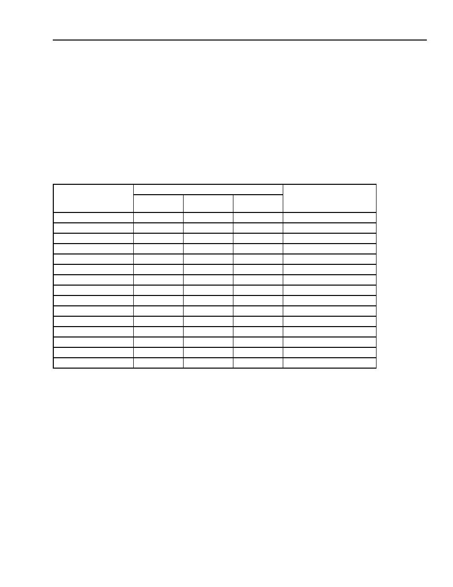
Data Sheet
June 1999
ORCA Series 2 FPGAs
Lucent Technologies Inc.
127
Package Thermal Characteristics
(continued)
FPGA Maximum Junction Temperature
Once the power dissipated by the FPGA has been determined (see the Estimating Power Dissipation section), the
maximum junction temperature of the FPGA can be found. This is needed to determine if speed derating of the
device from the 85 ∞C junction temperature used in all of the delay tables is needed. Using the maximum ambient
temperature, T
Amax
, and the power dissipated by the device, Q (expressed in ∞C), the maximum junction tempera-
ture is approximated by:
T
Jmax =
T
Amax
+ (Q ∑
JA
)
Table 29 lists the thermal characteristics for all packages used with the Series 2 FPGAs.
1. Mounted on a sparse copper one-layer test board.
2. Mounted on four-layer JEDEC standard test board with two power/ground planes.
3. With thermal balls connected to board ground plane.
4. Without thermal balls connected to board ground plane.
Note: The
JC
for the packages listed is <1 ∞C/W. This implies that virtually all of the heat is dissipated through the board on which the package
is mounted.
Table 29. Series 2 Plastic Package Thermal Guidelines
Package
JA
(∞C/W)
T
A
= 70 ∞C max
T
J
= 125 ∞C max
@ 0 fpm (W)
0 fpm
200 fpm
500 fpm
84-Pin PLCC
1
40.0
35.0
--
1.4
100-Pin TQFP
2
30.0--27.0
26--23
24.0--21.0
1.8--2.0
144-Pin TQFP
1
52.0
39.0
--
1.1
160-Pin QFP
2
24.0
21.5
20.5
2.3
208-Pin SQFP
2
26.5
23.0
21.0
2.1
208-Pin SQFP2
2
12.8
10.3
9.1
4.3
240-Pin SQFP
2
25.5
22.5
21.0
2.2
240-Pin SQFP2
2
13.0
10.0
9.0
4.2
256-Pin PBGA
2, 3
22.5
19.0
17.5
2.4
256-Pin PBGA
2, 4
26.0
22.0
20.5
2.1
304-Pin SQFP
2
27.5
24.0
22.5
2.0
304-Pin SQFP2
2
12.0
10.0
9.0
4.6
352-Pin PBGA
2, 3
19.0
16.0
15.0
2.9
352-Pin PBGA
2, 4
25.5
22.0
20.5
2.1
432-Pin EBGA
2
11.0
8.5
7.5
5.0
Package Coplanarity
The coplanarity limits of the Series 2
series packages
are as follows:
s
TQFP: 3.15 mils
s
PLCC and QFP: 4.0 mils
s
PBGA: 8.0 mils
s
SQFP: 4.0 mils (240 and 304 only)
3.15 mils (all other sizes)
s
SQFP2: 3.15 mils
s
EBGA: 8.0 mils
Package Parasitics
The electrical performance of an IC package, such as
signal quality and noise sensitivity, is directly affected
by the package parasitics. Table 30 lists eight parasitics
associated with the
ORCA
packages. These parasitics
represent the contributions of all components of a
package, which include the bond wires, all internal
package routing, and the external leads.
Four inductances in nH are listed: L
SW
and L
SL,
the
self-inductance of the lead; and L
MW
and L
ML
, the
mutual inductance to the nearest neighbor lead.

Data Sheet
ORCA Series 2 FPGAs
June 1999
128
Lucent Technologies Inc.
Package Parasitics
(continued)
These parameters are important in determining ground bounce noise and inductive crosstalk noise. Three capaci-
tances in pF are listed: C
M
, the mutual capacitance of the lead to the nearest neighbor lead; and C
1
and C
2
, the
total capacitance of the lead to all other leads (all other leads are assumed to be grounded). These parameters are
important in determining capacitive crosstalk and the capacitive loading effect of the lead.
The parasitic values in Table 30 are for the circuit model of bond wire and package lead parasitics. If the mutual
capacitance value is not used in the designer's model, then the value listed as mutual capacitance should be added
to each of the C
1
and C
2
capacitors.
5-3862(F).r2
Figure 53. Package Parasitics
Table 30. Series 2 Package Parasitics
Package Type
L
SW
L
MW
R
W
C
1
C
2
C
M
L
SL
L
ML
84-Pin PLCC
3
1
140
1
1
0.5
7--11
3--6
100-Pin TQFP
3
1
150
0.5
0.5
0.4
4--6
2--3
144-Pin TQFP
3
1
140
1
1
0.6
4--6
2--2.5
160-Pin QFP
4
1.5
180
1.5
1.5
1
10--13
6--8
208-Pin SQFP
4
2
200
1
1
1
7--10
4--6
208-Pin SQFP2
4
2
200
1
1
1
6--9
4--6
240-Pin SQFP
4
2
200
1
1
1
8--12
5--8
240-Pin SQFP2
4
2
200
1
1
1
7--11
4--7
256-Pin PBGA
5
2
220
1
1
1
5--8
2--4
304-Pin SQFP
5
2
220
1
1
1
12--18
7--12
304-Pin SQFP2
5
2
220
1
1
1
11--17
7--12
352-Pin PBGA
5
2
220
1.5
1.5
1.5
7--12
3--6
432-Pin EBGA
4
1.5
500
1
1
0.3
3--5.5
0.5--1
PAD N
CIRCUIT
BOARD PAD
C
M
C
1
L
W
R
W
L
L
L
MW
C
2
C
1
L
ML
C
2
PAD N + 1
L
W
R
W
L
L

Data Sheet
June 1999
ORCA Series 2 FPGAs
Lucent Technologies Inc.
129
Absolute Maximum Ratings
Stresses in excess of the absolute maximum ratings can cause permanent damage to the device. These are abso-
lute stress ratings only. Functional operation of the device is not implied at these or any other conditions in excess of
those given in the operations sections of this data sheet. Exposure to absolute maximum ratings for extended periods
can adversely affect device reliability.
The
ORCA
Series FPGAs include circuitry designed to protect the chips from damaging substrate injection currents
and prevent accumulations of static charge. Nevertheless, conventional precautions should be observed during stor-
age, handling, and use to avoid exposure to excessive electrical stress.
Recommended Operating Conditions
Notes:
During powerup and powerdown sequencing, V
DD
is allowed to be at a higher voltage level than V
DD
5 for up to 100 ms.
During powerup sequencing of OR2TxxA devices V
DD
should reach 1.0 V before voltage applied to V
DD
5 can be greater than the voltage applied
to V
DD.
The maximum recommended junction temperature (T
J
) during operation is 125 ∞C.
* V
DD
5 not used in OR2TxxB devices.
Parameter
Symbol
Min
Max
Unit
Storage Temperature
T
stg
≠65
150
∞C
Supply Voltage with Respect to Ground
V
DD
≠0.5
7.0
V
V
DD
5 Supply Voltage with Respect to Ground
(OR2TxxA)
V
DD
5
V
DD
7.0
V
Input Signal with Respect to Ground
OR2TxxA only
--
≠0.5
V
DD
+ 0.3
V
DD
5 + 0.3
V
Signal Applied to High-impedance Output
OR2TxxA only
--
≠0.5
V
DD
+ 0.3
V
DD
5 + 0.3
V
Maximum Soldering Temperature
--
--
260
∞C
Mode
OR2CxxA
OR2TxxA/OR2TxxB
Temperature
Range
(Ambient)
Supply Voltage
(V
DD
)
Temperature
Range
(Ambient)
Supply Voltage
(V
DD
)
Supply Voltage*
(V
DD
5)
Commercial
0 ∞C to 70 ∞C
5 V ± 5%
0 ∞C to 70 ∞C
3.0 V to 3.6 V
V
DD
to 5.25 V
Industrial
≠40 ∞C to +85 ∞C
5 V ± 10%
≠40 ∞C to +85 ∞C
3.0 V to 3.6 V
V
DD
to 5.25 V

Data Sheet
ORCA Series 2 FPGAs
June 1999
130
Lucent Technologies Inc.
Electrical Characteristics
* On the OR2TxxA devices, the pull-up resistor will externally pull the pin to a level 1.0 V below V
DD
.
Table 31A. OR2CxxA and OR2TxxA Electrical Characteristics
OR2CxxA Commercial: V
DD
= 5.0 V ± 5%, 0 ∞C
T
A
70 ∞C; OR2CxxA Industrial: V
DD
= 5.0 V ± 10%, ≠40 ∞C
T
A
+85 ∞C.
OR2TxxA Commercial: V
DD
= 3.0 V to 3.6 V, 0 ∞C
T
A
70 ∞C; OR2TxxA Industrial: V
DD
= 3.0 V to 3.6 V, ≠40 ∞C
T
A
+85
∞C.
Parameter
Sym-
bol
Test Conditions
OR2CxxA
OR2TxxA
Unit
Min
Max
Min
Max
Input Voltage:
High
Low
V
IH
V
IL
Input configured as CMOS
50% V
DD
GND ≠ 0.5
V
DD
+ 0.3
30% V
DD
50% V
DD5
GND ≠ 0.5
V
DD5
+ 0.3
30% V
DD5
V
V
Input Voltage:
High
Low
V
IH
V
IL
Input configured as TTL
(valid for OR2CxxA only)
2.0
≠0.5
V
DD
+ 0.3
0.8
--
--
--
--
V
V
Output Voltage:
High
Low
V
OH
V
OL
V
DD
=
min, I
OH
= 6 mA or 3 mA
V
DD
= min,
I
OL
= 12 mA or 6 mA
2.4
--
--
0.4
2.4
--
--
0.4
V
V
Input Leakage Current
I
L
V
DD
= Max, V
IN
= V
SS
or V
DD
≠10
10
≠10
10
µA
Standby Current:
OR2C04A/OR2T04A
OR2C06A/OR2T06A
OR2C08A/OR2T08A
OR2C10A/OR2T10A
OR2C12A/OR2T12A
OR2C15A/OR2T15A
OR2C26A/OR2T26A
OR2C40A/OR2T40A
I
DDSB
OR2CxxA (T
A
= 25 ∞C, V
DD
= 5.0 V)
OR2TxxA (T
A
= 25 ∞C, V
DD
= 3.3 V)
internal oscillator running,
no output loads,
inputs at V
DD
or GND
(after configuration)
--
--
--
--
--
--
--
--
6.5
7.0
7.7
8.4
9.2
10.0
12.2
16.3
--
--
--
--
--
--
--
--
4.0
4.3
4.8
5.3
5.8
6.3
7.8
10.6
mA
mA
mA
mA
mA
mA
mA
mA
Standby Current:
OR2C04A/OR2T04A
OR2C06A/OR2T06A
OR2C08A/OR2T08A
OR2C10A/OR2T10A
OR2C12A/OR2T12A
OR2C15A/OR2T15A
OR2C26A/OR2T26A
OR2C40A/OR2T40A
I
DDSB
OR2CxxA (T
A
= 25 ∞C, V
DD
= 5.0 V)
OR2TxxA (T
A
= 25 ∞C, V
DD
= 3.3 V)
internal oscillator stopped,
no output loads,
inputs at V
DD
or GND
(after configuration)
--
--
--
--
--
--
--
--
1.5
2.0
2.7
3.4
4.2
5.0
7.2
11.3
--
--
--
--
--
--
--
--
1.0
1.3
1.8
2.3
2.8
3.3
4.8
7.6
mA
mA
mA
mA
mA
mA
mA
mA
Data Retention Voltage
V
DR
T
A
= 25 ∞C
2.3
--
2.3
--
V
Input Capacitance
C
IN
OR2CxxA (T
A
= 25 ∞C, V
DD
= 5.0 V)
OR2TxxA (T
A
= 25 ∞C, V
DD
= 3.3 V)
Test frequency = 1 MHz
--
9
--
9
pF
Output Capacitance
C
OUT
OR2CxxA (T
A
= 25 ∞C, V
DD
= 5.0 V)
OR2TxxA (T
A
= 25 ∞C, V
DD
= 3.3 V)
Test frequency = 1 MHz
--
9
--
9
pF
DONE Pull-up Resistor*
R
DONE
--
100k
--
100k
--
M3, M2, M1, and M0
Pull-up Resistors*
R
M
--
100k
--
100k
--
I/O Pad Static Pull-up
Current*
I
PU
OR2CxxA (V
DD
= 5.25 V, V
IN
= V
SS
,
T
A
= 0 ∞C)
OR2TxxA (V
DD
= 3.6 V, V
IN
= V
SS
,
T
A
= 0 ∞C)
14.4
50.9
14.4
50.9
µA
I/O Pad Static Pull-down
Current
I
PD
OR2CxxA (V
DD
= 5.25 V, V
IN
= V
SS
,
T
A
= 0 ∞C)
OR2TxxA (V
DD
= 3.6 V, V
IN
= V
SS
,
T
A
= 0 ∞C)
26
103
26
103
µA
I/O Pad Pull-up Resistor*
R
PU
V
DD
= All, V
IN
= V
SS
, T
A
= 0 ∞C
100k
--
100k
--
I/O Pad Pull-down
Resistor
R
PD
V
DD
= All, V
IN
= V
DD
, T
A
= 0 ∞C
50k
--
50k
--

Data Sheet
June 1999
ORCA Series 2 FPGAs
Lucent Technologies Inc.
131
Electrical Characteristics
(continued)
* On the OR2TxxB devices, the pull-up resistor will externally pull the pin to a level 1.0 V below V
DD
.
Table 31B. OR2TxxB Electrical Characteristics
OR2TxxB Commercial: V
DD
= 3.0 V to 3.6 V, 0 ∞C
T
A
70 ∞C; OR2TxxB Industrial: V
DD
= 3.0 V to 3.6 V, ≠40 ∞C
T
A
+85
∞C.
Parameter
Symbol
Test Conditions
OR2TxxB
Unit
Min
Max
Input Voltage:
High
Low
V
IH
V
IL
Input configured as CMOS
80% V
DD
GND ≠ 0.5
V
DD
+ 0.3
15% V
DD
V
V
Output Voltage:
High
Low
V
OH
V
OL
V
DD
=
min, I
OH
= 6 mA or 3 mA
V
DD
= min,
I
OL
= 12 mA or 6 mA
2.4
--
--
0.4
V
V
Input Leakage Current
I
L
V
DD
= max, V
IN
= V
SS
or V
DD
≠10
10
µA
Standby Current:
OR2T15B
OR2T40B
I
DDSB
OR2TxxB (T
A
= 25 ∞C, V
DD
= 3.3 V)
internal oscillator running,
no output loads,
inputs at V
DD
or GND
(after configuration)
--
--
5.5
8.0
mA
mA
Standby Current:
OR2T15B
OR2T40B
I
DDSB
OR2TxxB (T
A
= 25 ∞C, V
DD
= 3.3 V)
internal oscillator stopped,
no output loads,
inputs at V
DD
or GND
(after configuration)
--
--
2.0
4.5
mA
mA
Data Retention Voltage
V
DR
T
A
= 25 ∞C
2.3
--
V
Input Capacitance
C
IN
OR2TxxB (T
A
= 25 ∞C, V
DD
= 3.3 V)
Test frequency = 1 MHz
--
8
pF
Output Capacitance
C
OUT
OR2TxxB (T
A
= 25 ∞C, V
DD
= 3.3 V)
Test frequency = 1 MHz
--
8
pF
DONE Pull-up Resistor*
R
DONE
--
100k
--
M3, M2, M1, and M0
Pull-up Resistors*
R
M
--
100k
--
I/O Pad Static Pull-up
Current*
I
PU
V
DD
= 3.6 V, V
IN
= V
SS
, T
A
= 0 ∞C
14.4
50.9
µA
I/O Pad Static Pull-down Cur-
rent
I
PD
V
DD
= 3.6 V, V
IN
= V
DD
, T
A
= 0 ∞C
26
103
µA
I/O Pad Pull-up Resistor*
R
PU
V
DD
= all, V
IN
= V
SS
, T
A
= 0 ∞C
100k
--
I/O Pad Pull-down
Resistor
R
PD
V
DD
= all, V
IN
= V
DD
, T
A
= 0 ∞C
50k
--
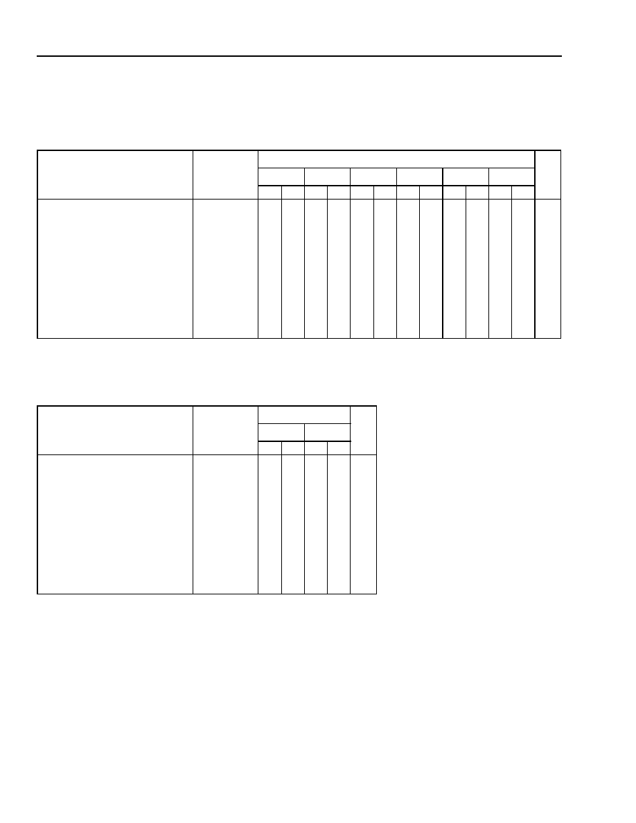
Data Sheet
ORCA Series 2 FPGAs
June 1999
132
Lucent Technologies Inc.
Timing Characteristics
Note: Speed grades of -5, -6, and -7 are for OR2TxxA devices only.
Table 32A. OR2CxxA and OR2TxxA Combinatorial PFU Timing Characteristics
OR2CxxA Commercial: V
DD
= 5.0 V ± 5%, 0 ∞C
T
A
70 ∞C; OR2CxxA Industrial: V
DD
= 5.0 V ± 10%, ≠40 ∞C
T
A
+85 ∞C.
OR2TxxA Commercial: V
DD
= 3.0 V to 3.6 V, 0 ∞C
T
A
70 ∞C; OR2TxxA Industrial: V
DD
= 3.0 V to 3.6 V, ≠40 ∞C
T
A
+85
∞C.
Parameter
Symbol
Speed
Unit
-2
-3
-4
-5
-6
-7
Min Max Min Max Min Max Min Max Min Max Min Max
Combinatorial Delays
(T
J
= +85 ∞C, V
DD
= min):
Four Input Variables (A[4:0],
B[4:0] to F[3:0])
Five Input Variables (A[4:0],
B[4:0] to F3, F0)
PFUMUX (A[4:0], B[4:0] to F1)
PFUMUX (C0 to f1)
PFUNAND (A[4:0], B[4:0] to F2)
PFUNAND (C0 to F2)
PFUXOR (A[4:0], B[4:0] to F1)
PFUXOR (C0 to F1)
F4*_DEL
F5*_DEL
MUX_DEL
C0MUX_DEL
ND_DEL
C0ND_DEL
XOR_DEL
C0XOR_DEL
--
--
--
--
--
--
--
--
4.0
4.1
4.7
3.0
4.7
2.7
5.6
3.1
--
--
--
--
--
--
--
--
2.8
2.9
3.8
2.2
4.0
2.2
4.5
2.2
--
--
--
--
--
--
--
--
2.1
2.2
3.2
1.9
3.3
1.8
3.8
2.0
--
--
--
--
--
--
--
--
1.7
1.8
2.6
1.5
2.7
1.5
3.1
1.6
--
--
--
--
--
--
--
--
1.4
1.4
1.9
1.1
1.8
1.0
2.3
1.1
--
--
--
--
--
--
--
--
1.3
1.3
1.8
1.0
1.7
0.8
2.1
1.0
ns
ns
ns
ns
ns
ns
ns
ns
Table 32B. OR2TxxB Combinatorial PFU Timing Characteristics
OR2TxxB Commercial: V
DD
= 3.0 V to 3.6 V, 0 ∞C
T
A
70 ∞C; OR2TxxB Industrial: V
DD
= 3.0 V to 3.6 V, ≠40 ∞C
T
A
+85
∞C.
Parameter
Symbol
Speed
Unit
-7
-8
Min Max Min Max
Combinatorial Delays
(T
J
= +85 ∞C, V
DD
= min):
Four Input Variables (A[4:0],
B[4:0] to F[3:0])
Five Input Variables (A[4:0],
B[4:0] to F3, F0)
PFUMUX (A[4:0], B[4:0] to F1)
PFUMUX (C0 to F1)
PFUNAND (A[4:0], B[4:0] to F2)
PFUNAND (C0 to F2)
PFUXOR (A[4:0], B[4:0] to F1)
PFUXOR (C0 to F1)
F4*_DEL
F5*_DEL
MUX_DEL
C0MUX_DEL
ND_DEL
C0ND_DEL
XOR_DEL
C0XOR_DEL
--
--
--
--
--
--
--
--
1.3
1.3
2.2
1.4
2.1
1.2
2.5
1.3
--
--
--
--
--
--
--
--
1.0
1.0
1.8
1.0
1.7
0.9
2.0
1.0
ns
ns
ns
ns
ns
ns
ns
ns

Data Sheet
June 1999
ORCA Series 2 FPGAs
Lucent Technologies Inc.
133
Timing Characteristics
(continued)
5-4633(F).a
C = controlled by configuration RAM.
Notes:
The parameters MUX_DEL, XOR_DEL, and ND_DEL include the delay through the LUT in F5A/F5B modes.
See Table 41 for an explanation of FDBK_DEL and OMUX_DEL.
Figure 54. Combinatorial PFU Timing
A[4:0], B[4:0]
A[4:0], B[4:0]
A[4:0], B[4:0]
F4*_DEL
(LUT)
PFU
4
F5*_DEL
(LUT)
2
(LUT)
2
C0
MUX_DEL
C
F[3:0]
F3, F0
F1
F2
O[4:0]
FDBK_DEL
XSW LINES
OUTPUT MUX
OM
UX
_
D
E
L
C0MUX_DEL, C0XOR_DEL, C0ND_DEL
XOR_DEL
ND_DEL

Data Sheet
ORCA Series 2 FPGAs
June 1999
134
Lucent Technologies Inc.
Timing Characteristics
(continued)
1.The input buffers contain a programmable delay to allow the hold time vs. the external clock pin to be equal to 0.
Note: Speed grades of -5, -6, and -7 are for OR2TxxA devices only.
Table 33A. OR2CxxA and OR2TxxA Sequential PFU Timing Characteristics
OR2CxxA Commercial: V
DD
= 5.0 V ± 5%, 0 ∞C
T
A
70 ∞C; OR2CxxA Industrial: V
DD
= 5.0 V ± 10%, ≠40 ∞C
T
A
+85 ∞C.
OR2TxxA Commercial: V
DD
= 3.0 V to 3.6 V, 0 ∞C
T
A
70 ∞C; OR2TxxA Industrial: V
DD
= 3.0 V to 3.6 V, ≠40 ∞C
T
A
+85
∞C.
Parameter
Symbol
Speed
Unit
-2
-3
-4
-5
-6
-7
Min
Max
Min
Max Min Max Min Max Min Max Min Max
Input Requirements
Clock Low Time
T
CL
3.2
--
2.5
--
2.0
--
1.8
--
1.7
--
1.6
--
ns
Clock High Time
T
CH
3.2
--
2.5
--
2.0
--
1.8
--
1.7
--
1.6
--
ns
Global S/R Pulse Width (GSRN)
T
RW
2.8
--
2.5
--
2.0
--
1.8
--
1.7
--
1.6
--
ns
Local S/R Pulse Width
T
PW
3.0
--
2.5
--
2.0
--
1.8
--
1.7
--
1.6
--
ns
Combinatorial Setup Times (T
J
= 85 ∞C,
V
DD
= min):
Four Input Variables to Clock
(A[4:0], B[4:0] to CK)
Five Input Variables to Clock
(A[4:0], B[4:0] to CK)
PFUMUX to Clock (A[4:0], B[4:0] to CK)
PFUMUX to Clock (C0 to CK)
PFUNAND to Clock (A[4:0], B[4:0] to CK)
PFUNAND to Clock (C0 to CK)
PFUXOR to Clock (A[4:0], B[4:0] to CK)
PFUXOR to Clock (C0 to CK)
Data In to Clock (WD[3:0] to CK)
Clock Enable to Clock (CE to CK)
Local Set/Reset (synchronous) (LSR to CK)
Data Select to Clock (SEL to CK)
Pad Direct In
F4*_SET
F5*_SET
MUX_SET
C0MUX_SET
ND_SET
C0ND_SET
XOR_SET
C0XOR_SET
D*_SET
CKEN_SET
LSR_SET
SELECT_SET
PDIN_SET
2.4
2.5
3.9
1.5
3.9
1.7
4.8
1.6
0.5
1.6
1.7
1.9
0.0
--
--
--
--
--
--
--
--
--
--
--
--
--
1.7
1.9
2.9
1.2
2.9
1.2
3.6
1.2
0.1
1.2
1.4
1.5
0.0
--
--
--
--
--
--
--
--
--
--
--
--
--
1.3
1.3
2.3
0.9
2.2
0.6
3.0
0.9
0.1
1.0
1.3
1.4
0.0
--
--
--
--
--
--
--
--
--
--
--
--
--
1.1
1.2
2.1
0.8
2.0
0.5
2.7
0.8
0.0
0.9
1.2
1.3
0.0
--
--
--
--
--
--
--
--
--
--
--
--
--
1.0
1.0
1.6
0.7
1.7
0.5
2.1
0.7
0.1
0.9
1.1
1.2
0.0
--
--
--
--
--
--
--
--
--
--
--
--
--
0.9
0.9
1.5
0.6
1.6
0.5
2.0
0.6
0.1
0.6
0.8
1.0
0.0
--
--
--
--
--
--
--
--
--
--
--
--
--
ns
ns
ns
ns
ns
ns
ns
ns
ns
ns
ns
ns
ns
Combinatorial Hold Times (T
J
= all, V
DD
= all):
Data In (WD[3:0] from CK)
Clock Enable (CE from CK)
Local Set/Reset (synchronous) (LSR from CK)
Data Select (sel from CK)
Pad Direct In Hold (DIA[3:0], DIB[3:0] to CK)
1
All Others
D*_HLD
CKEN_HLD
LSR_HLD
SELECT_HLD
PDIN_HLD
--
0.6
0.6
0.0
0.0
1.5
0.0
--
--
--
--
--
--
0.4
0.4
0.0
0.0
1.4
0.0
--
--
--
--
--
--
0.4
0.0
0.0
0.0
1.0
0.0
--
--
--
--
--
--
0.4
0.0
0.0
0.0
0.9
0.0
--
--
--
--
--
--
0.3
0.0
0.0
0.0
0.8
0.0
--
--
--
--
--
--
0.3
0.0
0.0
0.0
0.8
0.0
--
--
--
--
--
--
ns
ns
ns
ns
ns
ns
Output Characteristics
Sequential Delays (T
J
= 85 ∞C, V
DD
= min):
Local S/R (async) to PFU Out (LSR to Q[3:0])
Global S/R to PFU Out (GSRN to Q[3:0])
Clock to PFU Out (CK to Q[3:0])--Register
Clock to PFU Out (CK to Q[3:0])--Latch
Transparent Latch (WD[3:0] to Q[3:0])
LSR_DEL
GSR_DEL
REG_DEL
LTCH_DEL
LTCH_DDEL
--
--
--
--
--
4.5
2.9
2.4
2.5
3.5
--
--
--
--
--
3.4
2.3
2.0
2.0
2.7
--
--
--
--
--
3.1
2.0
1.9
1.9
2.5
--
--
--
--
--
2.5
1.6
1.5
1.5
2.0
--
--
--
--
--
2.0
1.3
1.3
1.3
2.0
--
--
--
--
--
1.6
1.2
1.0
1.0
1.8
ns
ns
ns
ns
ns

Data Sheet
June 1999
ORCA Series 2 FPGAs
Lucent Technologies Inc.
135
Timing Characteristics
(continued)
1.The input buffers contain a programmable delay to allow the hold time vs. the external clock pin to be equal to 0.
Table 33B. OR2TxxB Sequential PFU Timing Characteristics
OR2TxxB Commercial: V
DD
= 3.0 V to 3.6 V, 0 ∞C
T
A
70 ∞C; OR2TxxB Industrial: V
DD
= 3.0 V to 3.6 V, ≠40 ∞C
T
A
+85
∞C.
Parameter
Symbol
Speed
Unit
-7
-8
Min
Max
Min
Max
Input Requirements
Clock Low Time
T
CL
1.7
--
1.4
--
ns
Clock High Time
T
CH
1.7
--
1.4
--
ns
Global S/R Pulse Width (GSRN)
T
RW
1.7
--
1.4
--
ns
Local S/R Pulse Width
T
PW
1.7
--
1.4
--
ns
Combinatorial Setup Times (T
J
= 85 ∞C,
V
DD
= min):
Four Input Variables to Clock
(A[4:0], B[4:0] to CK)
Five Input Variables to Clock
(A[4:0], B[4:0] to CK)
PFUMUX to Clock (A[4:0], B[4:0] to CK)
PFUMUX to Clock (C0 to CK)
PFUNAND to Clock (A[4:0], B[4:0] to CK)
PFUNAND to Clock (C0 to CK)
PFUXOR to Clock (A[4:0], B[4:0] to CK)
PFUXOR to Clock (C0 to CK)
Data In to Clock (WD[3:0] to CK)
Clock Enable to Clock (CE to CK)
Local Set/Reset (synchronous) (LSR to CK)
Data Select to Clock (SEL to CK)
Pad Direct In
F4*_SET
F5*_SET
MUX_SET
C0MUX_SET
ND_SET
C0ND_SET
XOR_SET
C0XOR_SET
D*_SET
CKEN_SET
LSR_SET
SELECT_SET
PDIN_SET
1.0
1.0
1.3
1.1
1.0
0.8
1.3
1.1
0.2
1.0
1.0
1.0
0.0
--
--
--
--
--
--
--
--
--
--
--
--
--
0.8
0.8
1.3
0.8
0.8
0.7
1.3
0.8
0.1
0.8
0.8
0.8
0.0
--
--
--
--
--
--
--
--
--
--
--
--
--
ns
ns
ns
ns
ns
ns
ns
ns
ns
ns
ns
ns
ns
Combinatorial Hold Times (T
J
= all, V
DD
= all):
Data In (WD[3:0] from CK)
Clock Enable (CE from CK)
Local Set/Reset (synchronous) (LSR from CK)
Data Select (SEL from CK)
Pad Direct In Hold (DIA[3:0], DIB[3:0] to CK)
1
All Others
D*_HLD
CKEN_HLD
LSR_HLD
SELECT_HLD
PDIN_HLD
--
0.0
0.0
0.0
0.0
0.1
0.0
--
--
--
--
--
--
0.0
0.0
0.0
0.0
0.1
0.0
--
--
--
--
--
--
ns
ns
ns
ns
ns
ns
Output Characteristics
Sequential Delays (T
J
= 85 ∞C, V
DD
= min):
Local S/R (async) to PFU Out (LSR to Q[3:0])
Global S/R to PFU Out (GSRN to Q[3:0])
Clock to PFU Out (CK to Q[3:0])--Register
Clock to PFU Out (CK to Q[3:0])--Latch
Transparent Latch (WD[3:0] to Q[3:0])
LSR_DEL
GSR_DEL
REG_DEL
LTCH_DEL
LTCH_DDEL
2.2
1.4
1.0
1.0
1.7
--
--
--
--
--
1.8
1.0
1.0
1.0
1.4
--
--
--
--
--
ns
ns
ns
ns
ns

Data Sheet
ORCA Series 2 FPGAs
June 1999
136
Lucent Technologies Inc.
Timing Characteristics
(continued)
Table 34A. OR2CxxA and OR2TxxA Ripple Mode PFU Timing Characteristics
OR2CxxA Commercial: V
DD
= 5.0 V ± 5%, 0 ∞C
T
A
70 ∞C; OR2CxxA Industrial: V
DD
= 5.0 V ± 10%, ≠40 ∞C
T
A
+85 ∞C.
OR2TxxA Commercial: V
DD
= 3.0 V to 3.6 V, 0 ∞C
T
A
70 ∞C; OR2TxxA Industrial: V
DD
= 3.0 V to 3.6 V, ≠40 ∞C
T
A
+85
∞C.
Parameter
Symbol
Speed
Unit
-2
-3
-4
-5
-6
-7
Min
Max
Min
Max
Min
Max
Min
Max
Min
Max
Min
Max
Ripple Setup Times
(T
J
= +85 ∞C, V
DD
= min):
Operands to Clock (A[3:0], B[3:0] to CK)
Bitwise Operands to Clock
(A[i], B[i] to CK at F[i])
Carry-in from Fast Carry to Clock
(CIN to CK)
Carry-in from General Routing to Clock
(B4 to CK)
Add/Subtract to Clock (A4 to CK)
RIP_SET
FRIP_SET
CIN_SET
B4_SET
AS_SET
6.7
2.4
4.0
4.0
8.2
--
--
--
--
--
5.0
1.7
3.2
3.2
5.6
--
--
--
--
--
3.7
1.3
1.9
1.9
4.3
--
--
--
--
--
3.3
1.2
1.7
1.7
3.9
--
--
--
--
--
2.8
1.0
1.4
1.4
3.2
--
--
--
--
--
2.5
0.9
1.3
1.3
3.1
--
--
--
--
--
ns
ns
ns
ns
ns
Ripple Hold Times (T
J
= all, V
DD
= all): All
TH
0.0
--
0.0
--
0.0
--
0.0
--
0.0
--
0.0
--
ns
Ripple Delays (T
J
= 85 ∞C, V
DD
= min):
Operands to Carry-out (A[3:0], B[3:0]
to COUT)
Operands to Carry-out (A[3:0], B[3:0]
to O4)
Operands to PFU Out (A[3:0], B[3:0]
to F[3:0])
Bitwise Operands to PFU Out (A[i], B[i]
to F[i])
Carry-in from Fast Carry to Carry-out
(CIN to COUT)
Carry-in from Fast Carry to Carry-out
(CIN to O4)
Carry-in from Fast Carry to PFU Out
(CIN to F[3:0])
Carry-in from General Routing to Carry-
out (B4 to COUT)
Carry-in from General Routing to Carry-
out (B4 to O4)
Carry-in from General Routing to PFU Out
(B4 to F[3:0])
Add/Subtract to Carry-out (A4 to COUT)
Add/Subtract to Carry-out (A4 to O4)
Add/Subtract to PFU Out (A4 to F[3:0])
RIP_CODEL
RIP_O4DEL
RIP_DEL
FRIP_DEL
CIN_CODEL
CIN_O4DEL
CIN_DEL
B4_CODEL
B4_O4DEL
B4_DEL
AS_CODEL
AS_O4DEL
AS_DEL
--
--
--
--
--
--
--
--
--
--
--
--
--
5.4
6.9
8.2
4.0
1.9
3.5
5.6
1.9
3.5
5.6
6.1
7.6
9.7
--
--
--
--
--
--
--
--
--
--
--
--
--
3.8
4.8
6.0
2.8
1.6
2.6
4.2
1.6
2.6
4.2
4.5
5.6
6.8
--
--
--
--
--
--
--
--
--
--
--
--
--
3.3
4.2
4.7
2.1
1.1
2.1
2.9
1.1
2.1
2.9
3.9
4.9
5.3
--
--
--
--
--
--
--
--
--
--
--
--
--
2.6
3.4
3.8
1.7
0.9
1.7
2.3
0.9
1.7
2.3
3.1
3.9
4.3
--
--
--
--
--
--
--
--
--
--
--
--
--
2.1
2.6
3.2
1.6
0.7
1.3
2.2
0.7
1.3
2.2
2.5
3.1
3.5
--
--
--
--
--
--
--
--
--
--
--
--
--
1.8
2.4
2.8
1.5
0.6
1.1
1.7
0.6
1.1
2.1
2.3
2.8
3.1
ns
ns
ns
ns
ns
ns
ns
ns
ns
ns
ns
ns
ns
Notes:
The new 4 x 1 multiplier and 4-bit comparator submodes use the appropriate ripple mode timing shown above.
Speed grades of -5, -6, and -7 are for OR2TxxA devices only.

Data Sheet
June 1999
ORCA Series 2 FPGAs
Lucent Technologies Inc.
137
Timing Characteristics
(continued)
Table 34B. OR2TxxB Ripple Mode PFU Timing Characteristics
OR2TxxB Commercial: V
DD
= 3.0 V to 3.6 V, 0 ∞C
T
A
70 ∞C; OR2TxxB Industrial: V
DD
= 3.0 V to 3.6 V, ≠40 ∞C
T
A
+85
∞C.
Parameter
Symbol
Speed
Unit
-7
-8
Min
Max
Min
Max
Ripple Setup Times
(T
J
= 85 ∞C, V
DD
= min):
Operands to Clock (A[3:0], B[3:0] to CK)
Bitwise Operands to Clock
(A[i], B[i] to CK at F[i])
Carry-in from Fast Carry to Clock
(CIN to CK)
Carry-in from General Routing to Clock
(B4 to CK)
Add/Subtract to Clock (A4 to CK)
RIP_SET
FRIP_SET
CIN_SET
B4_SET
AS_SET
2.4
1.1
1.6
1.0
2.9
--
--
--
--
--
1.9
0.9
1.3
0.8
2.3
--
--
--
--
--
ns
ns
ns
ns
ns
Ripple Hold Times (T
J
= all, V
DD
= all): All
TH
ns
Ripple Delays (T
J
= 85 ∞C, V
DD
= min):
Operands to Carry-out (A[3:0], B[3:0]
to COUT)
Operands to Carry-out (A[3:0], B[3:0]
to O4)
Operands to PFU Out (A[3:0], B[3:0]
to F[3:0])
Bitwise Operands to PFU Out (A[i], B[i]
to F[i])
Carry-in from Fast Carry to Carry-out
(CIN to COUT)
Carry-in from Fast Carry to Carry-out
(CIN to O4)
Carry-in from Fast Carry to PFU Out
(CIN to F[3:0])
Carry-in from General Routing to Carry-
out (B4 to COUT)
Carry-in from General Routing to Carry-
out (B4 to O4)
Carry-in from General Routing to PFU Out
(B4 to F[3:0])
Add/Subtract to Carry-out (A4 to COUT)
Add/Subtract to Carry-out (A4 to O4)
Add/Subtract to PFU Out (A4 to F[3:0])
RIP_CODEL
RIP_O4DEL
RIP_DEL
FRIP_DEL
CIN_CODEL
CIN_O4DEL
CIN_DEL
B4_CODEL
B4_O4DEL
B4_DEL
AS_CODEL
AS_O4DEL
AS_DEL
2.2
3.0
3.1
1.4
0.7
1.4
1.9
0.7
1.4
1.9
2.7
3.4
3.6
--
--
--
--
--
--
--
--
--
--
--
--
--
1.8
2.4
2.5
1.1
0.6
1.2
1.5
0.6
1.2
1.5
2.2
2.8
2.9
--
--
--
--
--
--
--
--
--
--
--
--
--
ns
ns
ns
ns
ns
ns
ns
ns
ns
ns
ns
ns
ns
Notes: The new 4 x 1 multiplier and 4-bit comparator submodes use the appropriate ripple mode timing shown above.

Data Sheet
ORCA Series 2 FPGAs
June 1999
138
Lucent Technologies Inc.
Timing Characteristics
(continued)
Note: Speed grades of -5, -6, and -7 are for OR2TxxA devices only.
5-3226(F).r4
Figure 55. Read Operation--Flip-Flop Bypass
5-3227(F).r4
Figure 56. Read Operation--LUT Memory Loading Flip-Flops
Table 35A. OR2CxxA and OR2TxxA Asynchronous Memory Read Characteristics (MA/MB Modes)
OR2CxxA Commercial: V
DD
= 5.0 V ± 5%, 0 ∞C
T
A
70 ∞C; OR2CxxA Industrial: V
DD
= 5.0 V ± 10%, ≠40 ∞C
T
A
+85 ∞C.
OR2TxxA Commercial: V
DD
= 3.0 V to 3.6 V, 0 ∞C
T
A
70 ∞C; OR2TxxA Industrial: V
DD
= 3.0 V to 3.6 V, ≠40 ∞C
T
A
+85
∞C.
Parameter
Symbol
Speed
Unit
-2
-3
-4
-5
-6
-7
Min Max Min Max Min Max Min Max Min Max Min Max
Read Operation (T
J
= 85 ∞C, V
DD
= min):
Read Cycle Time
Data Valid after Address (A[3:0], B[3:0] to F[3:0])
T
RC
MEM*_ADEL
5.1
--
--
4.0
3.6
--
--
2.8
2.7
--
--
2.1
2.4
--
--
1.7
2.3
--
--
1.4
2.0
--
--
1.3
ns
ns
Read Operation, Clocking Data into Latch/Flip-flop
(T
J
= 85 ∞C, V
DD
= min):
Address to Clock Setup Time (A[3:0], B[3:0] to CK)
Clock to PFU Out (CK to Q[3:0])--Register
MEM*_ASET
REG_DEL
2.4
--
--
2.4
1.8
--
--
2.0
1.2
--
--
1.9
1.1
--
--
1.5
1.0
--
--
1.3
1.0
--
--
1.0
ns
ns
Table 35B. OR2TxxB Asynchronous Memory Read Characteristics (MA/MB Modes)
OR2TxxB Commercial: V
DD
= 3.0 V to 3.6 V, 0 ∞C
T
A
70 ∞C; OR2TxxB Industrial: V
DD
= 3.0 V to 3.6 V, ≠40 ∞C
T
A
+85
∞C.
Parameter
Symbol
Speed
Unit
-7
-8
Min
Max
Min
Max
Read Operation (T
J
= 85 ∞C, V
DD
= min):
Read Cycle Time
Data Valid after Address (A[3:0], B[3:0] to F[3:0])
T
RC
MEM*_ADEL
1.9
--
--
1.3
1.8
--
--
1.0
ns
ns
Read Operation, Clocking Data into Latch/Flip-flop
(T
J
= 85 ∞C, V
DD
= min):
Address to Clock Setup Time (A[3:0], B[3:0] to CK)
Clock to PFU Out (CK to Q[3:0])--Register
MEM*_ASET
REG_DEL
0.9
--
--
1.0
0.8
--
--
1.0
ns
ns
A[3:0], B[3:0]
F[3:0]
MEM*_ADEL
T
RC
A[3:0], B[3:0]
CK
MEM*_ASET
REG_DEL
Q[3:0]
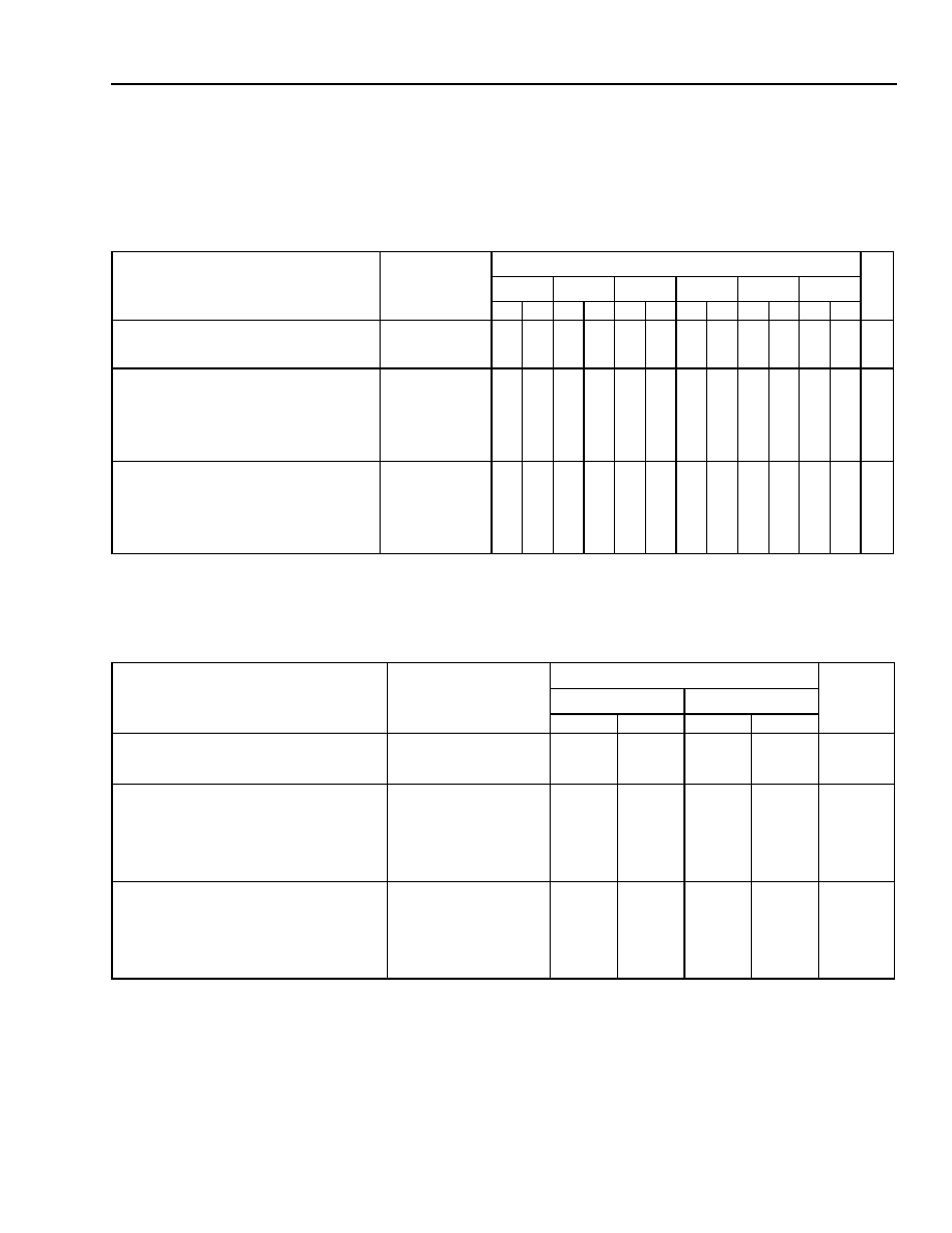
Data Sheet
June 1999
ORCA Series 2 FPGAs
Lucent Technologies Inc.
139
Timing Characteristics
(continued)
Note: Speed grades of -5, -6, and -7 are for OR2TxxA devices only.
Table 36A. OR2CxxA and OR2TxxA Asynchronous Memory Write Characteristics (MA/MB Modes)
OR2CxxA Commercial: V
DD
= 5.0 V ± 5%, 0 ∞C
T
A
70 ∞C; OR2CxxA Industrial: V
DD
= 5.0 V ± 10%, ≠40 ∞C
T
A
+85 ∞C.
OR2TxxA Commercial: V
DD
= 3.0 V to 3.6 V, 0 ∞C
T
A
70 ∞C; OR2TxxA Industrial: V
DD
= 3.0 V to 3.6 V, ≠40 ∞C
T
A
+85
∞C.
Parameter
Symbol
Speed
Unit
-2
-3
-4
-5
-6
-7
Min Max Min Max Min Max Min Max Min Max Min Max
Write Operation (TJ = 85 ∞C, VDD = min):
Write Cycle Time
Write Enable (WREN) Pulse Width (A4/B4)
TWC
TPW
9.3
3.0
--
--
7.8
2.5
--
--
6.3
2.0
--
--
5.7
1.8
--
--
5.2
1.7
--
--
5.1
1.6
--
--
ns
ns
Setup Time (TJ = 85 ∞C, VDD = min):
Address to WREN (A[3:0]/B[3:0] to A4/B4)
Data to WREN (WD[3:0] to A4/B4)
Address to WPE (A[3:0]/B[3:0] to C0)
Data to WPE (WD[3:0] to C0)
WPE to WREN (C0 to A4/B4)
MEM*_AWRSET
MEM*_DWRSET
MEM*_APWRSET
MEM*_DPWRSET
MEM*_WPESET
0.1
0.0
0.0
0.0
2.5
--
--
--
--
--
0.1
0.0
0.0
0.0
2.0
--
--
--
--
--
0.0
0.0
0.0
0.0
1.5
--
--
--
--
--
0.0
0.0
0.0
0.0
1.4
--
--
--
--
--
0.0
0.0
0.0
0.0
1.1
--
--
--
--
--
0.0
0.0
0.0
0.0
1.1
--
--
--
--
--
ns
ns
ns
ns
ns
Hold Time (TJ = all, VDD = all):
Address from WREN (A[3:0]/B[3:0] from A4/B4)
Data from WREN (WD[3:0] from A4/B4)
Address from WPE (A[3:0/B[3:0] to C0)
Data from WPE (WD[3:0] to C0)
WPE from WREN (C0 from A4/B4)
MEM*_WRAHLD
MEM*_WRDHLD
MEM*_PWRAHLD
MEM*_PWRDHLD
MEM*_WPEHLD
2.4
2.4
3.8
3.9
0.0
--
--
--
--
--
1.7
2.0
3.3
3.4
0.0
--
--
--
--
--
1.8
1.9
2.8
2.9
0.0
--
--
--
--
--
1.6
1.5
2.5
2.6
0.0
--
--
--
--
--
1.6
1.6
2.4
2.4
0.0
--
--
--
--
--
1.5
1.6
2.3
2.3
0.0
--
--
--
--
--
ns
ns
ns
ns
ns
Table 36B. OR2TxxB Asynchronous Memory Write Characteristics (MA/MB Modes)
OR2TxxB Commercial: V
DD
= 3.0 V to 3.6 V, 0 ∞C
T
A
70 ∞C; OR2TxxB Industrial: V
DD
= 3.0 V to 3.6 V, ≠40 ∞C
T
A
+85
∞C.
Parameter
Symbol
Speed
Unit
-7
-8
Min
Max
Min
Max
Write Operation (T
J
= 85 ∞C, V
DD
= min):
Write Cycle Time
Write Enable (WREN) Pulse Width (A4/B4)
T
WC
T
PW
5.1
1.7
--
--
4.2
1.4
--
--
ns
ns
Setup Time (T
J
= 85 ∞C, V
DD
= min):
Address to WREN (A[3:0]/B[3:0] to A4/B4)
Data to WREN (WD[3:0] to A4/B4)
Address to WPE (A[3:0]/B[3:0] to C0)
Data to WPE (WD[3:0] to C0)
WPE to WREN (C0 to A4/B4)
MEM*_AWRSET
MEM*_DWRSET
MEM*_APWRSET
MEM*_DPWRSET
MEM*_WPESET
0.0
0.0
0.0
0.0
1.0
--
--
--
--
--
0.0
0.0
0.0
0.0
0.8
--
--
--
--
--
ns
ns
ns
ns
ns
Hold Time (T
J
= all, V
DD
= all):
Address from WREN (A[3:0]/B[3:0] from A4/B4)
Data from WREN (WD[3:0] from A4/B4)
Address from WPE (A[3:0/B[3:0] to C0)
Data from WPE (WD[3:0] to C0)
WPE from WREN (C0 from A4/B4)
MEM*_WRAHLD
MEM*_WRDHLD
MEM*_PWRAHLD
MEM*_PWRDHLD
MEM*_WPEHLD
0.9
1.6
2.3
2.3
0.0
--
--
--
--
--
0.7
1.3
1.9
1.9
0.0
--
--
--
--
--
ns
ns
ns
ns
ns

Data Sheet
ORCA Series 2 FPGAs
June 1999
140
Lucent Technologies Inc.
Timing Characteristics
(continued)
5-3228(F).r6
Figure 57. Write Operation
A[3:0], B[3:0]
WD[3:0]
MEM*_APWRSET
T
WC
C0 (WPE)
MEM*_PWRAHLD
MEM*_WPEHLD
T
PW
MEM*_WPESET
A4, B4 (WREN)
MEM*_WRAHLD
MEM*_PWRDHLD
MEM*_DPWRSET
MEM*_AWRSET
MEM*_DWRSET
MEM*_WRDHLD
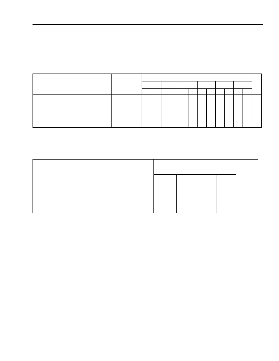
Data Sheet
June 1999
ORCA Series 2 FPGAs
Lucent Technologies Inc.
141
Timing Characteristics
(continued)
Note: Speed grades of -5, -6, and -7 are for OR2TxxA devices only.
Table 37A. OR2CxxA and OR2TxxA Asynchronous Memory Read During Write Operation (MA/MB Modes)
OR2CxxA Commercial: V
DD
= 5.0 V ± 5%, 0 ∞C
T
A
70 ∞C; OR2CxxA Industrial: V
DD
= 5.0 V ± 10%, ≠40 ∞C
T
A
+85 ∞C.
OR2TxxA Commercial: V
DD
= 3.0 V to 3.6 V, 0 ∞C
T
A
70 ∞C; OR2TxxA Industrial: V
DD
= 3.0 V to 3.6 V, ≠40 ∞C
T
A
+85
∞C.
Parameter
Symbol
Speed
Unit
-2
-3
-4
-5
-6
-7
Min Max Min Max Min Max Min Max Min Max Min Max
Read During Write Operation
(T
J
= 85 ∞C, V
DD
= min):
Write Enable (WREN) to PFU Output Delay
(A4/B4 to F[3:0])
Write-port Enable (WPE) to PFU Output
Delay (C0 to F[3:0])
Data to PFU Output Delay (WD[3:0] to F[3:0])
MEM*_WRDEL
MEM*_PWRDEL
MEM*_DDEL
--
--
--
7.0
9.0
5.0
--
--
--
4.9
6.4
3.6
--
--
--
4.8
5.8
3.1
--
--
--
3.9
4.7
2.5
--
--
--
4.0
4.7
2.5
--
--
--
3.9
4.5
2.2
ns
ns
ns
Table 37B. OR2TxxB Asynchronous Memory Read During Write Operation (MA/MB Modes)
OR2TxxB Commercial: V
DD
= 3.0 V to 3.6 V, 0 ∞C
T
A
70 ∞C; OR2TxxB Industrial: V
DD
= 3.0 V to 3.6 V, ≠40 ∞C
T
A
+85
∞C.
Parameter
Symbol
Speed
Unit
-7
-8
Min
Max
Min
Max
Read During Write Operation
(T
J
= +85 ∞C, V
DD
= min):
Write Enable (WREN) to PFU Output Delay
(A4/B4 to F[3:0])
Write-port Enable (WPE) to PFU Output
Delay (C0 to F[3:0])
Data to PFU Output Delay (WD[3:0] to F[3:0])
MEM*_WRDEL
MEM*_PWRDEL
MEM*_DDEL
--
--
--
4.5
4.6
2.7
--
--
--
3.9
4.0
2.4
ns
ns
ns

Data Sheet
ORCA Series 2 FPGAs
June 1999
142
Lucent Technologies Inc.
Timing Characteristics
(continued)
5-3229(F).r6
Figure 58. Read During Write
A[3:0], B[3:0]
A4, B4 (WREN)
WD[3:0]
F[3:0]
WD[3:0]
F[3:0]
T
PW
MEM*_WRDEL
MEM*_DDEL
MEM*_WRDEL
DATA STABLE
DURING
WREN AND WPE
DATA CHANGING
DURING
WREN AND WPE
CO (WPE)
MEM*_PWRDEL
MEM*_PWRDEL
Data Sheet
June 1999
ORCA Series 2 FPGAs
Lucent Technologies Inc.
143
Timing Characteristics
(continued)
Note: Speed grades of -5, -6, and -7 are for OR2TxxA devices only.
Table 38A. OR2CxxA and OR2TxxA Asynchronous Memory Read During Write, Clocking Data into Latch/
Flip-Flop (MA/MB Modes)
OR2CxxA Commercial: V
DD
= 5.0 V ± 5%, 0 ∞C
T
A
70 ∞C; OR2CxxA Industrial: V
DD
= 5.0 V ± 10%, ≠40 ∞C
T
A
+85 ∞C.
OR2TxxA Commercial: V
DD
= 3.0 V to 3.6 V, 0 ∞C
T
A
70 ∞C; OR2TxxA Industrial: V
DD
= 3.0 V to 3.6 V, ≠40 ∞C
T
A
+85
∞C.
Parameter
Symbol
Speed
Unit
-2
-3
-4
-5
-6
-7
Min Max
Min Max Min Max Min Max Min Max Min Max
Setup Time (TJ = 85 ∞C, V
DD
= min):
Address to Clock (A[3:0], B[3:0] to CK)
Write Enable (WREN) to Clock (A4/B4 to CK)
Write-port Enable (WPE) to Clock (C0 to CK)
Data (WD[3:0] to CK)
MEM*_ASET
MEM*_WRSET
MEM*_PWRSET
MEM*_DSET
2.4
5.4
7.4
3.5
--
--
--
--
1.8
4.4
5.9
2.6
--
--
--
--
1.2
3.8
4.8
2.6
--
--
--
--
1.1
3.4
4.3
2.3
--
--
--
--
1.0
3.1
4.0
2.2
--
--
--
--
1.0
3.0
3.9
2.1
--
--
--
--
ns
ns
ns
ns
Hold Time (TJ = All, V
DD
= All): All
TH
0.0
--
0.0
--
0.0
--
0.0
--
0.0
--
0.0
--
ns
Clock to PFU Out (CK to Q[3:0])--Register
REG_DEL
--
2.4
--
2.0
--
1.9
--
1.5
--
1.3
--
1.0
ns
Table 38B. OR2TxxB Asynchronous Memory Read During Write, Clocking Data into Latch/Flip-Flop
(MA/MB Modes)
OR2TxxB Commercial: V
DD
= 3.0 V to 3.6 V, 0 ∞C
T
A
70 ∞C; OR2TxxB Industrial: V
DD
= 3.0 V to 3.6 V, ≠40 ∞C
T
A
+85
∞C.
Parameter
Symbol
Speed
Unit
-7
-8
Min
Max
Min
Max
Setup Time (T
J
= 85 ∞C, V
DD
= min):
Address to Clock (A[3:0], B[3:0] to CK)
Write Enable (WREN) to Clock (A4/B4 to CK)
Write-port Enable (WPE) to Clock (C0 to CK)
Data (WD[3:0] to CK)
MEM*_ASET
MEM*_WRSET
MEM*_PWRSET
MEM*_DSET
0.9
2.9
3.7
2.0
--
--
--
--
0.8
2.5
3.2
1.7
--
--
--
--
ns
ns
ns
ns
Hold Time (T
J
= all, V
DD
= all): All
TH
0.0
--
0.0
--
ns
Clock to PFU Out (CK to Q[3:0])--Register
REG_DEL
--
1.0
--
1.0
ns

Data Sheet
ORCA Series 2 FPGAs
June 1999
144
Lucent Technologies Inc.
Timing Characteristics
(continued)
5-3230(F).r6
Figure 59. Read During Write--Clocking Data into Flip-Flop
A[3:0], B[3:0]
A4, B4 (WREN)
WD[3:0]
CK
T
PW
MEM*_DSET
Q[3:0]
MEM*_ASET
REG_DEL
C0 (WPE)
MEM*_PWRSET
MEM*_WRSET

Data Sheet
June 1999
ORCA Series 2 FPGAs
Lucent Technologies Inc.
145
Timing Characteristics
(continued)
1. Readback of the configuration bit stream when simultaneously writing to a PFU in either SSPM fast mode or SDPM fast mode is not allowed.
2. Because the setup time of data into the latches/FFs is less than 0 ns, data written into the RAM can be loaded into a latch/FF in the same
PFU on the next opposite clock edge (one-half clock period).
Note: Speed grades of -5, -6, and -7 are for OR2TxxA devices only.
Table 39A. OR2CxxA and OR2TxxA Synchronous Memory Write Characteristics (SSPM and SDPM Modes)
OR2CxxA Commercial: V
DD
= 5.0 V ± 5%, 0 ∞C
T
A
70 ∞C; OR2CxxA Industrial: V
DD
= 5.0 V ± 10%, ≠40 ∞C
T
A
+85 ∞C.
OR2TxxA Commercial: V
DD
= 3.0 V to 3.6 V, 0 ∞C
T
A
70 ∞C; OR2TxxA Industrial: V
DD
= 3.0 V to 3.6 V, ≠40 ∞C
T
A
+85
∞C.
Parameter
Symbol
Speed
Unit
-2
-3
-4
-5
-6
-7
Min
Max
Min
Max
Min
Max
Min
Max
Min
Max
Min
Max
Write Operation for Fast-RAM Mode
1
:
Maximum Frequency
Clock Low Time
Clock High Time
Clock to Data Valid (CK to F[3:0])
2
FFSCK
TFSCL
TFSCH
FMEMS_DEL
38.2
13.1
13.1
--
--
--
--
9.0
52.6
9.5
9.5
--
--
--
--
7.4
83.3
6.0
6.0
--
--
--
--
6.2
90.9
5.5
5.5
--
--
--
--
5.0
92.6
5.4
5.4
--
--
--
--
5.3
96.2
5.2
5.2
--
--
--
--
5.2
MHz
ns
ns
ns
Write Operation for Normal RAM Mode:
Maximum Frequency
Clock Low Time
Clock High Time
Clock to Data Valid (CK to F[3:0])
FSCK
TSCL
TSCH
MEMS_DEL
24.3
20.6
20.6
--
--
--
--
10.9
33.3
15.0
15.0
--
--
--
--
8.6
52.6
9.5
9.5
--
--
--
--
7.5
58.0
8.5
8.5
--
--
--
--
6.0
58.8
8.5
8.5
--
--
--
--
6.4
59.8
8.4
8.4
--
--
--
--
5.9
MHz
ns
ns
ns
Write Operation Setup Time:
Address to Clock (A[3:0]/B[3:0] to CK)
Data to Clock (WD[3:0] to CK)
Write Enable (WREN) to Clock
(A4 to CK)
Write-port Enable (WPE) to Clock
(C0 to CK)
MEMS_ASET
MEMS_DSET
MEMS_WRSET
MEMS_PWRSET
0.0
0.0
0.0
0.0
--
--
--
--
0.0
0.0
0.0
0.0
--
--
--
--
0.0
0.0
0.0
0.0
--
--
--
--
0.0
0.0
0.0
0.0
--
--
--
--
0.0
0.0
0.0
0.0
--
--
--
--
0.0
0.0
0.0
0.0
--
--
--
--
ns
ns
ns
ns
Write Operation Hold Time:
Address to Clock (A[3:0]/B[3:0] to CK)
Data to Clock (WD[3:0] to CK)
Write Enable (WREN) to Clock
(A4 to CK)
Write-port Enable (WPE) to Clock
(C0 to CK)
MEMS_AHLD
MEMS_DHLD
MEMS_WRHLD
MEMS_PWRHLD
3.8
3.8
3.8
3.3
--
--
--
--
3.0
3.0
3.0
2.3
--
--
--
--
2.2
2.2
2.2
1.5
--
--
--
--
2.0
2.0
2.0
1.4
--
--
--
--
1.9
1.9
1.9
1.9
--
--
--
--
1.8
1.8
1.8
1.2
--
--
--
--
ns
ns
ns
ns
Table 39.B OR2TxxB Synchronous Memory Write Characteristics (SSPM and SDPM Modes)
OR2TxxB Commercial: V
DD
= 3.0 V to 3.6 V, 0 ∞C
T
A
70 ∞C; OR2TxxB Industrial: V
DD
= 3.0 V to 3.6 V, ≠40 ∞C
T
A
+85
∞C.
Parameter
Symbol
Speed
Unit
-7
-8
Min
Max
Min
Max
Write Operation for Fast-RAM Mode
1
:
Maximum Frequency
Clock Low Time
Clock High Time
Clock to Data Valid (CK to F[3:0])
2
F
FSCK
T
FSCL
T
FSCH
FMEMS_DEL
97.7
5.1
5.1
--
--
--
--
5.1
112.4
4.5
4.5
--
--
--
--
4.5
MHz
ns
ns
ns
Write Operation for Normal RAM Mode:
Maximum Frequency
Clock Low Time
Clock High Time
Clock to Data Valid (CK to F[3:0])
F
SCK
T
SCL
T
SCH
MEMS_DEL
60.8
8.2
8.2
--
--
--
--
5.1
69.9
7.2
7.2
--
--
--
--
4.5
MHz
ns
ns
ns
Data Sheet
ORCA Series 2 FPGAs
June 1999
146
Lucent Technologies Inc.
1. Readback of the configuration bit stream when simultaneously writing to a PFU in either SSPM fast mode or SDPM fast mode is not allowed.
2. Because the setup time of data into the latches/FFs is less than 0 ns, data written into the RAM can be loaded into a latch/FF in the same
PFU on the next opposite clock edge (one-half clock period).
Note: Speed grades of -5, -6, and -7 are for OR2TxxA devices only.
5-4621(F).a
Figure 60. Synchronous Memory Write Characteristics
Write Operation Setup Time:
Address to Clock (A[3:0]/B[3:0] to CK)
Data to Clock (WD[3:0] to CK)
Write Enable (WREN) to Clock
(A4 to CK)
Write-port Enable (WPE) to Clock
(C0 to CK)
MEMS_ASET
MEMS_DSET
MEMS_WRSET
MEMS_PWRSET
0.0
0.0
0.0
0.0
--
--
--
--
0.0
0.0
0.0
0.0
--
--
--
--
ns
ns
ns
ns
Write Operation Hold Time:
Address to Clock (A[3:0]/B[3:0] to CK)
Data to Clock (WD[3:0] to CK)
Write Enable (WREN) to Clock
(A4 to CK)
Write-port Enable (WPE) to Clock
(C0 to CK)
MEMS_AHLD
MEMS_DHLD
MEMS_WRHLD
MEMS_PWRHLD
1.0
1.0
1.0
0.7
--
--
--
--
0.8
0.8
0.8
0.6
--
--
--
--
ns
ns
ns
ns
Table 39.B OR2TxxB Synchronous Memory Write Characteristics (SSPM and SDPM Modes) (continued)
OR2TxxB Commercial: V
DD
= 3.0 V to 3.6 V, 0 ∞C
T
A
70 ∞C; OR2TxxB Industrial: V
DD
= 3.0 V to 3.6 V, ≠40 ∞C
T
A
+85
∞C.
Parameter
Symbol
Speed
Unit
-7
-8
Min
Max
Min
Max
CK
F[3:0]
A[3:0], B[3:0]
WD[3:0]
MEMS_ASET
A4 (WREN)
MEMS_AHLD
MEMS_DSET
MEMS_DHLD
MEMS_WRSET
MEMS_WRHLD
MEMS_PWRSET
MEMS_PWRHLD
C0 (WPE)
T
FSCH
/T
SCH
T
FSCL
/T
SCL
FMEMS_DEL/MEMS_DEL
Timing Characteristics
(continued)

Data Sheet
June 1999
ORCA Series 2 FPGAs
Lucent Technologies Inc.
147
Timing Characteristics
(continued)
Note: Speed grades of -5, -6, and -7 are for OR2TxxA devices only.
5-4622(F).r2.a
Figure 61. Synchronous Memory Read Cycle
Table 40A. OR2CxxA and OR2TxxA Synchronous Memory Read Characteristics (SSPM and SDPM Modes)
OR2CxxA Commercial: V
DD
= 5.0 V ± 5%, 0 ∞C
T
A
70 ∞C; OR2CxxA Industrial: V
DD
= 5.0 V ± 10%, ≠40 ∞C
T
A
+85 ∞C.
OR2TxxA Commercial: V
DD
= 3.0 V to 3.6 V, 0 ∞C
T
A
70 ∞C; OR2TxxA Industrial: V
DD
= 3.0 V to 3.6 V, ≠40 ∞C
T
A
+85
∞C.
Parameter
Symbol
Speed
Unit
-2
-3
-4
-5
-6
-7
Min
Max
Min
Max Min Max Min Max Min Max Min Max
Read Operation (T
J
= 85 ∞C, V
DD
= min):
Read Cycle Time
Data Valid After Address
(A[3:0], B[3:0] to F[3:0])
T
RC
MEMS*_ADEL
5.1
--
--
4.0
3.6
--
--
2.8
2.7
--
--
2.1
2.4
--
--
1.7
2.3
--
--
1.4
2.0
--
--
1.1
ns
ns
Read Operation, Clocking Data Into
Latch/FF (T
J
= 85 ∞C, V
DD
= min):
Address to Clock Setup Time
(A[3:0], B[3:0] to CK)
Clock to PFU Output--Register
(CK to Q[3:0])
MEMS*_ASET
REG_DEL
2.4
--
--
2.4
1.8
--
--
2.0
1.2
--
--
1.9
1.1
--
--
1.5
1.0
--
--
1.3
0.9
--
--
1.0
ns
ns
Table 40B. OR2TxxB Synchronous Memory Read Characteristics (SSPM and SDPM Modes)
OR2TxxB Commercial: V
DD
= 3.0 V to 3.6 V, 0 ∞C
T
A
70 ∞C; OR2TxxB Industrial: V
DD
= 3.0 V to 3.6 V, ≠40 ∞C
T
A
+85
∞C.
Parameter
Symbol
Speed
Unit
-7
-8
Min
Max
Min
Max
Read Operation (T
J
= 85 ∞C, V
DD
= min):
Read Cycle Time
Data Valid After Address
(A[3:0], B[3:0] to F[3:0])
T
RC
MEMS*_ADEL
1.9
--
--
1.8
1.8
--
--
1.4
ns
ns
Read Operation, Clocking Data into
Latch/FF (T
J
= 85 ∞C, V
DD
= Min):
Address to Clock Setup Time
(A[3:0], B[3:0] to CK)
Clock to PFU Output--Register
(CK to Q[3:0])
MEMS*_ASET
REG_DEL
0.9
--
--
1.0
0.8
--
--
1.0
ns
ns
A[3:0], B[3:0]
F[3:0]
CK
Q[3:0]
MEM*_ADEL
REG_DEL
MEM*_ASET

Data Sheet
ORCA Series 2 FPGAs
June 1999
148
Lucent Technologies Inc.
Timing Characteristics
(continued)
Note: Speed grades of -5, -6, and -7 are for OR2TxxA devices only.
Table 41A. OR2CxxA and OR2TxxA PFU Output MUX, PLC BIDI, and Direct Routing Timing Characteristics
OR2CxxA Commercial: V
DD
= 5.0 V ± 5%, 0 ∞C
T
A
70 ∞C; OR2CxxA Industrial: V
DD
= 5.0 V ± 10%, ≠40 ∞C
T
A
+85 ∞C.
OR2TxxA Commercial: V
DD
= 3.0 V to 3.6 V, 0 ∞C
T
A
70 ∞C; OR2TxxA Industrial: V
DD
= 3.0 V to 3.6 V, ≠40 ∞C
T
A
+85
∞C.
Parameter
Symbol
Speed
Unit
-2
-3
-4
-5
-6
-7
Min
Max
Min
Max
Min
Max
Min
Max
Min
Max
Min
Max
PFU Output MUX (T
J
= 85 ∞C, V
DD
= min)
Output MUX Delay (F[3:0]/Q[3:0] to O[4:0]) OMUX_DEL
--
1.1
--
0.8
--
0.6
--
0.5
--
0.4
--
0.4
ns
PLC 3-Statable BIDIs (T
J
= 85 ∞C, V
DD
= min)
BIDI Propagation Delay
BIDI 3-state Enable/Disable Delay
TRI_DEL
TRIEN_DEL
--
--
1.2
1.7
--
--
1.0
1.3
--
--
0.8
1.0
--
--
0.7
0.8
--
--
0.6
0.8
--
--
0.5
0.7
ns
ns
Direct Routing (T
J
= 85 ∞C, V
DD
= min)
PFU to PFU Delay (xSW)
PFU Feedback (xSW)
DIR_DEL
FDBK_DEL
--
--
1.4
1.0
--
--
1.1
0.8
--
--
0.9
0.7
--
--
0.7
0.6
--
--
0.6
0.5
--
--
0.6
0.5
ns
ns
Table 41B. OR2TxxB PFU Output MUX, PLC BIDI, and Direct Routing Timing Characteristics
OR2TxxB Commercial: V
DD
= 3.0 V to 3.6 V, 0 ∞C
T
A
70 ∞C; OR2TxxA Industrial: V
DD
= 3.0 V to 3.6 V, ≠40 ∞C
T
A
+85
∞C.
Parameter
Symbol
Speed
Unit
-7
-8
Min
Max
Min
Max
PFU Output MUX (T
J
= 85 ∞C, V
DD
= min)
Output MUX Delay (F[3:0]/Q[3:0] to O[4:0])
OMUX_DEL
--
0.4
--
0.4
ns
PLC 3-Statable BIDIs (T
J
= 85 ∞C, V
DD
= min)
BIDI Propagation Delay
BIDI 3-state Enable/Disable Delay
TRI_DEL
TRIEN_DEL
--
--
0.7
1.1
--
--
0.6
0.9
ns
ns
Direct Routing (T
J
= 85 ∞C, V
DD
= min)
PFU to PFU Delay (xSW)
PFU Feedback (xSW)
DIR_DEL
FDBK_DEL
--
--
0.6
0.4
--
--
0.5
0.4
ns
ns
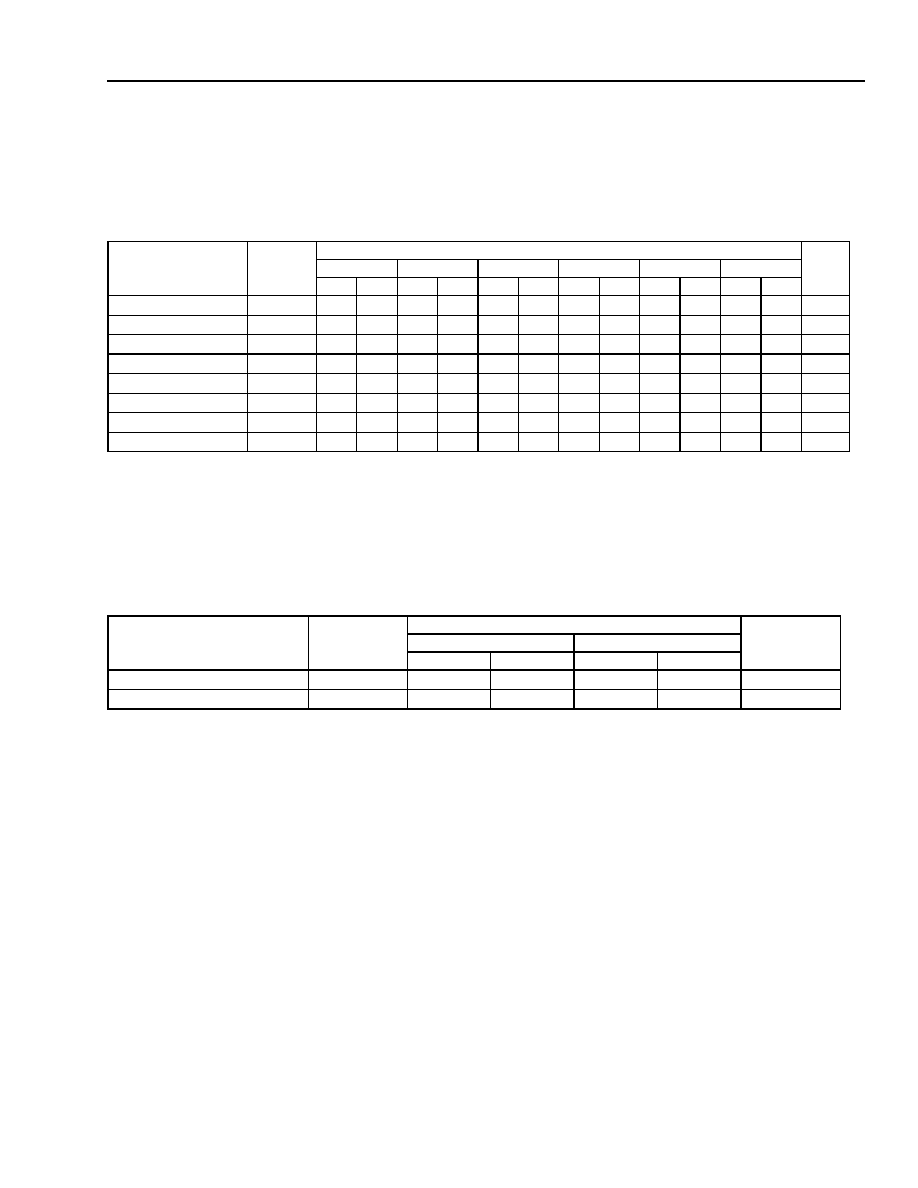
Data Sheet
June 1999
ORCA Series 2 FPGAs
Lucent Technologies Inc.
149
Timing Characteristics
(continued)
Notes:
This clock delay is for a fully routed clock tree that uses the primary clock network. It includes both the input buffer delay and the clock routing
to the PFU CLK input. The delay will be reduced if any of the clock branches are not used.
Speed grades of -5, -6, and -7 are for OR2TxxA devices only.
Note: This clock delay is for a fully routed clock tree that uses the primary clock network. It includes both the input buffer delay and the clock
routing to the PFU CLK input. The delay will be reduced if any of the clock branches are not used.
Table 42A. OR2CxxA and OR2TxxA Internal Clock Delay
OR2CxxA Commercial: V
DD
= 5.0 V ± 5%, 0 ∞C
T
A
70 ∞C; OR2CxxA Industrial: V
DD
= 5.0 V ± 10%, ≠40 ∞C
T
A
+85 ∞C.
OR2TxxA Commercial: V
DD
= 3.0 V to 3.6 V, 0 ∞C
T
A
70 ∞C; OR2TxxA Industrial: V
DD
= 3.0 V to 3.6 V, ≠40 ∞C
T
A
+85 ∞C.
Device
(T
J
= 85 ∞C, V
DD
= min)
Symbol
Speed
Unit
-2
-3
-4
-5
-6
-7
Min
Max
Min
Max
Min
Max
Min
Max
Min
Max
Min
Max
OR2C04A/OR2T04A
CLK_DEL
--
4.6
--
4.4
--
4.3
--
3.6
--
--
--
--
ns
OR2C06A/OR2T06A CLK_DEL
--
4.7
--
4.5
--
4.4
--
3.7
--
--
--
--
ns
OR2C08A/OR2T08A CLK_DEL
--
4.8
--
4.6
--
4.5
--
3.8
--
--
--
--
ns
OR2C10A/OR2T10A CLK_DEL
--
4.9
--
4.7
--
4.6
--
3.9
--
--
--
--
ns
OR2C12A/OR2T12A CLK_DEL
--
5.0
--
4.8
--
4.7
--
4.0
--
--
--
--
ns
OR2C15A/OR2T15A
CLK_DEL
--
5.1
--
4.9
--
4.8
--
4.1
--
3.9
--
3.3
ns
OR2C26A/OR2T26A
CLK_DEL
--
5.2
--
5.1
--
5.0
--
4.2
--
4.0
--
3.4
ns
OR2C40A/OR2T40A
CLK_DEL
--
5.6
--
5.4
--
5.3
--
4.5
--
4.2
--
3.6
ns
Table 42B. OR2TxxB Internal Clock Delay
OR2TxxB Commercial: V
DD
= 3.0 V to 3.6 V, 0 ∞C
T
A
70 ∞C; OR2TxxB Industrial: V
DD
= 3.0 V to 3.6 V, ≠40 ∞C
T
A
+85
∞C.
Device
(T
J
= 85 ∞C, V
DD
= min)
Symbol
Speed
Unit
-7
-8
Min
Max
Min
Max
OR2T15B
CLK_DEL
--
3.6
--
3.1
ns
OR2T40B
CLK_DEL
--
3.8
--
3.3
ns

Data Sheet
ORCA Series 2 FPGAs
June 1999
150
Lucent Technologies Inc.
Timing Characteristics
(continued)
Notes:
The pin-to-pin timing information from
ORCA
Foundry version 9.2 and later is more accurate than this table. For earlier versions of
ORCA
Foundry, the pin-to-pin timing parameters in this table should be used instead of results reported by
ORCA
Foundry.
This clock delay is for a fully routed clock tree that uses the primary clock network. It includes both the input buffer delay, the clock routing to
the PFU CLK input, the clock
Q of the FF, and the delay through the output buffer. The delay will be reduced if any of the clock branches are
not used. The given timing requires that the input clock pin be located at one of the four center PICs on any side of the device and that the
direct FF
I/O routing be used.
If the clock pin is not located at one of the four center PICs, this delay must be increased by up to the following amounts:
OR2C/2T04A = 1.5%, OR2C/2T06A = 2.0%, OR2C/2T08A = 3.1%, OR2C/2T10A = 3.9%, OR2C/2T12A = 4.9%, OR2C/2T15A = 5.7%,
OR2C/2T26A = 8.1%, OR2C/2T40A = 12.5%.
Speed grades of -5, -6, and -7 are for OR2TxxA devices only.
Table 43A. OR2CxxA and OR2TxxA OR2CxxA/OR2TxxA Global Clock to Output Delay (Pin-to-Pin)--Output
on Same Side of the Device as the Clock Pin
OR2CxxA Commercial: V
DD
= 5.0 V ± 5%, 0 ∞C
T
A
70 ∞C; Industrial: V
DD
= 5.0 V ± 10%, ≠40 ∞C
T
A
+85 ∞C; C
L
= 50 pF.
OR2TxxA Commercial: V
DD
= 3.0 V to 3.6 V, 0 ∞C
T
A
70 ∞C; Industrial:
V
DD
= 3.0 V to 3.6 V,
≠40
∞C
T
A
+85 ∞C;
C
L
=
50 pF.
Description
(T
J
= 85 ∞C, V
DD
= min)
Device
Speed
Unit
-2
-3
-4
-5
-6
-7
Min
Max
Min
Max
Min
Max
Min
Max
Min
Max
Min
Max
CLK Input Pin
OUTPUT Pin
(Fast)
OR2C/2T04A
OR2C/2T06A
OR2C/2T08A
OR2C/2T10A
OR2C/2T12A
OR2C/2T15A
OR2C/2T26A
OR2C/2T40A
--
--
--
--
--
--
--
--
11.7
11.8
11.9
12.0
12.1
12.2
12.3
12.7
--
--
--
--
--
--
--
--
10.3
10.4
10.5
10.6
10.7
10.8
11.0
11.4
--
--
--
--
--
--
--
--
9.8
9.9
10.0
10.1
10.2
10.3
10.5
10.8
--
--
--
--
--
--
--
--
8.6
8.7
8.8
8.9
9.0
9.1
9.2
9.5
--
--
--
--
--
--
--
--
--
--
--
--
--
8.3
8.4
8.6
--
--
--
--
--
--
--
--
--
--
--
--
--
6.7
6.9
7.0
ns
ns
ns
ns
ns
ns
ns
ns
CLK Input Pin
OUTPUT Pin
(Slewlim)
OR2C/2T04A
OR2C/2T06A
OR2C/2T08A
OR2C/2T10A
OR2C/2T12A
OR2C/2T15A
OR2C/2T26A
OR2C/2T40A
--
--
--
--
--
--
--
--
13.9
14.0
14.1
14.2
14.3
14.4
14.5
14.9
--
--
--
--
--
--
--
--
12.5
12.6
12.7
12.8
12.9
13.0
13.2
13.6
--
--
--
--
--
--
--
--
11.7
11.8
11.9
12.0
12.1
12.2
12.3
12.6
--
--
--
--
--
--
--
--
10.0
10.1
10.2
10.3
10.4
10.5
10.6
10.9
--
--
--
--
--
--
--
--
--
--
--
--
--
9.5
9.6
9.8
--
--
--
--
--
--
--
--
--
--
--
--
--
7.4
7.5
7.7
ns
ns
ns
ns
ns
ns
ns
ns
CLK Input Pin
OUTPUT Pin
(Sinklim)
OR2C/2T04A
OR2C/2T06A
OR2C/2T08A
OR2C/2T10A
OR2C/2T12A
OR2C/2T15A
OR2C/2T26A
OR2C/2T40A
--
--
--
--
--
--
--
--
15.7
15.8
15.9
16.0
16.1
16.2
16.3
16.7
--
--
--
--
--
--
--
--
14.7
14.8
14.9
15.0
15.1
15.2
15.3
15.7
--
--
--
--
--
--
--
--
13.7
13.8
13.9
14.0
14.1
14.2
14.3
14.6
--
--
--
--
--
--
--
--
13.1
13.2
13.3
13.4
13.5
13.6
13.7
14.0
--
--
--
--
--
--
--
--
--
--
--
--
--
12.1
12.2
12.4
--
--
--
--
--
--
--
--
--
--
--
--
--
10.0
10.7
10.9
ns
ns
ns
ns
ns
ns
ns
ns

Data Sheet
June 1999
ORCA Series 2 FPGAs
Lucent Technologies Inc.
151
Timing Characteristics
(continued)
Notes:
The pin-to-pin timing information from
ORCA
Foundry version 9.2 and later is more accurate than this table. For earlier versions of
ORCA
Foundry,
the pin-to-pin timing parameters in this table should be used instead of results reported by
ORCA
Foundry.
This clock delay is for a fully routed clock tree that uses the primary clock network. It includes both the input buffer delay, the clock routing to the
PFU CLK input, the clock
Q of the FF, and the delay through the output buffer. The delay will be reduced if any of the clock branches are not
used. The given timing requires that the input clock pin be located at one of the four center PICs on any side of the device and that the direct
FF
I/O routing be used.
If the clock pin is not located at one of the four center PICs, this delay must be increased by up to the following amounts:
OR2T15B = 5.7%, OR2T40B = 12.5%.
Figure 62. Global Clock to Output Delay
Table 43B. OR2TxxB Global Clock to Output Delay (Pin-to-Pin)--Output on Same Side of the Device as the
Clock Pin
OR2TxxB Commercial: V
DD
= 3.0 V to 3.6 V, 0 ∞C
T
A
70 ∞C;
Industrial: V
DD
= 3.0 V to 3.6 V, ≠40 ∞C
T
A
+85 ∞C; C
L
= 50 pF.
Description
(T
J
= 85 ∞C, V
DD
= min)
Device
Speed
Unit
-7
-8
Min
Max
Min
Max
CLK Input Pin
OUTPUT Pin
(Fast)
OR2T15B
OR2T40B
--
--
7.3
7.5
--
--
6.6
6.6
ns
ns
CLK Input Pin
OUTPUT Pin
(Slewlim)
OR2T15B
OR2T40B
--
--
8.2
8.4
--
--
7.4
7.6
ns
ns
CLK Input Pin
OUTPUT Pin
(Sinklim)
OR2T15B
OR2T40B
--
--
12.9
13.1
--
--
12.1
12.3
ns
ns
5-4846(F)
OUTPUT (50 pF LOAD)
Q
D
CLK

Data Sheet
ORCA Series 2 FPGAs
June 1999
152
Lucent Technologies Inc.
Timing Characteristics
(continued)
Notes:
The pin-to-pin timing information from
ORCA
Foundry version 9.2 and later is more accurate than this table. For earlier versions of
ORCA
Foundry, the pin-to-pin timing parameters in this table should be used instead of results reported by
ORCA
Foundry.
This clock delay is for a fully routed clock tree that uses the primary clock network. It includes both the input buffer delay, the clock routing to the
PFU CLK input, the clock
Q of the FF, and the delay through the output buffer. The delay will be reduced if any of the clock branches are not
used. The given timing requires that the input clock pin be located at one of the four center PICs on any side of the device and that the direct
FF
I/O routing be used.
If the clock pin is not located at one of the four center PICs, this delay must be increased by up to the following amounts:
OR2C/2T04A = 1.5%, OR2C/2T06A = 2.0%, OR2C/2T08A = 3.1%, OR2C/2T10A = 3.9%, OR2C/2T12A = 4.9%, OR2C/2T15A = 5.7%,
OR2C/2T26A = 8.1%, OR2C/2T40A = 12.5%.
Speed grades of -5, -6, and -7 are for OR2TxxA devices only
Table 44A. OR2CxxA/OR2TxxA Global Clock to Output Delay (Pin-to-Pin)--Output Not on Same
Side of the Device as the Clock Pin
OR2CxxA Commercial: V
DD
= 5.0 V ± 5%, 0 ∞C
T
A
70 ∞C; Industrial: V
DD
= 5.0 V ± 10%, ≠40 ∞C
T
A
+85 ∞C; C
L
= 50 pF.
OR2TxxA Commercial: V
DD
= 3.0 V to 3.6 V, 0 ∞C
T
A
70 ∞C;
Industrial: V
DD
= 3.0 V to 3.6 V, ≠40 ∞C
T
A
+85 ∞C; C
L
= 50 pF.
Description
(T
J
= 85 ∞C, V
DD
= min)
Device
Speed
Unit
-2
-3
-4
-5
-6
-7
Min
Max
Min
Max
Min
Max
Min
Max
Min
Max
Min
Max
CLK Input Pin
OUTPUT Pin
(Fast)
OR2C/2T04A
OR2C/2T06A
OR2C/2T08A
OR2C/2T10A
OR2C/2T12A
OR2C/2T15A
OR2C/2T26A
OR2C/2T40A
--
--
--
--
--
--
--
--
11.8
12.0
12.2
12.4
12.6
12.8
13.1
14.4
--
--
--
--
--
--
--
--
10.5
10.6
10.8
11.0
11.2
11.5
11.9
13.3
--
--
--
--
--
--
--
--
9.9
10.0
10.1
10.3
10.5
10.7
11.1
12.4
--
--
--
--
--
--
--
--
8.8
8.9
9.0
9.2
9.4
9.6
10.0
11.1
--
--
--
--
--
--
--
--
--
--
--
--
--
8.9
9.3
10.5
--
--
--
--
--
--
--
--
--
--
--
--
--
7.3
7.7
8.3
ns
ns
ns
ns
ns
ns
ns
ns
CLK Input Pin
OUTPUT Pin
(Slewlim)
OR2C/2T04A
OR2C/2T06A
OR2C/2T08A
OR2C/2T10A
OR2C/2T12A
OR2C/2T15A
OR2C/2T26A
OR2C/2T40A
--
--
--
--
--
--
--
--
14.1
14.3
14.4
14.6
14.8
15.0
15.3
16.7
--
--
--
--
--
--
--
--
12.7
12.9
13.1
13.3
13.5
13.6
14.1
15.5
--
--
--
--
--
--
--
--
11.8
11.9
12.0
12.2
12.4
12.6
12.9
14.2
--
--
--
--
--
--
--
--
10.3
10.4
10.5
10.6
10.8
11.0
11.4
12.5
--
--
--
--
--
--
--
--
--
--
--
--
--
10.1
10.5
11.7
--
--
--
--
--
--
--
--
--
--
--
--
--
8.0
8.4
9.1
ns
ns
ns
ns
ns
ns
ns
ns
CLK Input Pin
OUTPUT Pin
(Sinklim)
OR2C/2T04A
OR2C/2T06A
OR2C/2T08A
OR2C/2T10A
OR2C/2T12A
OR2C/2T15A
OR2C/2T26A
OR2C/2T40A
--
--
--
--
--
--
--
--
15.9
16.0
16.2
16.4
16.6
16.8
17.1
18.5
--
--
--
--
--
--
--
--
14.8
15.0
15.2
15.4
15.6
15.8
16.2
17.6
--
--
--
--
--
--
--
--
13.8
13.9
14.1
14.2
14.4
14.6
14.9
16.3
--
--
--
--
--
--
--
--
13.4
13.5
13.6
13.7
13.9
14.1
14.4
15.6
--
--
--
--
--
--
--
--
--
--
--
--
--
12.7
13.1
14.3
--
--
--
--
--
--
--
--
--
--
--
--
--
11.2
11.6
12.2
ns
ns
ns
ns
ns
ns
ns
ns

Data Sheet
June 1999
ORCA Series 2 FPGAs
Lucent Technologies Inc.
153
.
Timing Characteristics
(continued)
Notes:
The pin-to-pin timing information from
ORCA
Foundry version 9.2 and later is more accurate than this table. For earlier versions of
ORCA
Foundry,
the pin-to-pin timing parameters in this table should be used instead of results reported by
ORCA
Foundry.
This clock delay is for a fully routed clock tree that uses the primary clock network. It includes both the input buffer delay, the clock routing to the
PFU CLK input, the clock
Q of the FF, and the delay through the output buffer. The delay will be reduced if any of the clock branches are not
used. The given timing requires that the input clock pin be located at one of the four center PICs on any side of the device and that the direct
FF
I/O routing be used.
If the clock pin is not located at one of the four center PICs, this delay must be increased by up to the following amounts:
OR2T15B = 5.7%, OR2T40B = 12.5%.
Figure 63. Global Clock to Output Delay
Table 44B. OR2TxxB Global Clock to Output Delay (Pin-to-Pin)--Output Not on Same Side of the Device as
the Clock Pin
OR2TxxB Commercial: V
DD
= 3.0 V to 3.6 V, 0 ∞C
T
A
70 ∞C;
Industrial: V
DD
= 3.0 V to 3.6 V, ≠40 ∞C
T
A
+85 ∞C; C
L
= 50 pF.
Description
(T
J
= 85 ∞C, V
DD
= min)
Device
Speed
Unit
-7
-8
Min
Max
Min
Max
CLK Input Pin
OUTPUT Pin
(Fast)
OR2T15B
OR2T40B
--
--
7.6
8.1
--
--
6.9
7.4
ns
ns
CLK Input Pin
OUTPUT Pin
(Slewlim)
OR2T15B
OR2T40B
--
--
8.4
9.0
--
--
7.7
8.2
ns
ns
CLK Input Pin
OUTPUT Pin
(Sinklim)
OR2T15B
OR2T40B
--
--
13.2
13.7
--
--
12.4
12.8
ns
ns
OUTPUT (50 pF LOAD)
Q
D
CLK
5-4846(F)

Data Sheet
ORCA Series 2 FPGAs
June 1999
154
Lucent Technologies Inc.
Timing Characteristics
(continued)
Notes:
The pin-to-pin timing parameters in this table should be used instead of results reported by
ORCA
Foundry.
This clock delay is for a fully routed clock tree that uses the primary clock network. It includes both the input buffer delay and the clock routing to
the PFU CLK input. The delay will be reduced if any of the clock branches are not used. The given Setup (Delayed and No delay) and Hold
(Delayed) timing allows the input clock pin to be located in any PIC on any side of the device, but direct I/O
FF routing must be used. The Hold
(No delay) timing assumes the clock pin is located at one of the four center PICs and direct I/O
FF routing is used. If it is not located at one of
the four center PICs, this delay must be increased by up to the following amounts: OR2C/2T04A = 5.3%, OR2C/2T06A = 6.4%, OR2C/2T08A =
7.3%, OR2C/2T10A = 9.1%, OR2C/2T12A = 10.8%, OR2C/2T15A = 12.2%, OR2C/2T26A = 16.1%, OR2C/2T40A = 21.2%.
Speed grades of -5, -6, and -7 are for OR2TxxA devices only.
Table 45A. OR2CxxA/OR2TxxA Global Input to Clock Setup/Hold Time (Pin-to-Pin)
OR2CxxA Commercial: V
DD
= 5.0 V ± 5%, 0 ∞C
T
A
70 ∞C; Industrial: V
DD
= 5.0 V ± 10%, ≠40 ∞C
T
A
+85 ∞C.
OR2TxxA Commercial: V
DD
= 3.0 V to 3.6 V, 0 ∞C
T
A
70 ∞C; Industrial: V
DD
= 3.0 V to 3.6 V, ≠40 ∞C
T
A
+85 ∞C.
Description
(T
J
= all, V
DD
= all)
Device
Speed
Unit
-2
-3
-4
-5
-6
-7
Min
Max
Min
Max
Min
Max
Min
Max
Min
Max
Min
Max
Input to CLK (TTL/CMOS)
Setup Time (no delay)
OR2C/2T04A
OR2C/2T06A
OR2C/2T08A
OR2C/2T10A
OR2C/2T12A
OR2C/2T15A
OR2C/2T26A
OR2C/2T40A
0.0
0.0
0.0
0.0
0.0
0.0
0.0
0.0
--
--
--
--
--
--
--
--
0.0
0.0
0.0
0.0
0.0
0.0
0.0
0.0
--
--
--
--
--
--
--
--
0.0
0.0
0.0
0.0
0.0
0.0
0.0
0.0
--
--
--
--
--
--
--
--
0.0
0.0
0.0
0.0
0.0
0.0
0.0
0.0
--
--
--
--
--
--
--
--
--
--
--
--
--
0.0
0.0
0.0
--
--
--
--
--
--
--
--
--
--
--
--
--
0.0
0.0
0.0
--
--
--
--
--
--
--
--
ns
ns
ns
ns
ns
ns
ns
ns
Input to CLK (TTL/CMOS)
Setup Time (delayed)
OR2C/2T04A
OR2C/2T06A
OR2C/2T08A
OR2C/2T10A
OR2C/2T12A
OR2C/2T15A
OR2C/2T26A
OR2C/2T40A
5.8
5.7
5.6
5.3
5.2
4.9
7.3
6.8
--
--
--
--
--
--
--
--
5.5
5.4
5.3
5.0
4.9
4.7
6.9
6.4
--
--
--
--
--
--
--
--
4.2
4.1
4.0
3.9
3.8
3.6
6.0
5.5
--
--
--
--
--
--
--
--
4.0
3.9
3.8
3.7
3.6
3.4
5.7
5.2
--
--
--
--
--
--
--
--
--
--
--
--
--
4.1
6.7
6.5
--
--
--
--
--
--
--
--
--
--
--
--
--
4.1
6.0
5.8
--
--
--
--
--
--
--
--
ns
ns
ns
ns
ns
ns
ns
ns
Input to CLK (TTL/CMOS)
Hold Time (no delay)
OR2C/2T04A
OR2C/2T06A
OR2C/2T08A
OR2C/2T10A
OR2C/2T12A
OR2C/2T15A
OR2C/2T26A
OR2C/2T40A
4.2
4.3
4.5
4.8
5.0
5.4
6.2
7.9
--
--
--
--
--
--
--
--
4.0
4.1
4.3
4.6
4.8
5.1
5.8
6.8
--
--
--
--
--
--
--
--
3.8
3.9
4.1
4.4
4.6
4.9
5.6
6.6
--
--
--
--
--
--
--
--
3.6
3.7
3.9
4.2
4.4
4.7
5.3
6.3
--
--
--
--
--
--
--
--
--
--
--
--
--
4.2
4.6
5.8
--
--
--
--
--
--
--
--
--
--
--
--
--
3.7
4.1
4.9
--
--
--
--
--
--
--
--
ns
ns
ns
ns
ns
ns
ns
ns
Input to CLK (TTL/CMOS)
Hold Time (delayed)
OR2C/2T04A
OR2C/2T06A
OR2C/2T08A
OR2C/2T10A
OR2C/2T12A
OR2C/2T15A
OR2C/2T26A
OR2C/2T40A
0.0
0.0
0.0
0.0
0.0
0.0
0.0
0.0
--
--
--
--
--
--
--
--
0.0
0.0
0.0
0.0
0.0
0.0
0.0
0.0
--
--
--
--
--
--
--
--
0.0
0.0
0.0
0.0
0.0
0.0
0.0
0.0
--
--
--
--
--
--
--
--
0.0
0.0
0.0
0.0
0.0
0.0
0.0
0.0
--
--
--
--
--
--
--
--
--
--
--
--
--
0.0
0.0
0.0
--
--
--
--
--
--
--
--
--
--
--
--
--
0.0
0.0
0.0
--
--
--
--
--
--
--
--
ns
ns
ns
ns
ns
ns
ns
ns
Data Sheet
June 1999
ORCA Series 2 FPGAs
Lucent Technologies Inc.
155
Timing Characteristics
(continued)
Notes:
The pin-to-pin timing parameters in this table should be used instead of results reported by
ORCA
Foundry.
This clock delay is for a fully routed clock tree that uses the primary clock network. It includes both the input buffer delay and the clock routing to
the PFU CLK input. The delay will be reduced if any of the clock branches are not used. The given Setup (delayed and no delay) and Hold
(delayed) timing allows the input clock pin to be located in any PIC on any side of the device, but direct I/O
FF routing must be used. The Hold
(no delay) timing assumes the clock pin is located at one of the four center PICs and direct I/O
FF routing is used. If it is not located at one of
the four center PICs, this delay must be increased by up to the following amounts: OR2T15B = 5.7%, OR2T40B = 12.5%.
Figure 64. Global Input to Clock Setup/Hold Time
Table 45B. OR2TxxB Global Input to Clock Setup/Hold Time (Pin-to-Pin)
OR2TxxB Commercial: V
DD
= 3.0 V to 3.6 V, 0 ∞C
T
A
70 ∞C; Industrial: V
DD
= 3.0 V to 3.6 V, ≠40 ∞C
T
A
+85 ∞C.
Description
(T
J
= all, V
DD
= all)
Device
Speed
Unit
-7
-8
Min
Max
Min
Max
Input to CLK (TTL/CMOS)
Setup Time (no delay)
OR2T15B
OR2T40B
0.0
0.0
--
--
0.0
0.0
--
--
ns
ns
Input to CLK (TTL/CMOS)
Setup Time (delayed)
OR2T15B
OR2T40B
4.7
7.7
--
--
4.0
5.5
--
--
ns
ns
Input to CLK (TTL/CMOS)
Hold Time (no delay)
OR2T15B
OR2T40B
1.6
1.4
--
--
1.4
1.3
--
--
ns
ns
Input to CLK (TTL/CMOS)
Hold Time (delayed)
OR2T15B
OR2T40B
0.0
0.0
--
--
0.0
0.0
--
--
ns
ns
Q
D
CLK
INPUT
5-4847(F)

Data Sheet
ORCA Series 2 FPGAs
June 1999
156
Lucent Technologies Inc.
Timing Characteristics
(continued)
Notes:
If the input buffer is placed in delay mode, the chip hold time to the nearest PFU latch is guaranteed to be 0 if the clock is routed using the
primary clock network; (T
J
= all, V
DD
= all). It should also be noted that any signals routed on the clock lines or using the TRIDI buffers directly
from the input buffer do not get delayed at any time.
The delays for all input buffers assume an input rise/fall time of
1 V/ns.
Speed grades of -5, -6, and -7 are for OR2TxxA devices only
Table 46A. OR2CxxA/OR2TxxA Programmable I/O Cell Timing Characteristics
OR2CxxA Commercial: V
DD
= 5.0 V ± 5%, 0 ∞C
T
A
70 ∞C; OR2CxxA Industrial: V
DD
= 5.0 V ± 10%, ≠40 ∞C
T
A
+85 ∞C.
OR2TxxA Commercial: V
DD
= 3.0 V to 3.6 V, 0 ∞C
T
A
70 ∞C; OR2TxxA Industrial: V
DD
= 3.0 V to 3.6 V, ≠40 ∞C
T
A
+85
∞C.
Parameter
Symbol
Speed
Unit
-2
-3
-4
-5
-6
-7
Min
Max
Min
Max
Min
Max
Min
Max
Min
Max
Min
Max
Inputs (T
J
= 85 ∞C, V
DD
= min)
Input Rise Time
T
R
--
500
--
500
--
500
--
500
--
500
--
500
ns
Input Fall Time
T
F
--
500
--
500
--
500
--
500
--
500
--
500
ns
Pad to In Delay
PAD_IN_DEL
--
1.7
--
1.5
--
1.3
--
1.2
--
1.2
--
1.1
ns
Pad to Nearest PFU Latch Output
CHIP_LATCH
--
6.2
--
4.7
--
4.1
--
3.5
--
3.1
--
2.9
ns
Delay Added to General Routing
(input buffer in delay mode for
OR2C/2T15A and smaller
devices)
--
--
8.1
--
7.0
--
6.0
--
5.9
--
6.2
--
5.8
ns
Delay Added to General Routing
(input buffer in delay mode for
OR2C/2T26A and OR2C/2T40A)
--
--
11.0
--
9.7
--
8.6
--
8.6
--
9.0
--
8.6
ns
Delay Added to Direct-FF Routing
(input buffer in delay mode for
OR2C/2T15A and smaller
devices)
--
--
8.0
--
6.8
--
5.9
--
6.0
--
6.4
--
6.0
ns
Delay Added to Direct-FF Routing
(input buffer in delay mode for
OR2C/2T26A and OR2C/2T40A)
--
--
10.9
--
10.2
--
8.5
--
8.6
--
9.1
--
7.9
ns
Outputs (T
J
= 85 ∞C, V
DD
= min, C
L
= 50 pF)
PFU CK to Pad Delay (DOUT[3:0] to
PAD):
Fast
Slewlim
Sinklim
DOUT_DEL(F)
DOUT_DEL(SL)
DOUT_DEL(SI)
--
--
--
7.1
9.4
11.2
--
--
--
6.2
8.4
10.5
--
--
--
5.5
7.4
9.4
--
--
--
5.0
6.4
9.5
--
--
--
4.4
5.6
8.3
--
--
--
3.3
4.1
7.2
ns
ns
ns
Output to Pad Delay (OUT[3:0] to
PAD):
Fast
Slewlim
Sinklim
OUT_DEL(F)
OUT_DEL(SL)
OUT_DEL(SI)
--
--
--
5.0
6.7
9.8
--
--
--
4.0
6.3
7.2
--
--
--
3.6
5.5
7.5
--
--
--
3.1
4.5
7.6
--
--
--
2.7
3.9
6.5
--
--
--
2.3
3.1
6.2
ns
ns
ns
3-state Enable Delay (TS[3:0] to
PAD):
Fast
Slewlim
Sinklim
TS_DEL(F)
TS_DEL(SL)
TS_DEL(SI)
--
--
--
5.8
7.5
10.6
--
--
--
4.7
7.0
7.9
--
--
--
4.0
6.3
8.4
--
--
--
3.5
5.2
9.3
--
--
--
3.1
4.7
8.0
--
--
--
2.5
3.7
7.6
ns
ns
ns

Data Sheet
June 1999
ORCA Series 2 FPGAs
Lucent Technologies Inc.
157
.
Timing Characteristics
(continued)
Notes:
If the input buffer is placed in delay mode, the chip hold time to the nearest PFU latch is guaranteed to be 0 if the clock is routed using the
primary clock network; (T
J
= all, V
DD
= all). It should also be noted that any signals routed on the clock lines or using the TRIDI buffers directly
from the input buffer do not get delayed at any time.
The delays for all input buffers assume an input rise/fall time of
1 V/ns.
Table 46B. OR2TxxB Programmable I/O Cell Timing Characteristics
OR2TxxA Commercial: V
DD
= 3.0 V to 3.6 V, 0 ∞C
T
A
70 ∞C; OR2TxxA Industrial: V
DD
= 3.0 V to 3.6 V, ≠40 ∞C
T
A
+85
∞C.
Parameter
Symbol
Speed
Unit
-7
-8
Min
Max
Min
Max
Inputs (T
J
= 85 ∞C, V
DD
= min)
Input Rise Time
T
R
--
500
--
500
ns
Input Fall Time
T
F
--
500
--
500
ns
Pad to In Delay
PAD_IN_DEL
--
1.1
--
1.0
ns
Pad to Nearest PFU Latch Output
CHIP_LATCH
--
3.3
--
2.4
ns
Delay Added to General Routing
(input buffer in delay mode for
OR2T15B and smaller devices)
--
--
6.6
--
6.1
ns
Delay Added to General Routing
(input buffer in delay mode for
OR2T40B)
--
--
8.9
--
8.2
ns
Delay Added to Direct-FF Routing
(input buffer in delay mode for
OR2T15B and smaller devices)
--
--
6.4
--
6.0
ns
Delay Added to Direct-FF Routing
(input buffer in delay mode for
OR2T40B)
--
--
8.7
--
8.0
ns
Outputs (T
J
= 85 ∞C, V
DD
= min, C
L
= 50 pF)
PFU CK to Pad Delay (DOUT[3:0] to
PAD):
Fast
Slewlim
Sinklim
DOUT_DEL(F)
DOUT_DEL(SL)
DOUT_DEL(SI)
--
--
--
2.8
3.6
8.3
--
--
--
2.5
3.3
8.0
ns
ns
ns
Output to Pad Delay (OUT[3:0] to
PAD):
Fast
Slewlim
Sinklim
OUT_DEL(F)
OUT_DEL(SL)
OUT_DEL(SI)
--
--
--
2.8
3.6
8.3
--
--
--
2.5
3.3
8.0
ns
ns
ns
3-state Enable Delay (TS[3:0] to
PAD):
Fast
Slewlim
Sinklim
TS_DEL(F)
TS_DEL(SL)
TS_DEL(SI)
--
--
--
3.0
3.8
9.1
--
--
--
2.7
3.4
8.7
ns
ns
ns
Data Sheet
ORCA Series 2 FPGAs
June 1999
158
Lucent Technologies Inc.
Timing Characteristics
(continued)
Table 47. Series 2 General Configuration Mode Timing Characteristics
OR2CxxA Commercial: V
DD
= 5.0 V ± 5%, 0 ∞C
T
A
70 ∞C; OR2CxxA Industrial: V
DD
= 5.0 V ± 10%, ≠40 ∞C
T
A
+85 ∞C.
OR2TxxA/B Commercial: V
DD
= 3.0 V to 3.6 V, 0 ∞C
T
A
70 ∞C; OR2TxxA/B Industrial: V
DD
= 3.0 V to 3.6 V,
≠40 ∞C
T
A
+85
∞C.
Parameter
Symbol
Min
Max
Unit
All Configuration Modes
M[3:0] Setup Time to
INIT
High
T
SMODE
50.0
--
ns
M[3:0] Hold Time from
INIT
High
T
HMODE
600.0
--
ns
RESET
Pulse Width Low to Start Reconfiguration
T
RW
50.0
--
ns
PRGM
Pulse Width Low to Start Reconfiguration
T
PGW
50.0
--
ns
Master and Asynchronous Peripheral Modes
Power-on Reset Delay
CCLK Period (M3 = 0)
(M3 = 1)
Configuration Latency (noncompressed):
OR2C/2T04A (M3
=
0)
(M3 = 1)
OR2C/2T06A (M3
=
0)
(M3 = 1)
OR2C/2T08A (M3
=
0)
(M3 = 1)
OR2C/2T10A (M3
=
0)
(M3 = 1)
OR2C/2T12A (M3
=
0)
(M3 = 1)
OR2C/2T15A/2T15B (M3 = 0)
(M3 = 1)
OR2C/2T26A (M3
=
0)
(M3 = 1)
OR2C/2T40A/2T40B (M3 = 0)
(M3 = 1)
T
PO
T
CCLK
T
CL
17.30
66.0
528.00
4.31
34.48
6.00
48.00
7.62
60.96
9.82
78.56
11.86
94.88
14.57
116.56
20.25
162.00
31.29
250.32
69.47
265.00
2120.00
17.30*
138.40*
24.08*
192.64*
30.60*
244.80*
39.43*
315.44*
47.62*
380.96*
58.51*
468.08*
81.32*
650.56*
125.62*
1004.96*
ms
ns
ns
ms
ms
ms
ms
ms
ms
ms
ms
ms
ms
ms
ms
ms
ms
ms
ms
Slave Serial and Synchronous Peripheral Modes
Power-on Reset Delay
CCLK Period (OR2CxxA/OR2TxxA)
CCLK Period (OR2TxxB)
Configuration Latency (noncompressed):
OR2C/2T04A
OR2C/2T06A
OR2C/2T08A
OR2C/2T10A
OR2C/2T12A
OR2C/2T15A
OR2T15B
OR2C/2T26A
OR2C/2T40A
OR2T40B
T
PO
T
CCLK
T
CCLK
T
CL
4.33
100.00
25.00
6.53
9.09
11.55
14.88
17.97
22.08
5.52
30.69
47.40
11.85
17.37
--
--
--
--
--
--
--
--
--
--
--
--
ms
ns
ns
ms
ms
ms
ms
ms
ms
ms
ms
ms
ms
* Not applicable to asynchronous peripheral mode.

Data Sheet
June 1999
ORCA Series 2 FPGAs
Lucent Technologies Inc.
159
Note: T
PO
is triggered when V
DD
reaches between 3.0 V to 4.0 V for the OR2CxxA and between 2.7 V and 3.0 V for the OR2TxxA/OR2TxxB.
Slave Parallel Mode
Power-on Reset Delay
CCLK Period (OR2CxxA/OR2TxxA)
CCLK Period (OR2TxxB)
Configuration Latency (noncompressed):
OR2C/2T04A
OR2C/2T06A
OR2C/2T08A
OR2C/2T10A
OR2C/2T12A
OR2C/2T15A
OR2T15B
OR2C/2T26A
OR2C/2T40A
OR2T40B
T
PO
T
CCLK
T
CCLK
T
CL
4.33
100.00
25.0
0.82
1.14
1.44
1.86
2.25
2.76
0.69
3.84
5.93
1.48
17.37
--
--
--
--
--
--
--
--
--
--
--
--
ms
ns
ns
ms
ms
ms
ms
ms
ms
ms
ms
ms
ms
Partial Reconfiguration (noncompressed):
OR2C/2T04A
OR2C/2T06A
OR2C/2T08A
OR2C/2T10A
OR2C/2T12A
OR2C/2T15A/2T15B
OR2C/2T26A
OR2C/2T40A/2T40B
T
PR
1.70
2.00
2.20
2.50
2.70
3.00
3.50
4.30
--
--
--
--
--
--
--
--
µs/frame
µs/frame
µs/frame
µs/frame
µs/frame
µs/frame
µs/frame
µs/frame
INIT
Timing
INIT
High to CCLK Delay:
Slave Parallel
Slave Serial
Synchronous Peripheral
Master Serial:
(M3 = 1)
(M3 = 0)
Master Parallel:
(M3 = 1)
(M3 = 0)
T
INIT_CLK
1.00
1.00
1.00
1.06
0.59
5.28
1.12
--
--
--
4.51
2.65
21.47
4.77
µs
µs
µs
µs
µs
µs
µs
Initialization Latency (
PRGM
high to
INIT
high):
OR2C/2T04A
OR2C/2T06A
OR2C/2T08A
OR2C/2T10A
OR2C/2T12A
OR2C/2T15A/2T15B
OR2C/2T26A
OR2C/2T40A/2T40B
T
IL
63.36
74.98
86.59
98.21
109.82
121.44
144.67
181.90
254.40
301.04
347.68
394.32
440.96
487.60
580.88
730.34
µs
µs
µs
µs
µs
µs
µs
µs
INIT
High to
WR
, Asynchronous Peripheral
T
INIT_WR
1.50
--
µs
Timing Characteristics
(continued)
Table 47. Series 2 General Configuration Mode Timing Characteristics (continued)
OR2CxxA Commercial: V
DD
= 5.0 V ± 5%, 0 ∞C
T
A
70 ∞C; OR2CxxA Industrial: V
DD
= 5.0 V ± 10%, ≠40 ∞C
T
A
+85 ∞C.
OR2TxxA/B Commercial: V
DD
= 3.0 V to 3.6 V, 0 ∞C
T
A
70 ∞C; OR2TxxA/B Industrial: V
DD
= 3.0 V to 3.6 V,
≠40 ∞C
T
A
+85
∞C.
Parameter
Symbol
Min
Max
Unit

Data Sheet
ORCA Series 2 FPGAs
June 1999
160
Lucent Technologies Inc.
Timing Characteristics
(continued)
Series 2
Figure 65. General Configuration Mode Timing Diagram
5-4531(F)
V
DD
CCLK
M[3:0]
PRGM
INIT
T
PO
+ T
IL
T
IL
T
CCLK
T
SMODE
T
HMODE
T
INIT_CLK
DONE
T
CL
T
PGW

Data Sheet
June 1999
ORCA Series 2 FPGAs
Lucent Technologies Inc.
161
Timing Characteristics
(continued)
Note: Serial configuration data is transmitted out on DOUT on the falling edge of CCLK after it is input DIN.
Figure 66. Master Serial Configuration Mode Timing Diagram
Table 48. Series 2 Master Serial Configuration Mode Timing Characteristics
OR2CxxA Commercial: V
DD
= 5.0 V ± 5%, 0 ∞C
T
A
70 ∞C; OR2CxxA Industrial: V
DD
= 5.0 V ± 10%, ≠40 ∞C
T
A
+85 ∞C.
OR2TxxA/B Commercial: V
DD
= 3.0 V to 3.6 V, 0 ∞C
T
A
70 ∞C; OR2TxxA/B Industrial: V
DD
= 3.0 V to 3.6 V,
≠40 ∞C
T
A
+85
∞C.
Parameter
Symbol
Min
Nom
Max
Unit
DIN Setup Time
T
S
60.0
--
--
ns
DIN Hold Time
T
H
0
--
--
ns
CCLK Frequency (M3 = 0)
F
C
3.8
10.0
15.2
MHz
CCLK Frequency (M3 = 1)
F
C
0.48
1.25
1.9
MHz
CCLK to DOUT Delay
T
D
--
--
30
ns
5-4532(F)
DIN
CCLK
DOUT
T
S
T
H
BIT N
T
D
BIT N
Data Sheet
ORCA Series 2 FPGAs
June 1999
162
Lucent Technologies Inc.
Timing Characteristics
(continued)
Notes:
The RCLK period consists of seven CCLKs for RCLK low and one CCLK for RCLK high.
Serial data is transmitted out on DOUT 1.5 CCLK cycles after the byte is input D[7:0]
f.44(F)
Figure 67. Master Parallel Configuration Mode Timing Diagram
Table 49. Series 2 Master Parallel Configuration Mode Timing Characteristics
OR2CxxA Commercial: V
DD
= 5.0 V ± 5%, 0 ∞C
T
A
70 ∞C; OR2CxxA Industrial: V
DD
= 5.0 V ± 10%, ≠40 ∞C
T
A
+85 ∞C.
OR2TxxA/B Commercial: V
DD
= 3.0 V to 3.6 V, 0 ∞C
T
A
70 ∞C; OR2TxxA/B Industrial: V
DD
= 3.0 V to 3.6 V,
≠40 ∞C
T
A
+85
∞C.
Parameter
Symbol
Min
Max
Unit
RCLK to Address Valid
T
AV
0
200
ns
D[7:0] Setup Time to RCLK High
T
S
60
--
ns
D[7:0] Hold Time to RCLK High
T
H
0
--
ns
RCLK Low Time (M3 = 0)
T
CL
462
1855
ns
RCLK High Time (M3 = 0)
T
CH
66
265
ns
RCLK Low Time (M3 = 1)
T
CL
3696
14840
ns
RCLK High Time (M3 = 1)
T
CH
528
2120
ns
CCLK to DOUT
T
D
--
30
ns
A[17:0]
RCLK
D[7:0]
T
CL
T
CH
T
AV
CCLK
DOUT
T
H
T
S
BYTE N
BYTE N + 1
D0
D1
D2
D3
D4
D5
D6
D7
T
D

Data Sheet
June 1999
ORCA Series 2 FPGAs
Lucent Technologies Inc.
163
Timing Characteristics
(continued)
* This parameter is valid whether the end of not RDY is determined from the RDY/RCLK pin or from the D7 pin.
Notes:
Serial data is transmitted out on DOUT on the falling edge of CCLK after the byte is input D[7:0].
D[6:0] timing is the same as the write data port of the D7 waveform because D[6:0] are not enabled.
Figure 68. Asynchronous Peripheral Configuration Mode Timing Diagram
Table 50. Series 2 Asynchronous Peripheral Configuration Mode Timing Characteristics
OR2CxxA Commercial: V
DD
= 5.0 V ± 5%, 0 ∞C
T
A
70 ∞C; OR2CxxA Industrial: V
DD
= 5.0 V ± 10%, ≠40 ∞C
T
A
+85 ∞C.
OR2TxxA/B Commercial: V
DD
= 3.0 V to 3.6 V, 0 ∞C
T
A
70 ∞C; OR2TxxA/B Industrial: V
DD
= 3.0 V to 3.6 V,
≠40 ∞C
T
A
+85
∞C.
Parameter
Symbol
Min
Max
Unit
WR
,
CS0
, and CS1 Pulse Width
T
WR
100
--
ns
D[7:0] Setup Time
T
S
20
--
ns
D[7:0] Hold Time
T
H
0
--
ns
RDY Delay
T
RDY
--
60
ns
RDY Low
T
B
1
8
CCLK Periods
Earliest
WR
After RDY Goes High*
T
WR2
0
--
ns
RD
to D7 Enable/Disable
T
DEN
--
60
ns
CCLK to DOUT
T
D
--
30
ns
5-4533.a
CS1
D7
CCLK
DOUT
CS0
RDY
D0
D1
D2
T
B
T
WR
T
S
T
H
T
RDY
WR
D7
T
D
PREVIOUS BYTE
T
WR2
WRITE DATA
D3
T
DEN
T
DEN
RD

Data Sheet
ORCA Series 2 FPGAs
June 1999
164
Lucent Technologies Inc.
Timing Characteristics
(continued)
Note: Serial data is transmitted out on DOUT 1.5 clock cycles after the byte is input D[7:0].
Note: Serial data is transmitted out on DOUT 1.5 clock cycles after the byte is input D[7:0].
Figure 69. Synchronous Peripheral Configuration Mode Timing Diagram
Table 51A. OR2CxxA/OR2TxxA Synchronous Peripheral Configuration Mode Timing Characteristics
OR2CxxA Commercial: V
DD
= 5.0 V ± 5%, 0 ∞C
T
A
70 ∞C; OR2CxxA Industrial: V
DD
= 5.0 V ± 10%, ≠40 ∞C
T
A
+85 ∞C.
OR2TxxA Commercial: V
DD
= 3.0 V to 3.6 V, 0 ∞C
T
A
70 ∞C; OR2TxxA Industrial: V
DD
= 3.0 V to 3.6 V, ≠40 ∞C
T
A
+85
∞C.
Parameter
Symbol
Min
Max
Unit
D[7:0] Setup Time
T
S
20
--
ns
D[7:0] Hold Time
T
H
0
--
ns
CCLK High Time
T
CH
50
--
ns
CCLK Low Time
T
CL
50
--
ns
CCLK Frequency
F
C
--
10
MHz
CCLK to DOUT
T
D
--
30
ns
Table 51B. OR2TxxB Synchronous Peripheral Configuration Mode Timing Characteristics
OR2TxxB Commercial: V
DD
= 3.0 V to 3.6 V, 0 ∞C
T
A
70 ∞C; OR2TxxB Industrial: V
DD
= 3.0 V to 3.6 V, ≠40 ∞C
T
A
+85
∞C.
Parameter
Symbol
Min
Max
Unit
D[7:0] Setup Time
T
S
15
--
ns
D[7:0] Hold Time
T
H
0
--
ns
CCLK High Time
T
CH
12.5
--
ns
CCLK Low Time
T
CL
12.5
--
ns
CCLK Frequency
F
C
--
40
MHz
CCLK to DOUT
T
D
--
10
ns
5-4534(F)
CCLK
INIT
D[7:0]
DOUT
RDY
0
1
2
3
4
BYTE 0
BYTE 1
T
INIT_CLK
T
CH
T
CL
T
H
T
S
T
D
5
6
7
0

Data Sheet
June 1999
ORCA Series 2 FPGAs
Lucent Technologies Inc.
165
Timing Characteristics
(continued)
Note: Serial configuration data is transmitted out on DOUT on the falling edge of CCLK after it is input on DIN.
Note: Serial configuration data is transmitted out on DOUT on the falling edge of CCLK after it is input on DIN
Figure 70. Slave Serial Configuration Mode Timing Diagram
Table 52A. OR2CxxA/OR2TxxA Slave Serial Configuration Mode Timing Characteristics
OR2CxxA Commercial: V
DD
= 5.0 V ± 5%, 0 ∞C
T
A
70 ∞C; OR2CxxA Industrial: V
DD
= 5.0 V ± 10%, ≠40 ∞C
T
A
+85 ∞C.
OR2TxxA Commercial: V
DD
= 3.0 V to 3.6 V, 0 ∞C
T
A
70 ∞C; OR2TxxA Industrial: V
DD
= 3.0 V to 3.6 V, ≠40 ∞C
T
A
+85
∞C
Parameter
Symbol
Min
Max
Unit
DIN Setup Time
T
S
20
--
ns
DIN Hold Time
T
H
0
--
ns
CCLK High Time
T
CH
50
--
ns
CCLK Low Time
T
CL
50
--
ns
CCLK Frequency
F
C
--
10
MHz
CCLK to DOUT
T
D
--
30
ns
Table 52B. OR2TxxB Slave Serial Configuration Mode Timing Characteristics
OR2TxxB Commercial: V
DD
= 3.0 V to 3.6 V, 0 ∞C
T
A
70 ∞C; OR2TxxB Industrial: V
DD
= 3.0 V to 3.6 V, ≠40 ∞C
T
A
+85
∞C.
Parameter
Symbol
Min
Max
Unit
DIN Setup Time
T
S
15
--
ns
DIN Hold Time
T
H
0
--
ns
CCLK High Time
T
CH
12.5
--
ns
CCLK Low Time
T
CL
12.5
--
ns
CCLK Frequency
F
C
--
40
MHz
CCLK to DOUT
T
D
--
10
ns
5-4535(F)
DIN
CCLK
DOUT
T
D
T
S
T
H
T
CL
T
CH
BIT N
BIT N

Data Sheet
ORCA Series 2 FPGAs
June 1999
166
Lucent Technologies Inc.
Timing Characteristics
(continued)
Note: Daisy chaining of FPGAs is not supported in this mode.
Note: Daisy chaining of FPGAs is not supported in this mode.
Figure 71. Slave Parallel Configuration Mode Timing Diagram
Table 53A. OR2CxxA/OR2TxxA Slave Parallel Configuration Mode Timing Characteristics
OR2CxxA Commercial: V
DD
= 5.0 V ± 5%, 0 ∞C
T
A
70 ∞C; OR2CxxA Industrial: V
DD
= 5.0 V ± 10%, ≠40 ∞C
T
A
+85 ∞C.
OR2TxxA Commercial: V
DD
= 3.0 V to 3.6 V, 0 ∞C
T
A
70 ∞C; OR2TxxA Industrial: V
DD
= 3.0 V to 3.6 V, ≠40 ∞C
T
A
+85
∞C.
Parameter
Symbol
Min
Max
Unit
CS0
, CS1,
WR
Setup Time
T
S1
60
--
ns
CS0
, CS1,
WR
Hold Time
T
H1
20
--
ns
D[7:0] Setup Time
T
S2
20
--
ns
D[7:0] Hold Time
T
H2
0
--
ns
CCLK High Time
T
CH
50
--
ns
CCLK Low Time
T
CL
50
--
ns
CCLK Frequency
F
C
--
10
MHz
Table 53B. OR2TxxB Slave Parallel Configuration Mode Timing Characteristics
OR2TxxB Commercial: V
DD
= 3.0 V to 3.6 V, 0 ∞C
T
A
70 ∞C; OR2TxxB Industrial: V
DD
= 3.0 V to 3.6 V, ≠40 ∞C
T
A
+85
∞C.
Parameter
Symbol
Min
Max
Unit
CS0
, CS1,
WR
Setup Time
T
S1
--
--
--
CS0
, CS1,
WR
Hold Time
T
H1
15
--
ns
D[7:0] Setup Time
T
S2
15
--
ns
D[7:0] Hold Time
T
H2
0
--
ns
CCLK High Time
T
CH
12.5
--
ns
CCLK Low Time
T
CL
12.5
--
ns
CCLK Frequency
F
C
--
40
MHz
5-2848(F)
T
S1
T
H1
T
S2
T
H2
CS1
CCLK
D[7:0]
CS0
WR

Data Sheet
June 1999
ORCA Series 2 FPGAs
Lucent Technologies Inc.
167
Timing Characteristics
(continued)
Figure 72. Readback Timing Diagram
Table 54. Series 2 Readback Timing Characteristics
OR2CxxA Commercial: V
DD
= 5.0 V ± 5%, 0 ∞C
T
A
70 ∞C; OR2CxxA Industrial: V
DD
= 5.0 V ± 10%, ≠40 ∞C
T
A
+85 ∞C.
OR2TxxA/B Commercial: V
DD
= 3.0 V to 3.6 V, 0 ∞C
T
A
70 ∞C; OR2TxxA/B Industrial: V
DD
= 3.0 V to 3.6 V,
≠40 ∞C
T
A
+85
∞C.
Parameter
Symbol
Min
Max
Unit
RD_CFGN
to CCLK Setup Time
T
S
50
--
ns
RD_CFGN
High Width to Abort Readback
T
RBA
2
--
CCLK
CCLK Low Time
T
CL
50
--
ns
CCLK High Time
T
CH
50
--
ns
CCLK Frequency
F
C
--
10
MHz
CCLK to RD_DATA Delay
T
D
--
50
ns
5-4536(F)
T
D
T
CH
CCLK
RD_DATA
T
S
T
CL
RD_CFGN
BIT 0
BIT 1
BIT 0
T
RBA

Data Sheet
ORCA Series 2 FPGAs
June 1999
168
Lucent Technologies Inc.
Timing Characteristics
(continued)
BSTD(F).2c.r3
Figure 73. Boundary-Scan Timing Diagram
Table 55. Series 2 Boundary-Scan Timing Characteristics
OR2CxxA Commercial: V
DD
= 5.0 V ± 5%, 0 ∞C
T
A
70 ∞C; OR2CxxA Industrial: V
DD
= 5.0 V ± 10%, ≠40 ∞C
T
A
+85 ∞C.
OR2TxxA Commercial: V
DD
= 3.0 V to 3.6 V, 0 ∞C
T
A
70 ∞C; OR2TxxA Industrial: V
DD
= 3.0 V to 3.6 V, ≠40 ∞C
T
A
+85
∞C.
OR2TxxB Commercial: V
DD
= 3.0 V to 3.6 V, 0 ∞C
T
A
70 ∞C; OR2TxxB Industrial: V
DD
= 3.0 V to 3.6 V, ≠40 ∞C
T
A
+85
∞C.
Parameter
Symbol
Min
Max
Unit
TDI/TMS to TCK Setup Time
T
S
25
--
ns
TDI/TMS Hold Time from TCK
T
H
0
--
ns
TCK Low Time
T
CL
50
--
ns
TCK High Time
T
CH
50
--
ns
TCK to TDO Delay
T
D
--
20
ns
TCK Frequency
T
TCK
--
10
MHz
TCK
TMS
TDI
TDO
T
S
T
H
T
D

Data Sheet
June 1999
ORCA Series 2 FPGAs
Lucent Technologies Inc.
169
Measurement Conditions
5-3234(F).r1
Figure 74. ac Test Loads
5-3233(F).ar4
Figure 75. Output Buffer Delays
5-3235(F).a
Figure 76. Input Buffer Delays
50 pF
A. Load Used to Measure Propagation Delay
TO THE OUTPUT UNDER TEST
TO THE OUTPUT UNDER TEST
50 pF
V
CC
GND
1 k
B. Load Used to Measure Rising/Falling Edges
V
DD
T
PHH
V
DD
/2
V
SS
OUT[I]
PAD
OUT
1.5 V
0.0 V
T
PLL
PAD
OUT[I]
ac TEST LOADS (SHOWN ABOVE)
TS[I]
OUT
0.0 V
1.5 V
T
PHH
T
PLL
PAD
IN[I]
IN
3.0 V
V
SS
V
DD
/2
V
DD
PAD IN
IN[I]

Lucent Technologies Inc.
170
Data Sheet
June 1999
ORCA Series 2 FPGAs
Output Buffer Characteristics
OR2CxxA
5-4634(F)
Figure 77. Sinklim (T
J
= 25 ∞C, V
DD
= 5.0 V)
5-4636(F)
Figure 78. Slewlim (T
J
= 25 ∞C, V
DD
= 5.0 V)
5-4638(F)
Figure 79. Fast (T
J
= 25 ∞C, V
DD
= 5.0 V)
5-4635(F)
Figure 80. Sinklim (T
J
= 125 ∞C, V
DD
= 4.5 V)
5-4637(F)
Figure 81. Slewlim (T
J
= 125 ∞C, V
DD
= 4.5 V)
5-4639(F)
Figure 82. Fast (T
J
= 125 ∞C, V
DD
= 4.5 V)
70
60
50
40
30
20
10
0
OUTPUT CURREN
T
, I
O
(mA
)
0
1
2
3
4
5
OUTPUT VOLTAGE, V
O
(V)
I
OL
I
OH
250
225
150
100
50
0
OUTPUT CURRENT
, I
O
(m
A
)
0
1
2
3
4
OUTPUT VOLTAGE, V
O
(V)
I
OL
I
OH
5
200
175
125
75
25
250
225
150
100
50
0
OUTP
UT C
URRENT
,
I
O
(m
A
)
0
1
2
3
4
OUTPUT VOLTAGE, V
O
(V)
I
OL
I
OH
5
200
175
125
75
25
50
40
30
20
10
0
OUTPUT CURRENT
,
I
O
(m
A
)
0
1
2
3
4
OUTPUT VOLTAGE, V
O
(V)
I
OL
I
OH
5
150
125
100
75
50
0
OUTPUT
CURR
ENT
,
I
O
(mA
)
0
1
2
3
4
OUTPUT VOLTAGE, V
O
(V)
I
OL
I
OH
25
175
125
100
75
50
0
OUTPUT CURRENT
,
I
O
(m
A
)
0
1
2
3
4
OUTPUT VOLTAGE, V
O
(V)
I
OL
I
OH
25
150

171
Lucent Technologies Inc.
Data Sheet
ORCA Series 2 FPGAs
June 1999
Output Buffer Characteristics
(continued)
OR2TxxA
5-4637(F)
Figure 83. Sinklim (T
J
= 25 ∞C, V
DD
= 3.3 V)
5-4637(F)
Figure 84. Slewlim (T
J
= 25 ∞C, V
DD
= 3.3 V)
5-4637(F)
Figure 85. Fast (T
J
= 25 ∞C, V
DD
= 3.3 V)
5-4637(F)
Figure 86. Sinklim (T
J
= 125 ∞C, V
DD
= 3.0 V)
5-4637(F)
Figure 87. Slewlim (T
J
= 125 ∞C, V
DD
= 3.0 V)
5-4637(F)
Figure 88. Fast (T
J
= 125 ∞C, V
DD
= 3.0 V)
0.0 0.5
1.0
1.5
2.0
2.5
3.0 3.5
0
20
40
60
80
OUTPUT VOLTAGE, V
O
(V)
I
OL
70
50
30
10
I
OH
OUTP
UT CUR
RENT
,
I
O
(mA
)
0.0 0.5
1.0
1.5
2.0
2.5
3.0 3.5
0
60
100
120
140
OUTPUT VOLTAGE, V
O
(V)
OUTP
UT CUR
RENT
,
I
O
(mA
)
I
OL
I
OH
80
40
20
0.0 0.5
1.0
1.5
2.0
2.5
3.0 3.5
0
60
100
120
140
OUTPUT VOLTAGE, V
O
(V)
OUTP
UT CUR
RENT
,
I
O
(mA
)
I
OL
I
OH
80
40
20
0.0
0.5
1.0
1.5
2.0
2.5
3.0
0
5
10
30
40
OUTPUT VOLTAGE, V
O
(V)
OUTP
UT CU
RRENT,
I
O
(
m
A
)
I
OL
I
OH
25
20
15
35
0.0
0.5
1.0
1.5
2.0
2.5
3.0
0
10
20
70
OUTPUT VOLTAGE, V
O
(V)
OUTP
UT C
URRENT, I
O
(mA
)
I
OL
I
OH
50
40
30
60
0.0
0.5
1.0
1.5
2.0
2.5
3.0
0
10
20
70
OUTPUT VOLTAGE, V
O
(V)
OUTPUT CURRENT
,
I
O
(m
A
)
I
OL
I
OH
50
40
30
60

Lucent Technologies Inc.
172
Data Sheet
June 1999
ORCA Series 2 FPGAs
Output Buffer Characteristics
(continued)
OR2TxxB
5-7927(F).r1
Figure 89. Sinklim (T
J
= 25 ∞C, V
DD
= 3.3 V)
5-7928(F).r1
Figure 90. Slewlim (T
J
= 25 ∞C, V
DD
= 3.3 V)
5-7929(F).r1
Figure 91. Fast (T
J
= 25 ∞C, V
DD
= 3.3 V)
5-7930(F).r1
Figure 92. Sinklim (T
J
= 125 ∞C, V
DD
= 3.0 V)
5-7931(F).r1
Figure 93. Slewlim (T
J
= 125 ∞C, V
DD
= 3.0 V)
5-7932(F).r1
Figure 94. Fast (T
J
= 125 ∞C, V
DD
= 3.0 V)
0.0 0.5 1.0 1.5 2.0 2.5 3.0 3.5
90
80
I
OL
60
50
40
30
20
10
0
OUTPUT VOLTAGE, V
O
(V)
OUTPUT CURRE
NT
,
I
O
(m
A)
I
OH
0.0 0.5 1.0 1.5 2.0 2.5 3.0 3.5
180
160
140
120
100
80
60
40
20
0
OUTPUT VOLTAGE, V
O
(V)
OUT
P
UT CUR
RENT,
I
O
(m
A)
I
OL
I
OH
0.0 0.5 1.0 1.5 2.0 2.5 3.0 3.5
180
160
140
120
100
80
60
40
20
0
OUTPUT VOLTAGE, V
O
(V)
OUTPUT C
URRENT,
I
O
(m
A)
I
OL
I
OH
0.0
0.5
1.0
1.5
2.0
2.5
3.0
55
50
40
30
25
20
15
10
05
0
OUTPUT VOLTAGE, V
O
(V)
OUTPUT C
URRENT,
I
O
(m
A)
45
35
I
OL
I
OH
0.0
0.5
1.0
1.5
2.0
2.5
3.0
110
100
80
60
50
40
30
20
10
0
OUTPUT VOLTAGE, V
O
(V)
OUTPUT C
URRENT,
I
O
(m
A)
90
70
I
OL
I
OH
0.0
0.5
1.0
1.5
2.0
2.5
3.0
110
100
80
60
50
40
30
20
10
0
OUTPUT VOLTAGE, V
O
(V)
OUTP
UT
CURRE
NT,
I
O
(mA
)
90
70
I
OL
I
OH

Data Sheet
June 1999
ORCA Series 2 FPGAs
Lucent Technologies Inc.
173
Package Outline Drawings
Terms and Definitions
Basic Size (BSC):
The basic size of a dimension is the size from which the limits for that dimension are derived
by the application of the allowance and the tolerance.
Design Size:
The design size of a dimension is the actual size of the design, including an allowance for fit
and tolerance.
Minimum (MIN) or
Maximum (MAX):
Indicates the minimum or maximum allowable size of a dimension.
Reference (REF):
The reference dimension is an untoleranced dimension used for informational purposes only.
It is a repeated dimension or one that can be derived from other values in the drawing.
Typical (TYP):
When specified after a dimension, this indicates the repeated design size if a tolerance is
specified or repeated basic size if a tolerance is not specified.

Data Sheet
ORCA Series 2 FPGAs
June 1999
174
Lucent Technologies Inc.
Package Outline Drawings
(continued)
84-Pin PLCC
Dimensions are in millimeters.
5-2347r.16
1.27 TYP
0.330/0.533
0.10
SEATING PLANE
0.51 MIN
TYP
5.080
MAX
PIN #1 IDENTIFIER ZONE
11
75
53
33
12
32
54
74
29.083
±
0.076
30.353 MAX
30.353
MAX
1
29.083
±
0.076
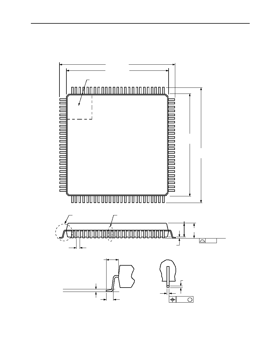
Data Sheet
June 1999
ORCA Series 2 FPGAs
Lucent Technologies Inc.
175
Package Outline Drawings
(continued)
100-Pin TQFP
Dimensions are in millimeters.
5-2146r.15
0.50 TYP
1.60 MAX
SEATING PLANE
0.08
1.40
±
0.05
0.05/0.15
DETAIL A
DETAIL B
14.00
±
0.20
16.00
±
0.20
76
100
1
25
26
50
51
75
14.00
±
0.20
16.00
±
0.20
PIN #1 IDENTIFIER ZONE
DETAIL B
0.19/0.27
0.08
M
0.106/0.200
DETAIL A
0.45/0.75
GAGE PLANE
SEATING PLANE
1.00 REF
0.25

Data Sheet
ORCA Series 2 FPGAs
June 1999
176
Lucent Technologies Inc.
Package Outline Drawings
(continued)
144-Pin TQFP
Dimensions are in millimeters.
5-3815r.5
DETAIL B
0.19/0.27
0.08
M
0.106/0.200
DETAIL A
0.45/0.75
GAGE PLANE
SEATING PLANE
1.00 REF
0.25
1.60 MAX
SEATING PLANE
0.08
0.50 TYP
1.40
±
0.05
0.05/0.15
DETAIL A
DETAIL B
PIN #1 IDENTIFIER ZONE
20.00
±
0.20
22.00
±
0.20
109
144
1
36
37
72
73
108
20.00
±
0.20
22.00
±
0.20

Data Sheet
June 1999
ORCA Series 2 FPGAs
Lucent Technologies Inc.
177
Package Outline Drawings
(continued)
160-Pin QFP
Dimensions are in millimeters.
5-2132r.12
81
120
28.00
± 0.20
31.20
± 0.20
DETAIL A
DETAIL B
4.07 MAX
0.65 TYP
SEATING PLANE
0.10
3.42 ± 0.25
0.25 MIN
1
40
121
160
PIN #1 IDENTIFIER ZONE
31.20 ± 0.20
28.00 ± 0.20
80
41
0.22/0.38
0.12
M
0.13/0.23
DETAIL B
0.25
0.73/1.03
1.60 REF
GAGE PLANE
SEATING PLANE
DETAIL A

Data Sheet
ORCA Series 2 FPGAs
June 1999
178
Lucent Technologies Inc.
Package Outline Drawings
(continued)
208-Pin SQFP
Dimensions are in millimeters.
5-2196r.13
156
105
30.60 ± 0.20
157
208
1
52
53
104
28.00 ± 0.20
28.00
± 0.20
30.60
± 0.20
PIN #1 IDENTIFIER ZONE
4.10 MAX
0.08
3.40 ± 0.20
SEATING PLANE
0.25 MIN
0.50 TYP
DETAIL B
DETAIL A
0.50/0.75
GAGE PLANE
SEATING PLANE
1.30 REF
0.25
DETAIL A
DETAIL B
0.17/0.27
0.10
M
0.090/0.200

Data Sheet
June 1999
ORCA Series 2 FPGAs
Lucent Technologies Inc.
179
Package Outline Drawings
(continued)
208-Pin SQFP2
Dimensions are in millimeters.
5-3828.a
156
105
30.60
±
0.20
157
208
1
52
53
104
28.00
±
0.20
EXPOSED HEAT SINK APPEARS ON BOTTOM
SURFACE: CHIP BONDED FACE UP (SEE DETAIL C)
28.00
±
0.20
30.60
±
0.20
PIN #1 IDENTIFIER ZONE
21.0
REF
21.0 REF
4.10 MAX
0.08
3.40
±
0.20
SEATING PLANE
0.25 MIN
0.50 TYP
DETAIL B
DETAIL A
0.50/0.75
GAGE PLANE
SEATING PLANE
1.30 REF
0.25
DETAIL A
DETAIL B
0.17/0.2
0.10
M
0.090/0.200
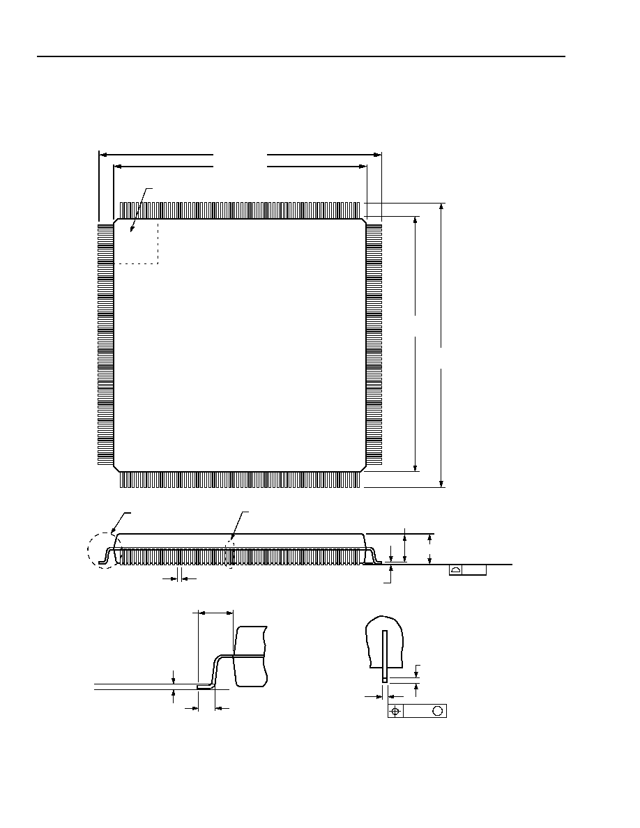
Data Sheet
ORCA Series 2 FPGAs
June 1999
180
Lucent Technologies Inc.
Package Outline Drawings
(continued)
240-Pin SQFP
Dimensions are in millimeters.
5-2718r.8
0.08
3.40 ± 0.20
SEATING PLANE
0.25 MIN
0.50 TYP
DETAIL A
DETAIL B
180
121
181
240
34.60 ± 0.20
1
32.00 ± 0.20
60
61
120
PIN #1 IDENTIFIER ZONE
32.00
± 0.20
0.50/0.75
GAGE PLANE
SEATING PLANE
1.30 REF
0.25
DETAIL A
DETAIL B
0.17/0.27
0.10
M
0.090/0.200
4.10 MAX
34.60
± 0.20
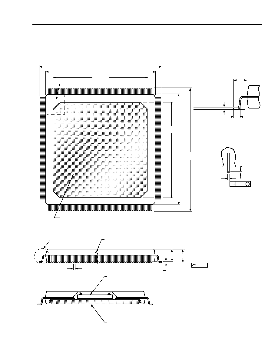
Data Sheet
June 1999
ORCA Series 2 FPGAs
Lucent Technologies Inc.
181
Package Outline Drawings
(continued)
240-Pin SQFP2
Dimensions are in millimeters.
5-3825r.8
0.50/0.75
GAGE PLANE
SEATING PLANE
1.30 REF
0.25
DETAIL A
DETAIL B
0.17/0.27
0.10
M
0.090/0.200
CHIP
CHIP BONDED FACE UP
COPPER HEAT SINK
0.08
3.40
±
0.20
SEATING PLANE
0.25 MIN
0.50 TYP
DETAIL A
DETAIL B
180
121
181
240
34.60
±
0.20
1
32.00
±
0.20
60
61
120
PIN #1 IDENTI FIER ZONE
32.00
±
0.20
34.60
±
0.20
EXPOSED HEAT SINK APPEARS ON
TOP SURFACE IN CHIP FACE-DOWN VERSION OR
BOTTOM SURFACE IN CHIP FACE-UP VERSION
24.2
REF
24. 2 REF
4.10 MAX

Data Sheet
ORCA Series 2 FPGAs
June 1999
182
Lucent Technologies Inc.
Package Outline Drawings
(continued)
256-Pin PBGA
Dimensions are in millimeters.
5-4406r.6
0.36
±
0.04
1.17
±
0.05
2.13
±
0.19
SEATING PLANE
SOLDER BALL
0.60
±
0.10
0.20
PWB
MOLD
COMPOUND
27.00
±
0.20
27.00
±
0.20
24.00
+0.70
≠0.00
24.00
+0.70
≠0.00
A1 BALL
IDENTIFIER ZONE
A
B
C
D
E
F
G
H
J
K
L
M
Y
N
P
R
T
U
V
W
1 2 3 4 5 6 7 8 9 10
11
12
13
14
15
16
17
18
20
19
CENTER ARRAY
FOR THERMAL
ENHANCEMENT
19 SPACES @ 1.27 = 24.13
A1 BALL
CORNER
19 SPACES
@ 1.27 = 24.13
0.75
±
0.15
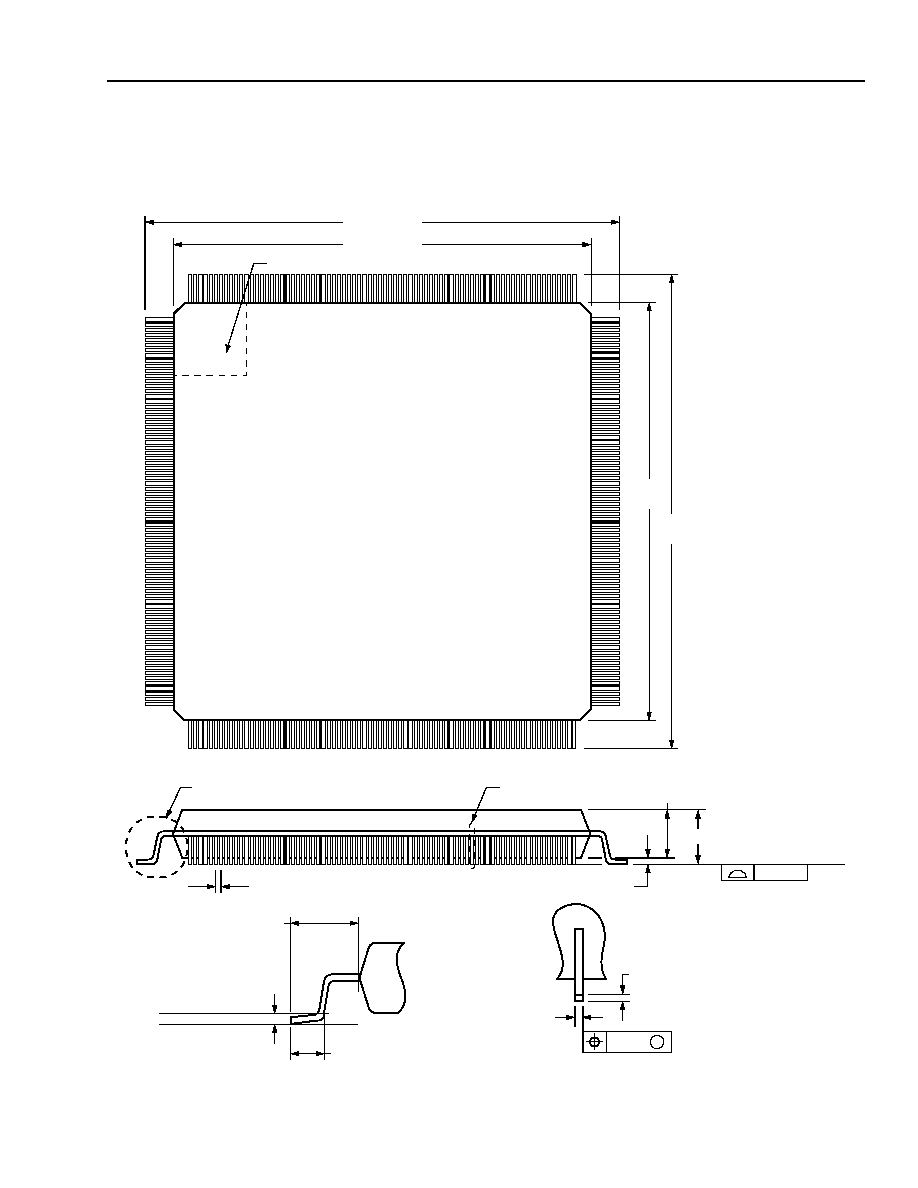
Data Sheet
June 1999
ORCA Series 2 FPGAs
Lucent Technologies Inc.
183
Package Outline Drawings
(continued)
304-Pin SQFP
Dimensions are in millimeters.
5-3307r.8
DETAIL A
DETAIL B
4.10 MAX
0.50 TYP
SEATING PLANE
0.08
3.40 ± 0.20
0.25 MIN
0.17/0.27
0.10
M
0.090/0.200
DETAIL B
0.25
0.50/0.75
1.30 REF
GAGE PLANE
SEATING PLANE
DETAIL A
PIN #1 IDENTIFIER ZONE
42.60 ± 0.20
40.00 ± 0.20
42.60
± 0.20
40.00
± 0.20
1
76
77
152
153
228
229
304
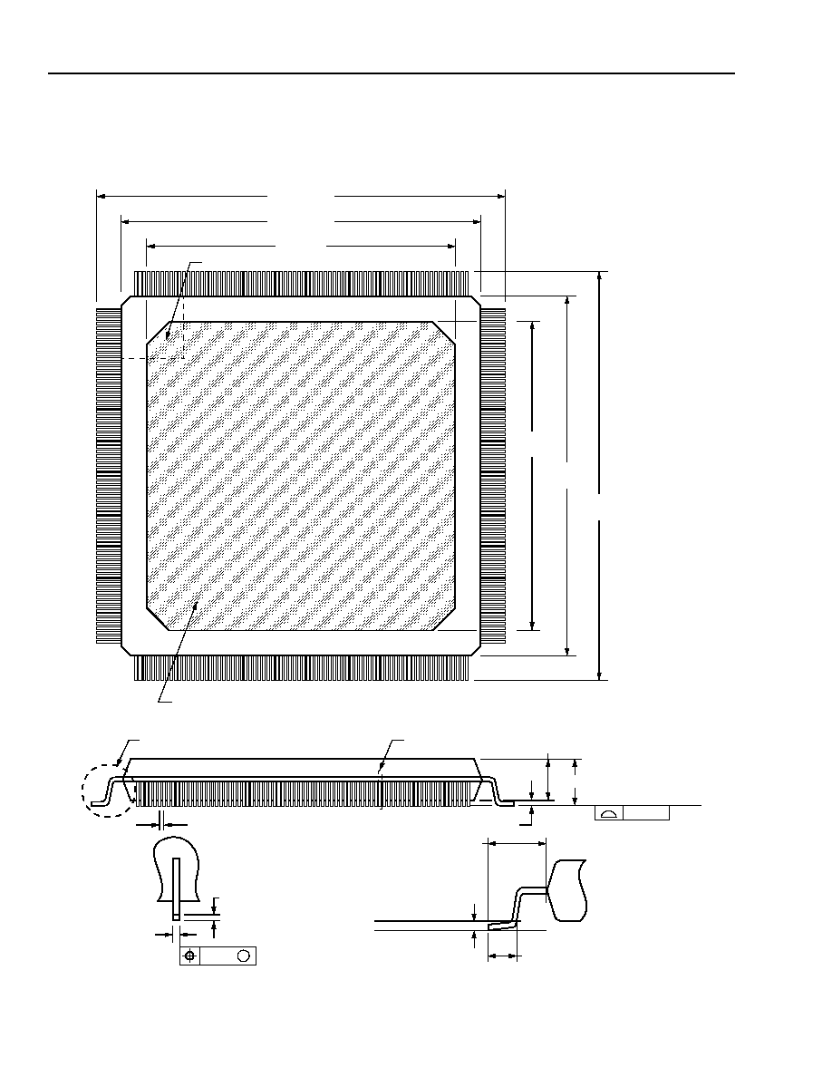
Data Sheet
ORCA Series 2 FPGAs
June 1999
184
Lucent Technologies Inc.
Package Outline Drawings
(continued)
304-Pin SQFP2
Dimensions are in millimeters.
5-3827(F).r8
DETAIL A
DETAIL B
4.10 MAX
0.50 TYP
SEATING PLANE
0.08
3.40 ± 0.20
0.25 MIN
0.17/0.27
0.10
M
0.090/0.200
DETAIL B
0.25
0.50/0.75
1.30 REF
GAGE PLANE
SEATING PLANE
DETAIL A
42.60 ± 0.20
40.00 ± 0.20
42.60
± 0.20
40.00
± 0.20
1
76
77
152
153
228
229
304
PIN #1 IDENTIFIER ZONE
EXPOSED HEAT SINK APPEARS ON
TOP SURFACE IN CHIP FACE-DOWN VERSION OR
BOTTOM SURFACE IN CHIP FACE-UP VERSION
31.2 REF
31.2
REF
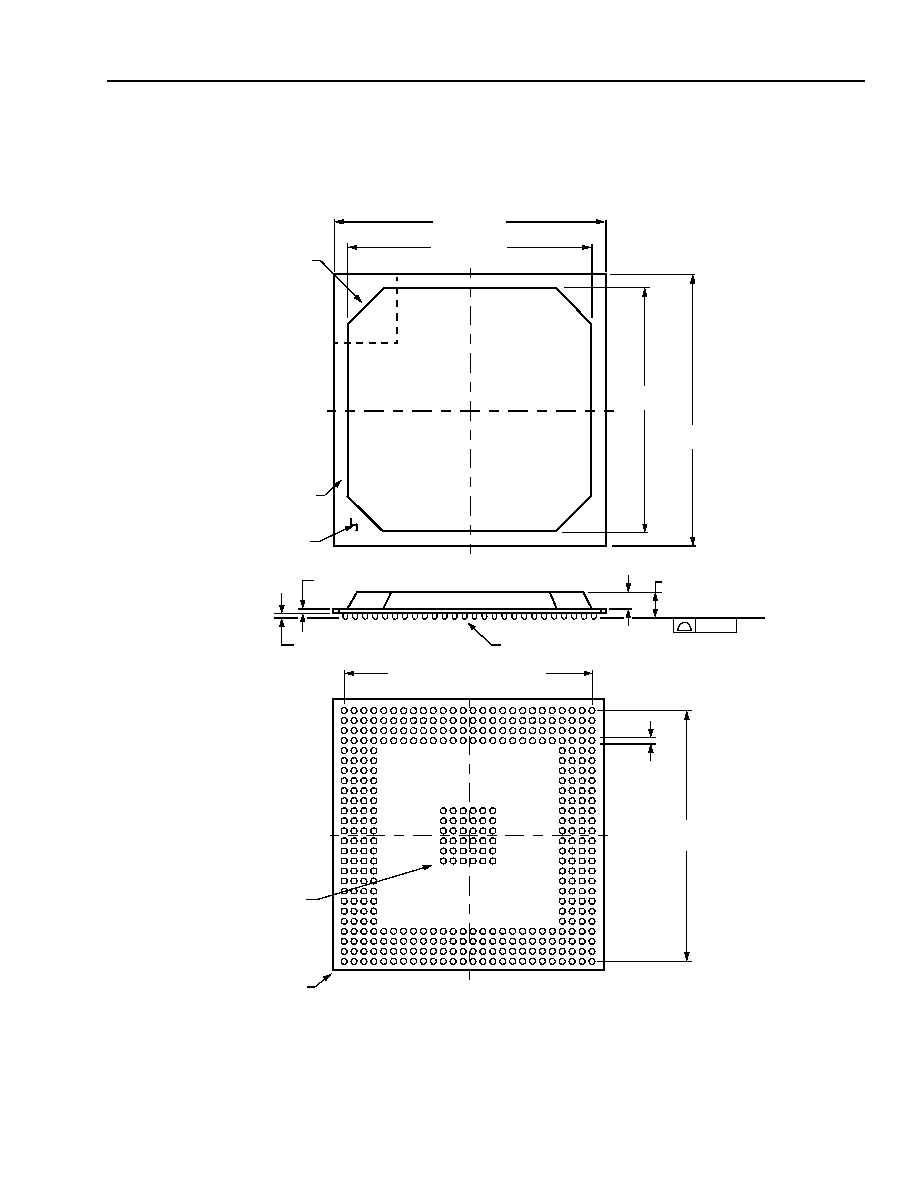
Data Sheet
June 1999
ORCA Series 2 FPGAs
Lucent Technologies Inc.
185
Package Outline Drawings
(continued)
352-Pin PBGA
Dimensions are in millimeters.
5-4407r.4
0.56
±
0.06
1.17
±
0.05
2.33
±
0.21
SEATING PLANE
SOLDER BALL
0.60
±
0.10
0.20
PWB
MOLD
COMPOUND
35.00
+0.70
≠0.00
30.00
A1 BALL
IDENTIFIER ZONE
AF
AE
AD
AC
AB
AA
Y
W
V
U
T
R
G
25 SPACES @ 1.27 = 31.75
P
N
M
L
K
J
H
1 2 3 4 5 6 7 8 9 10
12
14 16
18
22
24
26
20
11 13
15
17
21
19
23
25
F
E
D
C
B
A
CENTER ARRAY
25 SPACES
A1 BALL
0.75
±
0.15
35.00
±
0.20
30.00
+0.70
≠0.00
±
0.20
@ 1.27 = 31.75
FOR THERMAL
ENHANCEMENT
CORNER
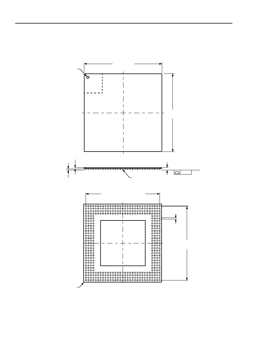
Data Sheet
ORCA Series 2 FPGAs
June 1999
186
Lucent Technologies Inc.
Package Outline Drawings
(continued)
432-Pin EBGA
Dimensions are in millimeters.
5-4409r.3
0.91
±
0.06
1.54
±
0.13
SEATING PLANE
SOLDER BALL
0.63
±
0.07
0.20
40.00
±
0.10
40.00
A1 BALL
M
D
AG
B
F
K
H
G
E
AD
L
T
J
N
AJ
C
Y
P
AH
AE
AC
AA
W
U
R
AK
AF
AB
V
AL
A
19
30
26
5
28
24
22
23
25
7
20
31
29
15
21
18
3
27
11
17
4
6
8
10
12
14 16
2
9
13
1
30 SPACES @ 1.27 = 38.10
30 SPACES
A1 BALL
0.75
±
0.15
IDENTIFIER ZONE
±
0.10
@ 1.27 = 38.10
CORNER
Data Sheet
June 1999
ORCA Series 2 FPGAs
Lucent Technologies Inc.
187
Ordering Information
OR2C12A, -4 speed grade, 240-pin shrink quad flat pack, commercial temperature.
Table 56. FPGA Voltage Options
Device
Voltage
OR2CxxA
5.0 V
OR2TxxA
3.3 V
OR2TxxB
3.3 V
Table 57. FPGA Temperature Options
Symbol
Description
Temperature
(Blank)
Commercial
0 ∞C to 70 ∞C
I
Industrial
≠40 ∞C to +85 ∞C
Table 58. FPGA Package Options
Symbol
Description
BA
Plastic Ball Grid Array (PBGA)
BC
Enhanced Ball Grid Array (EBGA)
J
Quad Flat Package (QFP)
M
Plastic Leaded Chip Carrier (PLCC)
PS
Power Quad Shrink Flat Package (SQFP2)
S
Shrink Quad Flat Package (SQFP)
T
Thin Quad Flat Package (TQFP)
OR2C12A-4 S 240
DEVICE TYPE
SPEED GRADE
PACKAGE TYPE
NUMBER OF PINS
TEMPERATURE RANGE
Example:

Data Sheet
ORCA Series 2 FPGAs
June 1999
188
Lucent Technologies Inc.
Ordering Information
(continued)
Key: C = commercial, I = industrial.
Key: C = commercial, I = industrial.
Notes:
The package options with the SQFP/SQFP2 designation in the table above use the SQFP package for all densities up to and including the
OR2C/T15A/B, while the OR2C/T26A and the OR2C/2T40A/B use the SQFP2.
The OR2TxxA and OR2TxxB series is not offered in the 304-pin SQFP/SQFP2 packages.
The OR2C40A is not offered in a 352-pin PBGA.
Table 59.
ORCA
OR2CxxA/OR2TxxA
Series
Package Matrix
Packages
84-Pin
PLCC
100-Pin
TQFP
144-Pin
TQFP
160-Pin
QFP
208-Pin
EIAJ
SQFP/
SQFP2
240-Pin
EIAJ
SQFP/
SQFP2
256-Pin
PBGA
304-Pin
EIAJ
SQFP/
SQFP2
352-Pin
PBGA
432-Pin
EBGA
M84
T100
T144
J160
S208/
PS208
S240/
PS240
BA256
S304/
PS304
BA352
BC432
OR2C/2T04A
CI
CI
CI
CI
CI
--
--
--
--
--
OR2C/2T06A
CI
CI
CI
CI
CI
CI
CI
--
--
--
OR2C/2T08A
CI
--
--
CI
CI
CI
CI
--
--
--
OR2C/2T10A
CI
--
--
CI
CI
CI
CI
--
CI
--
OR2C/2T12A
CI
--
--
--
CI
CI
CI
CI
CI
--
OR2C/2T15A
CI
--
--
--
CI
CI
CI
CI
CI
CI
OR2C/2T26A
--
--
--
--
CI
CI
--
CI
CI
CI
OR2C/2T40A
--
--
--
--
CI
CI
--
CI
CI
CI
Table 60.
ORCA
OR2TxxB
Series
Package Matrix
Packages
84-Pin
PLCC
100-Pin
TQFP
144-Pin
TQFP
160-Pin
QFP
208-Pin
EIAJ
SQFP/
SQFP2
240-Pin
EIAJ
SQFP/
SQFP2
256-Pin
PBGA
304-Pin
EIAJ
SQFP/
SQFP2
352-Pin
PBGA
432-Pin
EBGA
M84
T100
T144
J160
S208/
PS208
S240/
PS240
BA256
S304/
PS304
BA352
BC432
OR2T15B
--
--
--
--
CI
CI
CI
--
CI
--
OR2T40B
--
--
--
--
CI
CI
--
--
CI
CI

189
Lucent Technologies Inc.
Data Sheet
ORCA Series 2 FPGAs
June 1999
Index
A
Absolute Maximum Ratings, 129
Adder (see LUT Operating Modes)
Architecture
Overview, 5
PLC, 22
PIC, 25
B
Bidirectional Buffers (BIDIs), 14, 17, 18, 20, 22
(see also Routing and SLIC)
Bit Stream (see FPGA Configuration)
Bit Stream Error Checking, 47
(see also FPGA States of Operation)
Boundary Scan, 54--59
C
Clock Distribution Network, 37--39
Selecting Clock Input Pins, 39
Clock Enable (CE), 1, 5, 7, 15, 16, 24, 134
Comparator (see LUT Operating Modes)
Configuration (see FPGA States of Operation
or FPGA Configuration)
Control Inputs, 5, 7
E
Electrical Characteristics, 130
Error Checking (see FPGA Configuration)
F
5 V Tolerant I/O, 26--27, 64
FPGA Configuration
Configuration Frame Format, 43--46
Configuration Modes, 47, 158--160
Asynchronous Peripheral Mode, 49, 163
Daisy-Chaining, 51
Master Parallel Mode, 47
Master Serial Mode, 162
Slave Parallel Mode, 48, 50, 161, 166
Slave Serial Mode, 49--50, 165
Synchronous Peripheral Mode, 48, 164
Data Format, 43--45
Using
ORCA
Foundry to Generate RAM Data, 43
FPGA States of Operation, 40--43
Configuration, 41
Initialization, 40
Other Configuration Options, 43
Partial Reconfiguration, 43
Reconfiguration, 42
Start-Up, 41
G
GSR (see GSRN)
GSRN, 6, 7, 16, 37, 134
I
IEEE
Standard 1149.1, 1
(see also Boundary Scan)
Initialization (see FPGA States of Operation)
Input/Output Buffers (see PICs)
Measurement Conditions, 169
Output Buffer Characteristics, 170--172
J
JTAG (see Boundary Scan)
L
Look-up Table (LUT) Operating Modes, 7--15
Adder-Subtractor Submode, 10
Counter Submode, 11
Equality Comparators, 11
Logic Modes, 7--9
Memory Mode, 12--15
Asynchronous Memory, 12
Synchronous Memory, 13
Multiplier Submode, 11
Ripple Mode, 10
LSR, 5--7, 15--16
M
Maximum Ratings (see Absolute Maximum Ratings)
Multiplier (see LUT Operating Modes)
O
ORCA
Foundry Development System Overview, 4
Ordering Information, 189
Package Matrix, 190
Package Options, 189
Temperature Options, 189
Voltage Options, 189
Output (see PICs)
P
Package Outline Drawings, 174--186
Package Matrix, 190
Package Outline Drawings, 173
84-Pin PLCC, 174
100-Pin TQFP, 175
144-Pin TQFP, 176

Lucent Technologies Inc.
190
Data Sheet
June 1999
ORCA Series 2 FPGAs
Index
(continued)
160-Pin QFP, 177
208-Pin SQFP, 178
208-Pin SQFP2, 179
240-Pin SQFP, 180
240-Pin SQFP2, 181
256-Pin PBGA, 182
304-Pin SQFP, 183
304-Pin SQFP2, 184
352-Pin PBGA, 185
432-Pin EBGA, 186
Terms and Definitions, 173
Pin Information, 71--125
84-Pin PLCC, 71
100-Pin TQFP, 73
144-Pin TQFP, 75
160-Pin QFP, 77
208-Pin SQFP/SQFP2, 81
240-Pin SQFP/SQFP2, 86
256-Pin PBGA, 92
304-Pin SQFP/SQFP2, 99
352-Pin PBGA, 106
432-Pin EBGA Pinout, 116
Package Compatibility, 68--70
Pin Descriptions, 71
Power Dissipation, 61--65
5 V Tolerant I/O, 64
OR2CxxA, 61
OR2TxxA, 63
Programmable Function Unit (PFU), 5--16
Control Inputs, 5, 7
Operating Modes, 7--15
Latches/Flip-Flops, 15--16
Programmable Input/Output Cells (PICs), 25--31
5 V Tolerant I/O, 26
Architecture, 29--30
Inputs, 25
Outputs, 26
Open-Drain Output Option, 26
Propagation Delays, 26
Overview, 25
Zero-Hold Input, 25
Programmable Logic Cells (PLCs), 5--24
Architecture, 22--24
Latches/Flip-Flops, 15--16
PFU, 5--16
Routing, 17--24
R
RAM (see also FPGA Configuration), 17, 44, 135, 142
Dual-port, 3, 7, 13--15
Single-port, 3, 7, 12--15
Recommended Operating Conditions, 129
Reconfiguration (see FPGA States of Operation)
Routing
3-Statable Bidirectional Buffers, 17--18, 148
Clock Routing, 24, 149--153
(see also Clock Distribution Network)
Configurable Interconnect Points (CIPs), 17
Fast-Carry Routing, 24
Inter-PLC Routing Resources, 18--19
Interquad Routing, 5, 17, 32--36
Intra-PLC Routing Resources, 18
Minimizing Routing Delay, 20
PLC Routing, 17--24, 34
Programmable Corner Cell Routing, 37
PIC Routing, 27--31
S
Boundary Scan, 54≠59
Global 3-State Control (TS_ALL), 37, 66
Global Set/Reset (GSRN), 7, 16, 37
Internal Oscillator, 37
Readback Logic, 37
Start-up, 41 (see also FPGA States of Operation)
Subtractor (see LUT Operating Modes)
System Clock (see Clock Distribution Network)
T
3-state (see Bidirectional Buffers, TS_ALL)
Timing Characteristics, 132≠168
Asynchronous Peripheral Configuration Mode, 163
Boundary-Scan Timing, 168
Clock Timing, 149
General Configuration Mode Timing, 158
Master Parallel Configuration Mode, 162
Master Serial Configuration Mode, 161
PFU Timing, 132
PIO Timing, 154
PLC Timing, 148
Readback Timing, 167
Slave Parallel Configuration Mode, 166
Slave Serial Configuration Mode, 165
Tolerant I/O, 26 (see also 5 V Tolerant I/O)
TS_ALL, 1, 37, 66
U--Z
Zero-hold Inputs, 25

Data Sheet
June 1999
ORCA Series 2 FPGAs
Lucent Technologies Inc.
191
Notes

Lucent Technologies Inc. reserves the right to make changes to the product(s) or information contained herein without notice. No liability is assumed as a result of their use or application. No
rights under any patent accompany the sale of any such product(s) or information.
ORCA is a registered trademark of Lucent Technologies Inc. Foundry is a trademark of Xilinx Inc.
Copyright © 1999 Lucent Technologies Inc.
All Rights Reserved
June 1999
DS99-094FPGA (Replaces DS98-022FPGA)
For additional information, contact your Microelectronics Group Account Manager or the following:
INTERNET:
http://www.lucent.com/micro or for FPGA information, http://www.lucent.com/orca
E-MAIL:
docmaster@micro.lucent.com
N. AMERICA:
Microelectronics Group, Lucent Technologies Inc., 555 Union Boulevard, Room 30L-15P-BA, Allentown, PA 18103
1-800-372-2447, FAX 610-712-4106 (In CANADA: 1-800-553-2448, FAX 610-712-4106)
ASIA PACIFIC: Microelectronics Group, Lucent Technologies Singapore Pte. Ltd., 77 Science Park Drive, #03-18 Cintech III, Singapore 118256
Tel. (65) 778 8833, FAX (65) 777 7495
CHINA:
Microelectronics Group, Lucent Technologies (China) Co., Ltd., A-F2, 23/F, Zao Fong Universe Building, 1800 Zhong Shan Xi Road, Shanghai
200233 P. R. China Tel. (86) 21 6440 0468, ext. 316, FAX (86) 21 6440 0652
JAPAN:
Microelectronics Group, Lucent Technologies Japan Ltd., 7-18, Higashi-Gotanda 2-chome, Shinagawa-ku, Tokyo 141, Japan
Tel. (81) 3 5421 1600, FAX (81) 3 5421 1700
EUROPE:
Data Requests: MICROELECTRONICS GROUP DATALINE: Tel. (44) 1189 324 299, FAX (44) 1189 328 148
Technical Inquiries: GERMANY: (49) 89 95086 0 (Munich), UNITED KINGDOM: (44) 1344 865 900 (Ascot),
FRANCE: (33) 1 40 83 68 00 (Paris), SWEDEN: (46) 8 594 607 00 (Stockholm), FINLAND: (358) 9 4354 2800 (Helsinki),
ITALY: (39) 02 6608131 (Milan), SPAIN: (34) 1 807 1441 (Madrid)