OTi-6828
FLASH DISK CONTROLLER
Ours Technology Inc.
OTi
Description
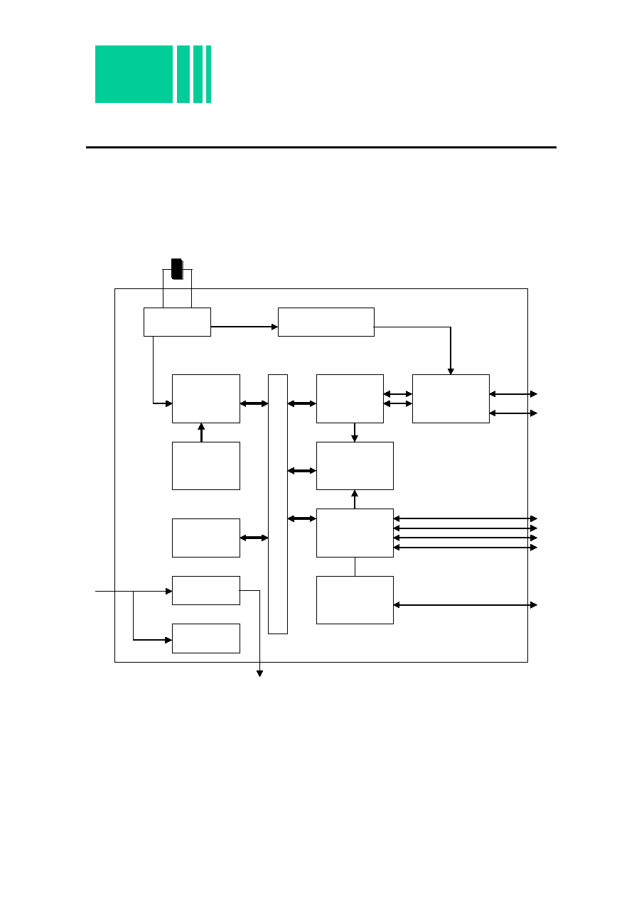
The flash disk controller (OTi_6828) is a disk controller used to make a linear flash device array
look likes a normal disk, hiding the flash related problems with erasing.
The OTi_6828 is a controller with USB interface. The USB interface is for full speed operation
(12Mb/s). It conforms to USB Specification, Version 1.1. The USB transceiver is embedded in this
controller. With stable slew-rate control, the controller reduces EMI.
The OTi_6828 has a Phase Lock Loop (PLL) embedded. The PLL provides all clocks needed in
this controller. It needs an externally provided clock operating in 14.318MHz.
The OTi_6828 has integrated the regulator for 5V input and 3.3V output. It also supports voltage
detector for power on reset.
The OTi_6828 can control up to 4 pieces of NAND flash memory. The flash capacity can be 32M
bits up to 1G bits. And these chips can be any combination. It has been optimized to support Toshiba
and Samsung flash memory designs. It also supports Samsung's K9F and K9W Series flash. The
controller has write-protected ability to prevent writing data to flash. The controller has a led control
pin. It has three operation modes: suspend (off), active (fast) and idle (twinkle) mode. For read/write
operation, the controller can achieve 1,000kB/920kB throughput. Comprehensive application with
Windows OS is available.
This controller can operate in Win XP, Win2000, Windows Me, and Mac OS without any driver
installation.
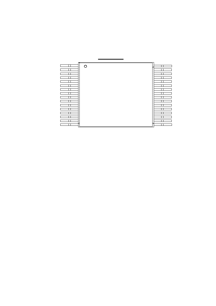
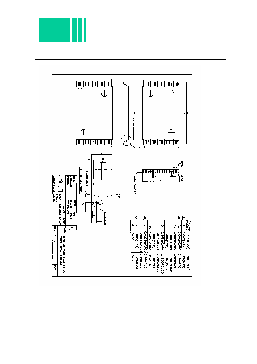
The OTi_6828 is available in cost-saving 32-pin TSOP package.
Features
· Flash controller with full-speed USB interface
· Integrated 5V/3.3V regulator, USB bus power supply capability
· USB Specification Compliance
-- Conforms to USB Specification, Version 1.1
· Integrated USB transceiver
-- Dynamic feedback control
-- Stable slew rate, independent of external loading
· RISC micro-controller
-- High-performance RISC architecture
-- Single cycle instruction execution
· 14.318 MHz external clock

· Integrated PLL
· Integrated Power On Reset (POR)
· Support up to 4 pieces of NAND Flash memory with write-protected ability
· Support Toshiba and Samsung's K9K series flash
· Support Samsung's K9F and K9W series flash
· Support wear-leveling
· Higher reliability: ECC on the fly
· Automatic bad block management
· Supported OS:
Win XP, Win2000, Windows ME, Linux 2.4 above, and MAC OS 9.0 & higher
Win 98/Win98SE driver available
Mac 8.6 mass storage driver available from Apple
Multiple LUN Windows driver is available
· LED indication:
Programmable through Mass Production Toolset
· Configurable Vendor ID/Product ID (VID/PID)
· Performance: Read (1,000kBytes/s) , Write (920kBytes/s) Max.
· Small form factor - standard 32-pin TSOP package
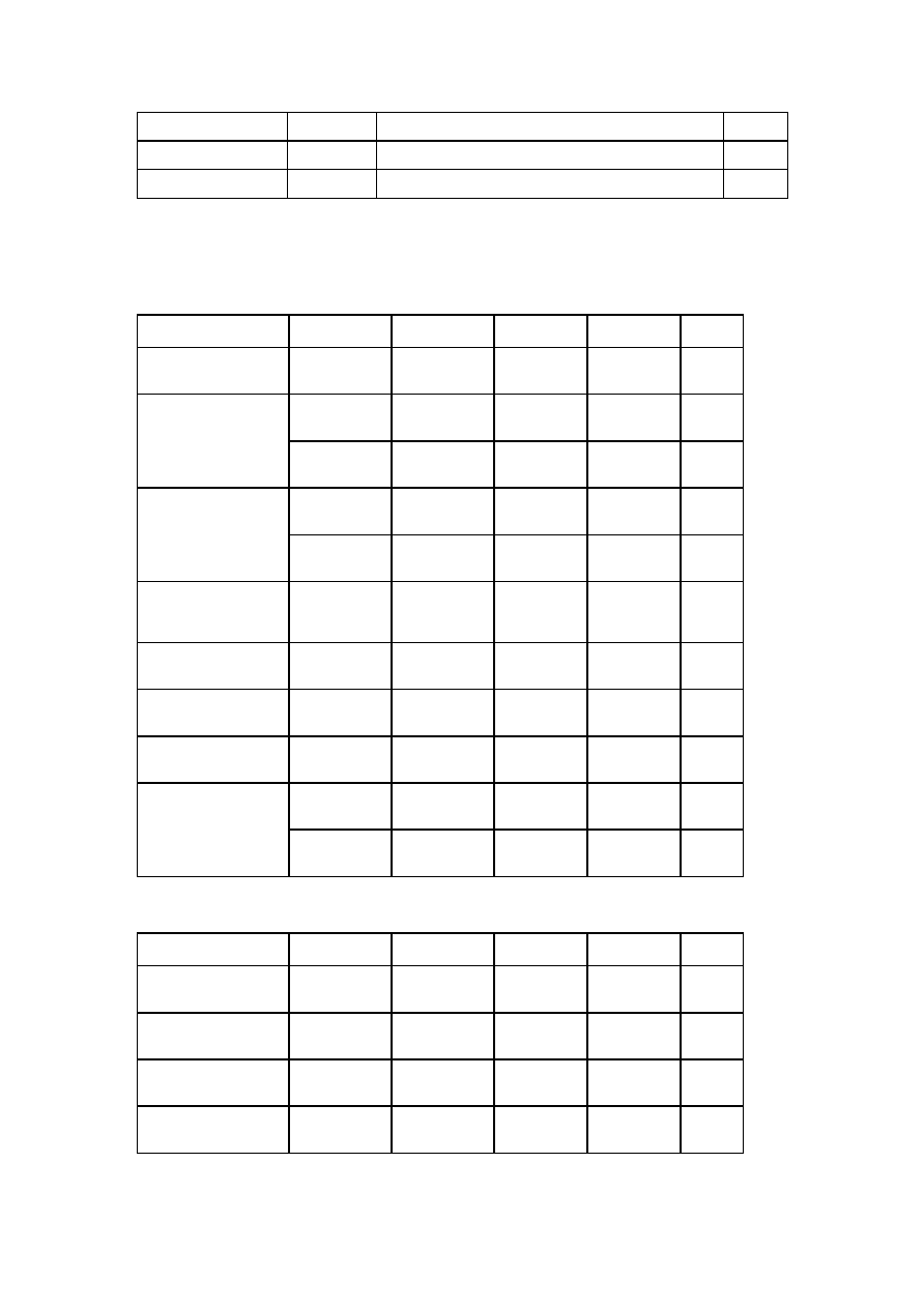
FL_CE1
O
Flash Chip Enable Chip 1
30
FL_CE2
O
Flash Chip Enable Chip 2
31
FL_CE3
O
Flash Chip Enable Chip 3
32
D.C. Characters
DC Characteristics-1 (Ta=0
o
C to +70
o
C, Vcc = 3.3V ±10%)
Parameter Symbol
MIN
TYP
MAX
Unit
Power Supply
VDD5V
4.5 5 5.5
V
VIH
0.7x VDD
--
5
V
Input Voltage
VIL
-0.3
--
0.2 x VDD
V
VOH
VDD-0.4 --
-- V
Output Voltage
VOL
-- --
0.4
V
Input leakage current
(*2)
ILK
-1 -- 1
uA
Working Current
IRW
-- 20 --
mA
Operating Temperature
Ta
0 70
°C
Storage Temperature
Ts
-55
+150
°C
IOH
-- 4 --
mA
IO output current
IOL
-- 4 --
mA
A.C. Characters
Parameter Symbol
MIN
TYP
MAX
Unit
Input rising delay
TPIlh
0.35(2PF) 0.4(4PF) 0.54(8PF) ns
Input falling delay
TPIhl
0.46(2PF) 0.53(4PF) 0.64(8PF) ns
Output rising delay
TPOlh
1.35(10PF) 1.97(30PF)
2.59(50pF) ns
Output falling delay
TPOhl
1.61(10PF) 2.41(30PF)
3.21(50pF) ns