 | –≠–ª–µ–∫—Ç—Ä–æ–Ω–Ω—ã–π –∫–æ–º–ø–æ–Ω–µ–Ω—Ç: OV6130 | –°–∫–∞—á–∞—Ç—å:  PDF PDF  ZIP ZIP |

Advanced Information
Preliminary
OV6630/OV6130
OV6630 SINGLE-CHIP CMOS CIF COLOR DIGITAL CAMERA
OV6130 SINGLE-CHIP CMOS CIF B&W DIGITAL CAMERA
OmniVision Technologies, Inc. 930 Thompson Place Sunnyvale, CA 94086 U.S.A.
Tel: (408) 733-3030 Fax: (408) 733-3061
e-mail:
info@ovt.com
Website: http://www.ovt.com
Version 1.0, March 4, 2000
Features
101,376 pixels, 1/4" lens, CIF/QCIF format
Progressive scan read out
Data format - YCrCb 4:2:2, GRB 4:2:2, RGB Raw Data
8/16 bit video data: ITU-601, ITU-656, ZV port
Wide dynamic range, anti-blooming, zero smearing
Electronic exposure/gain/white balance control
Image enhancement - brightness, contrast, gamma,
saturation, sharpness, window, etc.
Internal/external synchronization
Frame exposure/line exposure option
3.3-Volt operation, low power dissipation
-
< 20 mA active power
-
< 10
µ
A in power-save mode
Gamma correction (0.45/0.55/1.00)
I
2
C programmable (400 kb/s):
-
Color saturation, brightness, contrast, white balance,
exposure time, gain
General Description
The OV6630 (color) and OV6130 (black and white) CMOS Im-
age sensors are single-chip video/imaging camera devices
designed to provide a high level of functionality in a single,
small-footprint package. Both devices incorporate a 352 x 288
image array capable of operating up to 60 frames per second
image capture. Proprietary sensor technology utilizes advanced
algorithms to cancel Fixed Pattern Noise (FPN), eliminate
smearing, and drastically reduce blooming. All needed camera
functions including exposure control, gamma, gain, white
balance, color matrix, windowing, and more, are programmable
through an I
2
C interface. Both devices can be programmed to
provide image output in 4-bit, 8-bit or 16-bit digital formats.
Applications include: Video Conferencing, Video Phone, Video
Mail, Still Image, and PC Multimedia.
8
48
35
VRCAP1
24
SGND
31
17
DEGND
34
15
DEVDD
Y4/CS1
Y3/RGB
10
AVDD
42
20
43
7
27
Y5/SHARP
47
36
26
14
ASUB
OV6630/
OV6130
6
41
MULT
UV2/QCIF
Y6/CS2
29
FODD/CLK
11
3
33
IICB
UV3
XCLK1
HREF/VSFRAM
SCL
SVDD
DOVDD
22
Y7/CS0
46
UV5/MIR
V0/CBAR
Y2/G2X
VSYNC/CSYS
23
SDA
Y1
16
2
40
PCLK/PWDB
37
FREX
9
DGND
45
28
RESET
CHSYNC/BW
19
32
AGND
HVDD
5
1
38
21
UV0/GAMMA
UV7/B8
13
30
VTO
12
DOGND
ADVDD
25
44
XCLK2
UV6/ABKEN
VcCHG
18
UV1/CC656
39
ADGND
4
DVDD
AGCEN
UV4
PWDN
Figure 1. OV6630/OV6130 Pin Assignments
Array Element(CIF)
(QCIF)
356x292
(176x144)
Pixel Size
9
µ
m x 8.2
µ
m
Image Area
3.1mm x 2.5mm
Max Frames/Sec
Up to 60 FPS
Electronics
Exposure
Up to 500:1 (for selected
FPS)
Scan Mode
Progressive
Gamma Correction
0.45/0.55/1.0
Min. Illumination
(3000K)
OV6630 - < 3lux @ f1.2
OV6130 - < 0.5lux @ f1.2
S/N Ration
> 48 dB
(AGC off, Gamma=1)
FPN
< 0.03% V
PP
Dark Current
< 0.2nA/cm
2
Dynamic Range
> 72 dB
Power Supply
2.7
-
3.6VDC
5VDC/3.3VDC (DIO)
Power
Requirements
< 20mA active
< 10
µ
A Standby
Package
48 pin LCC
Note: Outputs UV0-UV7 are not available on the OV6130. The inputs associated
with these respective pins are still functional.

SINGLE IC CMOS COLOR AND B/W DIGITAL CAMERAS
March 4, 2000
Version 1.0
2
Table 1. Pin Description
Pin No.
Name
Pin Type
Function/Description
01 SVDD
V
IN
Array power (+3.3VDC)
02 RESET
Function
(Default=0)
Chip reset, active high
03 AGCEN
Function
(Default=0)
Automatic Gain Control (AGC) selection
"0" ≠ Disable AGC
"1" ≠ Enable AGC
Note: This function is disabled when OV6630/OV6130 sensor is configured in I
2
C mode.
04 FREX
Function
(Default=0)
Frame exposure control
"0" ≠ Disable frame exposure control
"1" ≠ Enable frame exposure control
05 HVDD
V
REF
(4V)
Charge pump voltage. Connect to ground through 10
µ
F capacitor.
06 ASUB
V
IN
Analog substrate voltage.
07 AGND
V
IN
Analog
ground
08 AVDD
V
IN
Analog power supply (+3.3VDC)
09 PWDN
Function
(Default=0)
Power down mode selection.
"0" ≠ Normal mode.
"1" ≠ Power down mode.
10 VRCAP1
V
REF
(1.5V)
Array reference. Connect to ground through 0.1
µ
F capacitor.
11 V
C
CHG V
REF
(2.7V)
Internal voltage reference. Connect to ground through 1
µ
F capacitor.
12 IICB
Function
(Default=0)
I
2
C enable selection.
"0" ≠ Enable I
2
C
"1" ≠ Enable auto-control mode
13
VTO
O
Luminance composite signal output (black/white in PAL standard).
14 ADVDD
V
IN
Analog power supply (+3.3VDC)
15 ADGND
V
IN
Analog signal ground
16
VSYNC/CSYS
I/O
Vertical sync output. At power up, read as CSYS.
17
FODD/CLK
I/O
Field ID FODD output or main clock output
18
HREF/VSFRAM I/O
HREF output. At power up, read as VSFRAM
19
*
UV7/B8
I/O
Bit 7 of U video component output. At power up, sampled as B8.
* Note: Output UV7 is not available on the OV6130 sensor.
20
*
UV6/ABKEN
I/O
Bit 6 of U video component output. At power up, sampled as ABKEN.
* Note: Output UV6 is not available on the OV6130 sensor.
21
*
UV5/MIR
I/O
Bit 5 of U video component output. At power up, sampled as MIR.
* Note: Output UV5 is not available on the OV6130 sensor.
22
*
UV4
I/O
Bit 4 of U video component output.
* Note: Output UV4 is not available on the OV6130 sensor.
23
*
UV3
I/O
Bit 3 of U video component output.
* Note: Output UV3 is not available on the OV6130 sensor.
24
*
UV2/QCIF
I/O
Bit 2 of U video component output. At power up, sampled as QCIF.
* Note: Output UV2 is not available on the OV6130 sensor.
25
*
UV1/CC656
I/O
Bit 1 of U video component output. At power up, sampled as CC656.
* Note: Output UV1 is not available on the OV6130 sensor.
26
*
UV0/GAMMA
I/O
Bit 0 of U video component output. At power up, sampled as GAMMA.
* Note: Output UV0 is not available on the OV6130 sensor.
27
XCLK1
I
Crystal clock input
28
XCLK2
O
Crystal clock output
29 DVDD
V
IN
Digital power supply (+3.3VDC)
30 DGND
V
IN
Digital
ground
31 DOGND
V
IN
Digital interface output buffer ground
32 DOVDD
V
IN
Digital interface output buffer power supply (+3.3VDC or 5VDC)
33
PCLK/PWDB
I/O
PCLK output. At power up sampled as PWDB.
34
Y7/CS0
I/O
Bit 7 of Y video component output. At power up, sampled as CS0.
35
Y6/CS2
I/O
Bit 6 of Y video component output. At power up, sampled as CS2.
36
Y5/SHARP
I/O
Bit 5 of Y video component output. At power up, sampled as SHAPR.
37
Y4/CS1
I/O
Bit 4 of Y video component output. At power up, sampled as CS1.
38
Y3/RGB
I/O
Bit 3 of Y video component output. At power up, sampled as RGB.

SINGLE IC CMOS COLOR AND B/W DIGITAL CAMERAS
March 4, 2000
Version 1.0
3
39
Y2/G2X
I/O
Bit 2 of Y video component output. At power up, sampled as G2X.
40
Y1
I/O
Bit 1 of Y video component output.
41
Y0/CBAR
I/O
Bit 0 of Y video component output. At power up, sampled as CBAR.
42
CHSYNC/BW
I/O
CHSYNC output. At power up, sampled as BW.
43 DEGND
V
IN
Decoder
ground.
44 DEVDD
V
IN
Decoder power supply (+3.3VDC)
45 SCL
I
I
2
C serial interface clock input.
46 SDA
I/O
I
2
C serial interface data input and output.
47 MULT
Function
(Default=0)
I
2
C slave selection
"0" ≠ Select single slave ID.
"1" ≠ Enable multiple (8) slaves.
48 SGND
V
IN
Array
ground
1 Function
Description
(Note: References to color features do not apply to the OV6130 B&W Digital Image Sensor.)
1.1 Overview
Referring to Figure 2 below, the OV6630 sensor includes a 356 x 292
resolution image array, an analog signal processor, dual 8-bit A/D
converters, analog video multiplexer, digital data formatter, video
port, I
2
C interface, registers, and digital controls that include timing
block, exposure control, black level control, and white balance.
The OV6630/OV6130 sensor is a º inch CMOS imaging device. The
sensor contains approximately 101,376 pixels. Its design is based on a
field integration read-out system with line-by-line transfer and an
electronic shutter with a synchronous pixel read out scheme. The
color filter of the sensor consists of a primary color RG/GB array
arranged in line-alternating fashion.
B
Cr
Column Sense Amp
R
PR
OG
1/2
AG
CE
N
A/D
MUX
II
CB
Cb
FZ
EX
Y[7:0]
UV[7:0]
Formatter
Exposure
Control
SC
L
GA
MMA
registers
Ro
w
S
el
ec
t
D
ENB
(356x292)
Image Array
A/D
Exposure
Detect
SD
A
X
CLK
1
Analog
Processing
WB
Detect
AW
B
Video Timing
Generator
Video
port
Y
AW
BT
H/
AW
BT
M
WB
Control
VTO
G
MUX
I2C
Interface
HRE
F
PCL
K
V
SYN
C
FOD
D
CH
SYN
C
MI
R
Figure 2. OV6630/OV6130 CMOS Image Sensor Block Diagram

SINGLE IC CMOS COLOR AND B/W DIGITAL CAMERAS
March 4, 2000
Version 1.0
4
1.2 Analog Processor Circuits
1.2.1 Overview
The image is captured by the 356 x 292 pixel image array and routed
to the analog processing section where the majority of signal
processing occurs. This block contains the circuitry that performs
color separation, color correction, automatic gain control (AGC),
gamma correction, color balance, black level calibration, "knee"
smoothing, aperture correction, controls for picture luminance and
chrominance, and anti-alias filtering. The analog video signals are
based on the following formula:
Y = 0.59G + 0.31R + 0.11B
U = R ≠ Y
V = B ≠ Y
Where R,G,B are the equivalent color components in each
pixel.
YCrCb format is also supported, based on the formula below:
Y = 0.59G + 0.31R + 0.11B
Cr = 0.713 (R ≠ Y)
Cb = 0.564 (B ≠ Y)
The YCrCb/RGB data signal from the analog processing section is
fed to two on-chip 8-bit analog-to-digital (A/D) converters: one for
the Y/RG channel and one shared by the CrCb/BG channels. The
converted data stream is further conditioned in the digital formatter.
The processed signal is delivered to the digital video port through the
video multiplexer which routes the user-selected 16-, 8-, or 4-bit
video data to the correct output pins.
The on-chip 8-bit A/D operates up to 9 MHz, and fully synchronous
to the pixel rate. Actual conversion rate is related to the frame rate.
A/D black-level calibration circuitry ensures:
The black level of Y/RGB is normalized to a value of 16
The peak white level is limited to 240
CrCb black level is 128
CrCb Peak/bottom is 240/16
RGB raw data output range is 16/240
(Note: Values 0 and 255 are reserved for sync flag)
1.2.2 Image
Processing
The algorithm used for the electronic exposure control is based on the
brightness of the full image. The exposure is optimized for a "normal"
scene that assumes the subject is well lit relative to the background. In
situations where the image is not well lit, the automatic exposure
control (AEC) white/black ratio may be adjusted to suit the needs of
the application.
Additional on-chip functions include
AGC that provides a gain boost of up to 24dB
White balance control that enables setting of proper color
temperature and can be programmed for automatic or manual
operation.
Separate saturation, brightness, contrast, and sharpness
adjustments allow for further fine-tuning of the picture quality
and characteristics.
The OV6630 image sensor also provides control over the White
Balance ratio for increasing/decreasing the image field Red/Blue
component ratio. The sensor provides a default setting that may be
sufficient for many applications.
1.2.3 Windowing
The windowing feature of the OV6630/OV6130 image sensors allows
user-definable window sizing as required by the application. Window
size setting (in pixels) ranges from 2 x 2 to 356 x 292, and can be
positioned anywhere inside the 356 x 292 boundary. Note that
modifying window size and/or position does not change frame or data
rate. The OV6630/OV6130 imager alters the assertion of the HREF
signal to be consistent with the programmed horizontal and vertical
region. The default output window is 352 x 288.
1.2.4
Zoom Video Port (ZV)
The OV6630/OV6130 image sensor includes a Zoom Video (ZV)
function that supports standard ZV Port interface timing. Signals
available include VSYNC, CHSYNC, PCLK and 16-bit data bus:
Y[7:0] and UV[7:0]. The rising edge of PCLK clocks data into the ZV
port. See Figure 3. Zoom Video Port Timing below.

SINGLE IC CMOS COLOR AND B/W DIGITAL CAMERAS
March 4, 2000
Version 1.0
5
VSYNC
PCLK
Y[7:0]/UV[7:0]
HREF
Horizontal Timing
VSYNC
Even Field 1 (FODD=0)
Odd Field 1 (FODD=1)
t8
t8
t6
t7
t5
t4
t2
t1
t3
2
1
352
351
Valid Data
T
VS
T
LINE
T
VE
1 Line
Y[7:0]/UV[7:0]
Vertical Timing
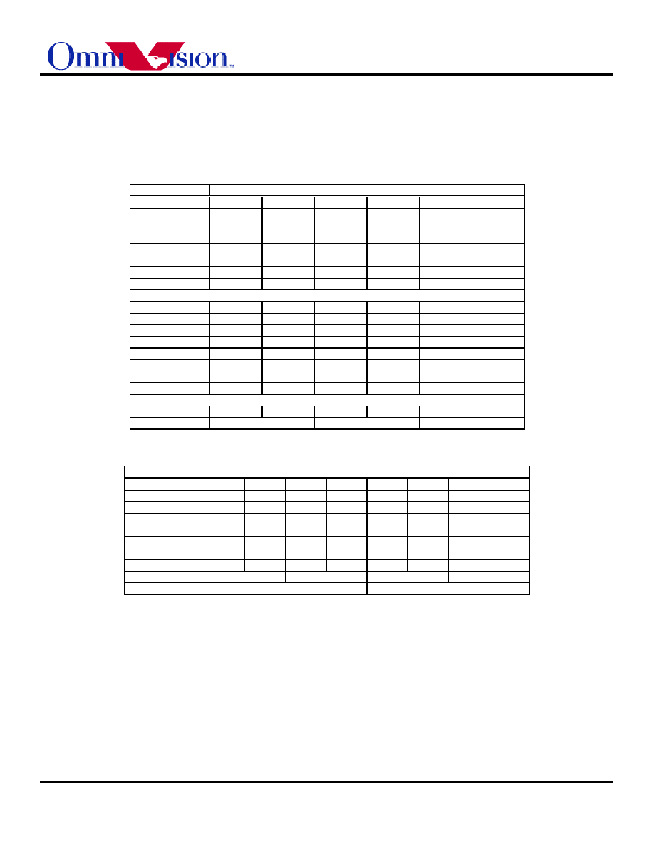
Figure 3. Zoom Video Port Timing
Notes:
1. Zoom Video Port format output signal includes:
VSYNC: Vertical sync pulse.
HREF: Horizontal valid data output window.
PCLK: Pixel clock used to clock valid data and CHSYNC into Zoom V Port. Default frequency is 8.86MHz when use
17.73MHz as system clock. Rising edge of PCLK is used to clock the 16 Bit data.
Y[7:0]: 8 Bit luminance data bus.
UV[7:0]: 8 Bit chrominance data bus.
2. All timing parameters are provided in Table 13. Zoom Video Port AC Parameters.
1.2.5 QCIF
Format
A QCIF mode is available for applications where higher resolution
image capture is not required. Only half of the pixel rate is required
when programmed in this mode. Default resolution is 176 x 144
pixels and can be programmed for other resolutions. Refer to Table 7.
QCIF Digital Output Format (YUV beginning of line) and Table 8.
QCIF Digital Output Format (RGB raw data beginning of line) for
further information.
1.2.6 Video
Output
The video output port of the OV6630/OV6130 image sensors
provides a number of output format/standard options to suit many
different application requirements. Table 2. Digital Output Format,
below, indicates the output formats available. These formats are user
programmable through the I
2
C interface (See I2C Bus Protocol
Format).

SINGLE IC CMOS COLOR AND B/W DIGITAL CAMERAS
March 4, 2000
Version 1.0
6
The OV6630/OV6130 imager supports both ITU-601 and ITU-656
output formats in the following configurations (See Table 3. 4:2:2 16-
bit Format for further details):
-
16-bit, 4:2:2 format
(This mode complies with the 60/50 Hz ITU-601 timing
standard. See Table 3. 4:2:2 16-bit Format below)
-
8-bit data mode
(In this mode, video information is output in Cb Y Cr Y
order using the Y port only and running at twice the pixel
rate during which the UV port is inactive. See Table 4. 4:2:2
8-bit Format below)
-
4-bit nibble mode
(In the nibble mode, video output data appears at bits Y4-
Y7. The clock rate for the output runs at twice the normal
output speed when in B/W mode, and 4 times the normal
output speed in when in color mode.)
-
704 x 288 format
(When programmed in this mode, the pixel clock is doubled
and the video output sequence is Y
0
Y
0
Y
1
Y
1
∑∑∑
and
U
0
U
0
V
0
V
0
∑∑∑
. See Figure 4. Pixel Data Bus (YUV Output)
below.)
The OV6630/OV6130 imager provides VSYNC, HREF, PCLK,
FODD, and CHSYNC as standard output video timing signals.
The OV6630/OV6130 imager can also be programmed to provide
RGB raw data in 16-bit, 8-bit, and 4-bit format. The output sequence
is matched to the OV6630 color filter pattern (See Figure 5. Pixel
Data Bus (RGB Output) below):
≠
Y channel output sequence is G R G R
≠
UV channel output sequence is B G B G
The video output appears in Y channel only and the UV channel is
disabled in 8-bit RGB raw data. The output sequence is B G R G.
In RGB raw data ITU-656 modes, the OV6630/OV6130 imager
asserts SAV (Start of Active Video) and EAV (End of Active Video)
to indicate the beginning and the ending of HREF window. As a
result, SAV and EAV change with the active pixel window. The 8-bit
RGB raw data is also accessible without SAV and EAV information.
The OV6630/OV6130 imager offers flexibility in YUV output format.
The device may be programmed as standard YUV 4:2:2. The device
may also be configured to "swap" the U V sequence. When swapped,
the UV channel output sequence in the 16-bit configuration becomes:
-
V U V U
∑∑∑
.
The 8-bit configuration becomes:
-
V Y U Y
∑∑∑
.
The third format available in the 8-bit configuration is the Y/UV
sequence swap:
-
Y U Y V
∑∑∑
.
The single-chip camera can be configured for use as a black and white
image device. The vertical resolution is higher than in color mode.
Video data output is provided at the Y port and the UV port is tri-
stated. The data (Y/RGB) rate is equivalent to 16-bit in color mode.
The MSB and LSB of Y/UV or RGB output can be reversed. Y7 is
MSB and Y0 is LSB in the default setting. Y7 becomes LSB and Y0
becomes MSB in the reserve order configuration. Y2-Y6 are also
reversed appropriately.
Table 2. Digital Output Format
Resolution
Pixel Clock
352 x 288
704 x 288
176 x 144
16-bit
Y Y Y
8-bit
Y Y Y
ITU-656 Y Y Y
YUV 4:2:2
Nibble
Y Y Y
16-bit
Y Y Y
8-bit
Y Y Y
ITU-656
1
Y Y Y
RGB
Nibble
Y Y Y
16-bit
Y/UV swap
2
8-bit
Y Y Y
YUV
3
Y Y Y
U/V swap
RGB
4
Y Y Y
16-bit
Y Y Y
YG
8-bit
16-bit Y
One Line
8-bit
MSB/LSB
swap
Y Y Y
Note:
("Y" indicates mode/combination is supported by OV6630/OV6130)
1. Output is 8-bit in RGB ITU-656 format. SAV and EAV are inserted at the beginning and ending of HREF, which
synchronize the acquisition of VSYNC and HSYNC. 8-bit data bus configuration (without VSYNC and
CHSYNC) can provide timing and data in this format.
SINGLE IC CMOS COLOR AND B/W DIGITAL CAMERAS
March 4, 2000
Version 1.0
7
2. Y/UV swap is valid in 8-bit only. Y channel output sequence is Y U Y V
∑∑∑
3. U/V swap means UV channel output sequence swap in YUV format, i.e., V U V U
∑∑∑
for 16 bit and V Y U Y
∑∑∑
for 8-bit.
4. U/V swap means neighbor row B R output sequence swap in RGB format. Refer to RGB raw data output format
for further details.
Table 3. 4:2:2 16-bit Format
Data Bus
Pixel Byte Sequence
Y7
Y7 Y7 Y7 Y7 Y7 Y7
Y6
Y6 Y6 Y6 Y6 Y6 Y6
Y5
Y5 Y5 Y5 Y5 Y5 Y5
Y4
Y4 Y4 Y4 Y4 Y4 Y4
Y3
Y3 Y3 Y3 Y3 Y3 Y3
Y2
Y2 Y2 Y2 Y2 Y2 Y2
Y1
Y1 Y1 Y1 Y1 Y1 Y1
Y0
Y0 Y0 Y0 Y0 Y0 Y0
UV7
UV7 UV7 UV7 UV7 UV7 UV7
UV6
UV6 UV6 UV6 UV6 UV6 UV6
UV5
UV5 UV5 UV5 UV5 UV5 UV5
UV4
UV4 UV4 UV4 UV4 UV4 UV4
UV3
UV3 UV3 UV3 UV3 UV3 UV3
UV2
UV2 UV2 UV2 UV2 UV2 UV2
UV1
UV1 UV1 UV1 UV1 UV1 UV1
UV0
UV0 UV0 UV0 UV0 UV0 UV0
Y
Frame
0 1 2 3 4 5
UV Frame
0
2
4
Table 4. 4:2:2 8-bit Format
Data Bus
Pixel Byte Sequence
Y7
U7 Y7 V7 Y7 U7 Y7 V7
Y6
U6 Y6 V6 Y6 U6 Y6 V6
Y5
U5 Y5 V5 Y5 U5 Y5 V5
Y4
U4 Y4 V4 Y4 U4 Y4 V4
Y3
U3 Y3 V3 Y3 U3 Y3 V3
Y2
U2 Y2 V2 Y2 U2 Y2 V2
Y1
U1 Y1 V1 Y1 U1 Y1 V1
Y0
U0 Y0 V0 Y0 U0 Y0 V0
Y
Frame 0 1 2 3
UV Frame
0 1
2 3

SINGLE IC CMOS COLOR AND B/W DIGITAL CAMERAS
March 4, 2000
Version 1.0
8
Y[7:0]
PCLK
HREF
UV[7:0]
Y[7:0]
PCLK
HREF
Pixel Data 16-bit Timing
(PCLK rising edge latches data bus)
10
Y
Y
10
80
U
V
80
T
CLK
T
SU
T
HD
Repeat for all data bytes
Pixel Data 8-bit Timing
(PCLK rising edge latches data bus)
U
Y
80
10
10
80
V
Y
10
T
CLK
T
SU
T
HD
Repeat for all data bytes
Note: T
CLK
is pixel clock period.. T
CLK
=112ns for 16-bit output and T
CLK
=56ns for 8-bit output if the system
clock is 17.73MHz. T
SU
is the setup time of HREF. The maximum is 15ns. T
HD
is the hold time of HREF.
The maximum is 15ns.
Figure 4. Pixel Data Bus (YUV Output)
SINGLE IC CMOS COLOR AND B/W DIGITAL CAMERAS
March 4, 2000
Version 1.0
9
B
Y[7:0]
PCLK
HREF
UV[7:0]
Y[7:0]
PCLK
HREF
Pixel Data 16-bit Timing
(PCLK rising edge latches data bus)
10
G
R
10
10
B
G
10
T
CLK
T
SU
T
HD
Repeat for all data bytes
Pixel Data 8-bit Timing
(PCLK rising edge latches data bus)
G
10
10
10
10
R
G
10
T
CLK
T
SU
T
HD
Repeat for all data bytes
Note: T
CLK
is pixel clock period.. T
CLK
=112ns for 16-bit output and T
CLK
=56ns for 8-bit output if the system
clock is 17.73MHz. T
SU
is the setup time of HREF. The maximum is 15ns. T
HD
is the hold time of HREF.
The maximum is 15ns.
Figure 5. Pixel Data Bus (RGB Output)

SINGLE IC CMOS COLOR AND B/W DIGITAL CAMERAS
March 4, 2000
Version 1.0
10
The default U/UV channel output port relation before MSB/LSB swap
Table 5. Default Output Sequence
MSB
LSB
Output
port
Y7 Y6 Y5 Y4 Y3 Y2 Y1 Y0
Internal
output
data Y7 Y6 Y5 Y4 Y3 Y2 Y1 Y0
The relation after MSB/LSB swap changes to
Table 6. Swapped MSB/LSB Output Sequence
MSB
LSB
Output
port
Y7 Y6 Y5 Y4 Y3 Y2 Y1 Y0
Internal
output
data Y0 Y1 Y2 Y3 Y4 Y5 Y6 Y7
Table 7. QCIF Digital Output Format (YUV beginning of line)
Pixel
# 1 2 3 4 5 6 7 8
Y
Y0 Y1 Y2 Y3 Y4 Y5 Y6 Y7
UV
U0, V0
U1, V1
U2, V2
U3, V3
U4, V4
U5, V5
U6, V6
U7, V7
-
Y channel output Y2 Y3 Y6 Y7 Y10 Y11
∑∑∑
-
UV channel output U2 V3 U6 V7 U10 V11
∑∑∑
-
Half (176 pixels) data are outputted every line and only half line data (every other line, total 144 lines) in one frame.
Table 8. QCIF Digital Output Format (RGB raw data beginning of line)
Pixel
# 1 2 3 4 5 6 7 8
Line
1
B0 G1 B2 G3 B4 G5 B6 G7
Line
2
G0 R1 G2 R3 G4 R5 G6 R7
1. Default RGB two line output mode:
≠
Y channel output G0 R1 G4 R5 G8 R9
∑∑∑
≠
UV channel output B0 G1 B4 G5 B8 G9
∑∑∑
≠
Every line output half data (176 pixels) and all lines (144
lines) data in one frame will be output.
2. YG two line output mode:
-
Y channel output G0 R1 G4 R5 G8 R9
∑∑∑
-
UV channel output B0 G1 B4 G5 B8 G9
∑∑∑
-
Every line outputs half data (176 pixels) and all lines (144
lines) data in one frame will be output.
3. QCIF Resolution Digital Output Format
-
Y channel output Y2 Y3 Y6 Y7 Y10 Y11
∑∑∑
-
UV channel output U2 V3 U6 V7 U10 V11
∑∑∑
-
Every line output data number is half (176 pixels) and only one
half line data (every other line, total 144 lines) in one frame will
be output.
Table 9. RGB Raw Data Format
R\C
1 2 3 4
∑∑∑
353 354 355 356
1
B
1,1
G
1,2
B
1,3
G
1,4
B
1,353
G
1,354
B
1,355
G
1,356
2
G
2,1
R
2,2
G
2,3
R
2,4
G
2,353
R
2,354
G
2,355
R
2,356
3
B
3,1
G
3,2
B
3,3
G
3,4
B
3,353
G
3,354
B
3,355
G
3,356
4
G
4,1
R
4,2
G
4,3
R
4,4
G
4,353
R
4,354
G
4,355
R
4,356
289
B
289,1
G
289,2
B
289,3
G
289,4
B
289,353
G
289,354
B
289,355
G
289,356
290
G
290,1
R
290,2
G
290,3
R
290,4
G
290,353
R
290,354
G
290,355
R
290,356
291
B
291,1
G
291,2
B
291,3
G
291,4
B
291,353
G
291,354
B
291,355
G
291,356
292
G
292,1
R
292,2
G
292,3
R
292,4
G
292,353
R
292,354
G
292,355
R
292,356
Notes:
A. Y port output data sequence: G R G R G R
∑∑∑
or G G G G
∑∑∑
; UV port output data sequence: B G B G B G
∑∑∑
or B R B R
∑∑∑
; and
the array color filter pattern is Bayer-Pattern.
B. Output
Modes
1. 16-bit Format (Total 292 HREFs)

SINGLE IC CMOS COLOR AND B/W DIGITAL CAMERAS
March 4, 2000
Version 1.0
11
Default mode:
-
1st HREF Y channel output unstable data, UV output B
11
G
12
B
13
G
14
∑∑∑
-
2nd HREF Y channel output G
21
R
22
G
23
R
24
∑∑∑
, UV output B
11
G
12
B
13
G
14
∑∑∑
-
3rd HREF Y channel output G
21
R
22
G
23
R
24
∑∑∑
, UV output B
31
G
23
B
33
G
34
∑∑∑
-
Every line of data is output twice.
YG mode:
-
1st HREF Y and UV output unstable data.
-
2nd HREF Y channel output G
21
G
12
G
23
G
14
∑∑∑
, UV output B
11
R
22
B
13
R
24
∑∑∑
-
3rd HREF Y is G
21
G
32
G
23
G
34
∑∑∑
, UV channel is B
31
R
22
B
33
R
24
∑∑∑
-
Every line data output twice.
One line mode:
-
1st HREF Y channel output B
11
G
12
B
13
G
14
∑∑∑
-
2nd HREF Y channel output G
21
R
22
G
23
R
24
∑∑∑
-
UV channel tri-state.
2. 8-bit Format (Total 292 HREFs)
-
1st HREF Y channel output unstable data.
-
2nd HREF Y channel output B
11
G
21
R
22
G
12
∑∑∑
-
3rd HREF Y channel output B
31
G
21
R
22
G
32
∑∑∑
-
PCLK timing is doubled and PCLK rising edge latch data bus. UV channel tri-state. Every line data output twice.
3. 4-bit Nibble Mode Output Format
-
Uses higher 4 bits of Y port (Y[7:4]) as output port.
-
Supports YCrCb/RGB data, ITU-601/ITU-656 timing, Color/B&W.
-
Output sequence: High order 4 bits followed by lower order 4 bits
Y0
H
Y0
L
Y1
H
Y1
L
∑∑∑
U0
H
U0
L
V0
H
V0
L
∑∑∑
For B/W or one-line RGB raw data, the output data clock speed is doubled. For color YUV, output clock is four times that of the 16-bit
output data. In color mode, sensor must be set to 8-bit mode, and the nibble timing, clock divided by 2.
Output sequence: U0
H
U0
L
Y0
H
Y0
L
V0
H
V0
L
Y1
H
Y1
L
∑∑∑
1.2.7
Slave Mode Operation
The OV6630/OV6130 can be programmed to operate in slave mode
(COMI[6] = 1, default is master mode). HSYNC and VSYNC output
signals are provided.
When used as a slave device, the external master must provide the
following clocks to OV6630/OV6130 imager:
1. System clock CLK to XCLK1 pin
2. Horizontal sync, HSYNC, to CHSYNC pin, positive assertion
3. Vertical frame sync, VSYNC, to VSYNC pin, positive assertion
In slave mode, the OV6630/OV6130 tri-states CHSYNC (pin 42) and
VSYNC (pin 16) output pins, and used as input pins. To synchronize
multiple devices, OV6630/OV6130 uses external system clock, CLK,
to synchronize external horizontal sync, HSYNC, which is then used
to synchronize external vertical frame sync, VSYNC. See Figure 6.
Slave Mode External Sync Timing for timing considerations.
1.2.8
Frame Exposure Mode
OV6630/OV6130 supports frame. FREX (pin 4) is asserted by an
external master device to set exposure time. The pixel array is quickly
pre-charged when FREX is set to "1". OV6630/OV6130 captures the
image in the time period when FREX remains high. The video data
stream is delivered to output port in a line-by-line manner after FREX
switches to "0".
It should be noted that FREX must remain high long enough to ensure
the entire image array has been pre-charged.
When data is being output from OV6630/OV6130, care must be taken
so as not to expose the image array to light. This may affect the
integrity of the image data captured. A mechanical shutter synchro-
nized with the frame exposure rate can be used to minimize this
situation. The timing of frame exposure is shown in Figure 7. Frame
Exposure Timing below.
1.2.9 Reset
OV6630/OV6130 includes a RESET pin (pin 2) that forces a
complete hardware reset when it is pulled high (VCC).
OV6630/OV6130 clears all registers and resets to their default values
when a hardware reset occurs. Reset can also be initiated through the
I
2
C interface.
1.2.10 Power Down Mode
Two methods are available to place OV6630/OV6130 into power-
down mode: hardware power down and I
2
C software power down.
To initiate hardware power down, the PWDN pin (pin 9) must be tied
to high (+3.3VDC). When this occurs, OV6630/OV6130 internal
device clock is halted and all internal counters are reset. The current
draw is less than 10
µ
A in this standby mode.
SINGLE IC CMOS COLOR AND B/W DIGITAL CAMERAS
March 4, 2000
Version 1.0
12
Executing a software power down through the I
2
C interface suspends
internal circuit activity, but does not halt the device clock. The current
requirements drop to less than 1mA in this mode.
1.2.11 Configure
OV6630/OV6130
Two methods are provided to configure OV6630/OV6130 for specific
application requirements.
At power up, OV6630/OV6130 reads the status of certain pins to
determine what, if any, power up pin programming default settings
are requested. Once the reading of the external pins status is
completed, the device configures its internal registers according to the
specified pins. Not all device functions are available for configuration
through external pins. Power up pin programming occurs in 1024
system clock cycles.
A more flexible and comprehensive method to configure
OV6630/OV6130 is to use its on-chip I
2
C register programming
capability. The I
2
C interface provides access to all of the device's
programmable internal registers. See I2C Bus Protocol Format for
further details about using the I
2
C interface on the OV6630/OV6130
camera device.
CLK
HSYNC
VSYNC
1 Line=472 T
CLK
1 Frame=625 x 472 T
CLK
T
CLK
T
HS
T
VS
Notes:
T
HS
> 6 T
CLK
(2), T
HS
< T
VS
< 472 T
CLK
HSYNC period is (472 T
CLK
)
VSYNC period is (625 x 472 T
CLK
)
OV6630/OV6130 will be stable after 1 field (2nd VSYNC)
Figure 6. Slave Mode External Sync Timing

SINGLE IC CMOS COLOR AND B/W DIGITAL CAMERAS
March 4, 2000
Version 1.0
13
FREX
DATA
OUTPUT
HSYNC
VSYNC
ARRAY
PRECHARGE
HREF
Invalid Data
T
SET
T
HD
1 Frame (292 Lines) Valid Data
Mechanical Shutter Off
T
IN
Array Exposure Period T
EX
Precharge begins at the rising edge of HSYNC
T
PR
Array Precharge Period T
PR
Head of Valid Data (8 Lines)
Next Frame
T
HS
Black Data
Note:
T
PR
=292 x 4 x T
CLK
. T
CLK
is internal pixel period. T
CLK
=112ns if the system clock is 17.73MHz. T
CLK
will
increase with the clock divider CLK[5:0].
T
EX
is array exposure time which is decided by external master device.
T
IN
is uncertain time due to the using of HSYNC rising edge to synchronize FREX. T
IN
< T
HS
.
There are 8 lines data output before valid data after FREX=0. T
HD
=4 THS. Valid data is output when
HREF=1.
T
SET
=T
IN
+ T
PR
+ T
EX
. T
SET
> T
PR
+ T
IN
. The exposure time setting resolution is T
HS
(one line) due to the
uncertainty of T
IN
.
Figure 7. Frame Exposure Timing

SINGLE IC CMOS COLOR AND B/W DIGITAL CAMERAS
March 4, 2000
Version 1.0
14
SINGLE IC CMOS COLOR AND B/W DIGITAL CAMERAS
March 4, 2000
Version 1.0
15
2 Electrical
Characteristics
Table 10. DC Characteristics (0
∞
∞
∞
∞
C
TA
85
∞
∞
∞
∞
C, Voltages referenced to GND)
Symbol Descriptions Max
Typ
Min
Units
Supply
V
DD1
Supply
voltage
(DEVDD, ADVDD, AVDD, SVDD, DVDD)
3.6 3.3 2.7 V
V
DD2
Supply voltage (DOVDD)
5.5
3.6
5
3.3
4.5
2.7
V
I
DD1
Supply
current
(@50Hz frame rate and 3.3V digital I/O with 25pF plus 1TTL loading
on 16-bit data bus)
40 mA
I
DD2
Supply
current
(V
DD
=3V, @50Hz frame rate without digital I/O loading, 2 ports
output, and without internal charge pump)
12 mA
I
DD3
Standby supply current
10
5
µ
A
Digital Inputs
V
IL
Input voltage LOW
0.8
V
V
IH
Input voltage HIGH
2
V
C
IN
Input
capacitor
10
PF
Digital Outputs (standard loading 25pF, 1.2K
to 3V)
V
OH
Output voltage HIGH
2.4
V
V
OL
Output voltage LOW
0.6
V
I
2
C Input (5K
pull up + 100pF)
V
IL
SDA and SCL (V
DD2
=5V) 1.5
-0.5
V
V
IH
SDA and SCL (V
DD2
=5V) V
DD
+0.5 3.3
3.0
V
V
IL
SDA and SCL (V
DD2
=3V) 1
0
-0.5
V
V
IH
SDA and SCL (V
DD2
=3V) V
DD
+0.5 3
2.5 V
Table 11. AC Characteristics (T
A
=25
∞
∞
∞
∞
C, V
DD
=3V)
Symbol Descriptions Max
Typ
Min
Units
RGB/YCrCb Output
I
SO
Maximum sourcing current
15
mA
V
Y
DC level at zero signal
Y
PP
100% amplitude (without sync)
Sync amplitude
1.2
1
0.4
V
ADC Parameters
B
Analog
bandwidth
MHz
DIFF
DLE
DC differential linearity error
0.5
LSB
ILE
DC integral linearity error
1
LSB
Table 12. Timing Characteristics
Symbol Descriptions Max
Typ
Min
Units
Oscillator and Clock Input
f
OSC
Frequency (XCLK1, XCLK2)
24
17.734
10
MHz
t
r
, t
f
Clock input rise/fall time
5
ns
Clock input duty cycle
55
50
45
%
I
2
C Timing (400Kbit/s)
t
BUF
Bus free time between STOP and START
1.3
ms
t
HD:SAT
SCL change after START status
0.6
µ
s
t
LOW
SCL low period
1.3
µ
s
t
HIGH
SCL high period
0.6
µ
s
t
HD:DAT
Data hold time
0
µ
s
SINGLE IC CMOS COLOR AND B/W DIGITAL CAMERAS
March 4, 2000
Version 1.0
16
t
SU:DAT
Data setup time
0.1
µ
s
t
SU:STP
Setup time for STOP status
0.6
µ
s
Digital Timing
t
PCLK
PCLK cycle time
16-bit operation
8-bit operation
112
56
ns
t
r
, t
f
PCLK rise/fall time
15
ns
t
PDD
PCLK to data valid
15
ns
t
PHD
PCLK to HREF delay
20
10
5
ns
Table 13. Zoom Video Port AC Parameters
Symbol Parameter Min
Max
t1
PCLK fall time
4ns
8ns
t2
PCLK low time
50ns
t3
PCLK rise time
4ns
8ns
t4
PCLK high time
50ns
t5 PCLK
period
106ns
t6
Y/UV/HREF setup time
10ns
t7
Y/UV/HREF hold time
20ns
t8
VSYNC setup/hold time to HREF
1
µ
s
Notes:
1. In Interlaced Mode, there are even/odd field different (t8). When In Progressive Scan Mode, only frame timing same as Even
field(t8).
2. After VSYNC falling edge, OV6630 will output black reference level, the line number is T
VS
, which is the line number be-
tween the 1st HREF rising edge after VSYNC falling edge and 1st valid data CHSYNC rising edge. Then valid data, then
black reference, line number is T
VE
, which is the line number between last valid data CHSYNC rising edge and 1st CHSYNC
rising edge after VSYNC rising edge. The black reference output line number is dependent on vertical window setting.
3. When in default setting, T
VE
= 14
◊
T
LINE
, which is changed with register VS[7:0]. VS[7:0] step equal to 1 line.
4. When in default setting, T
VE
= 4
◊
T
LINE
for Odd Field, T
VE
= 3
◊
T
LINE
for Even Field, which is changed with register
VE[7:0]. VE[7:0] step equal to 1 line.

SINGLE IC CMOS COLOR AND B/W DIGITAL CAMERAS
March 4, 2000
Version 1.0
17
30
19
6
43
48
+0.010
0.060 -0.005
0.085 ±0.010
0.020 ±0.002
0.030
±0.002
0.065 ±0.007
Bottom View
Top View
Side View
18
7
31
42
0.440 ±0.005
R 0.0075
48 PLCS
R 0.0075
4 CORNERS
0.020 ±0.008
TYP
0.040 ±0.007
TYP
0.040 ±0.003
43
6
19
30
48
42
31
0.350 SQ ±0.005
0.430 SQ ±0.005
+0.012
0.560 SQ -0.005
0.003
0.003
0.002
7
18
43
1
6
7
18
19
30
31
42
0.002 TYP
0.006 MAX
0.
036
M
I
N

SINGLE IC CMOS COLOR AND B/W DIGITAL CAMERAS
March 4, 2000
Version 1.0
18
Sensor
Array
DIE
Package Center
(0, 0)
Array Center
(10.9 mil, 13.2 mil)
(276.9 µm, 335.3 µm)
1
Table 14. Ordering Information
Part Number
Description
Package
OV6630 COLOR Image Sensor, CIF, Digital, I
2
C Bus Control
48 pin LCC
OV6130 B/W Image Sensor, CIF, Digital, I
2
C Bus Control
48 pin LCC
OmniVision Technologies, Inc. reserves the right to make changes without further notice to any product herein to improve reliability, function, or
design. OmniVision Technologies, Inc. does not assume any liability arising out of the application or use of any product or circuit described herein;
neither does it convey any license under its patent rights nor the rights of others. No part of this publication may be copied or reproduced, in any
form, without the prior written consent of OmniVision Technologies, Inc.

SINGLE IC CMOS COLOR AND B/W DIGITAL CAMERAS
March 4, 2000
Version 1.0
19
3 I
2
C Bus
Many of the functions and configuration registers in the
OV6630/OV6130 image sensors are available through the I
2
C
interface. The I
2
C port is enabled by asserting the I2CB line (pin 12)
through a 10K
resistor to V
DD
. When the I
2
C capability is enabled
(I2CB = 1), the OV6630/OV6130 imager operates as a slave device
that supports up to 400 KBps serial transfer rate using a 7-bit
address/data transfer protocol.
≠ SLAVE TRANSMIT
≠ MASTER TRANSMIT
≠ MASTER INITIATE
MASTER TRANSMIT, SLAVE RECEIVE (WRITE CYCLE)
MASTER TRANSMIT, SLAVE RECEIVE (DUMMY WRITE CYCLE)
S
SLAVE ID (7BITS)
RW
A
SUB-ADDRESS (8BITS)
A
P
START
MSB
LSB=0
ACK STOP
1ST BYTE
2ND BYTE
S
SLAVE ID (7BITS)
RW
A
SUB-ADDRESS (8BITS)
A
DATA (8BITS)
A
P
START
MSB
LSB=0
ACK
ACK STOP
1ST BYTE
2ND BYTE
3RD BYTE
MASTER RECEIVE, SLAVE TRANSMIT (READ CYCLE)
S
SLAVE ID (7BITS)
RW
A
DATA (8BITS)
A
DATA (8BITS)
1
P
START
MSB
LSB=1
ACK
NO ACK IN
LAST BYTE
STOP
1ST BYTE
2ND BYTE
3RD BYTE
SLAVE ID - 110CCC0X
S - START CONDITION
A - ACKNOWLEDGE BIT
P - STOP CONDITION
CS2 (PIN 35)
CS1 (PIN 37)
CS0 (PIN 34)
X - RW BIT, 1:READ, 0:WRITE
Figure 8. I
2
C Bus Protocol Format
3.1
I2C Bus Protocol Format
In I
2
C operation, the master must perform the following operations:
-
Generate the start/stop condition
-
Provide the serial clock on SCL
-
Place the 7-bit slave address, the RW bit, and the 8-bit sub-
address on SDA
The receiver must pull down SDA during the acknowledge period.
During the write cycle, OV6630/OV6130 returns acknowledge and,

SINGLE IC CMOS COLOR AND B/W DIGITAL CAMERAS
March 4, 2000
Version 1.0
20
during read cycle, the master returns acknowledge except the read
data is the last byte. The master does not perform acknowledge if the
read data is the last byte, indicates that the slave can terminate the
read cycle. Note that the restart feature is not supported here.
Within each byte, MSB is always transferred first. Read/write control
bit is the LSB of the first byte.
Standard I
2
C communications require only two pins: SCL and SDA.
SDA is configured as open drain for bi-directional purpose. A HIGH
to LOW transition on the SDA while SCL is HIGH indicates a
START condition. A LOW to HIGH transition on the SDA while
SCL is HIGH indicates a STOP condition. Only a master can generate
START/STOP conditions.
Except for these two special conditions, the protocol that SDA remain
stable during the HIGH period of the clock, SCL. Each bit is allowed
to change state only when SCL is LOW (See Figure * and Figure 10
below).
The OV6630/OV6130 I
2
C supports multi-byte write and multi-byte
read. The master must supply the sub-address. in the write cycle, but
not in the read cycle.
DATA
STABLE
DATA CHANGE
ALLOWED
SDA
SCL
Figure 9. Bit Transfer on the I
2
C Bus
SLAVD ID
SUB ADD
DATA
S
P
A
A
A
RW
SDA
SCL
Figure 10. Data Transfer on the I
2
C Bus
Therefore, OV6630/OV6130 takes the read sub-address from the
previous write cycle. In multi-byte write or multi-byte read cycles, the
sub-address is automatically increment after the first data byte so that
continuous locations can be accessed in one bus cycle. A multi-byte
cycle overwrites its original sub-address; therefore, if a read cycle
immediately follows a multi-byte cycle, you must insert a single byte
write cycle that provides a new sub-address.
OV6630/OV6130 can be power up pin programmed to one-of-eight
slave ID addresses through function pins CS[2:0] (pins 35, 37, 34,
respectively).
Table 15. Slave ID Addresses
CS[2:0] 000 001 010 011 100 101 110 111
WRITE ID (hex)
C0
C4
C8
CC
D0
D4
D8
DC
READ ID (hex)
C1
C5
C9
CD
D1
D5
D9
DD
OV6630/OV6130 supports both single chip and multiple chip
configurations. By asserting MULT (pin 47) to high, the sensor can be
programmed for up to 8 slave ID addresses. Asserting MULT low
configures OV6630/OV6130 for single ID slave address with address
C0 for writes and address C1 for reads. MULT is internally defaulted
to a low condition.

SINGLE IC CMOS COLOR AND B/W DIGITAL CAMERAS
March 4, 2000
Version 1.0
21
In the write cycle, the second byte in I
2
C bus is the sub-address for
selecting the individual on-chip registers, and the third byte is the data
associated with this register. Writing to unimplemented sub-address is
ignored. In the read cycle, the second byte is the data associated with
the previous stored sub-address. Reading of unimplemented sub-
address returns unknown.
3.2
Register Set
The table below provides a list and description of available I
2
C
registers contained in the OV6630/OV6130 image sensor.

SINGLE IC CMOS COLOR AND B/W DIGITAL CAMERAS
March 4, 2000
Version 1.0
22
Table 16 I
2
C Registers
Sub-
address
(hex)
Register
Default
(hex)
Read/
Write
Descriptions
00
GAIN
00
RW
AGC gain control
GC[7:6] ≠ Unimplemented.
GC[5:0] ≠ The current gain setting.
This register is updated automatically if AGC is enabled. The internal controller stores the
optimal gain value in this register. The current value is stored in this register if AGC is not
enabled.
01
BLUE
80
RW
Blue gain control
BLU[7] ≠ "0" decrease gain, "1" increase gain.
BLU[6:0] ≠ blue channel gain balance value.
Note: This function is not available on the OV6130 image sensor.
02
RED
80
RW
Red gain control
RED[7] ≠ "0" decrease gain, "1" increase gain.
RED[6:0] ≠ red channel balance value.
Note: This function is not available on the OV6130 image sensor.
03
SAT
80
RW
Color saturation control
SAT[7:3] ≠ Saturation adjustment. "F8h" is highest and "00h" is lowest.
SAT[2:0] ≠ Unimplemented.
Note: This function is not available on the OV6130 image sensor.
04 Rsvd
04
◊◊
≠ Reserved
05 CTR
48
RW
Contrast
control
CTR[7] ≠ selects gain at the dark area. "0" ≠ gain=0.5 and "1" ≠ gain=1.
CTR[6:4] ≠ reserved.
CTR[3:0] ≠ Contrast adjustment. "FFh" is highest and "00h" is lowest.
06 BRT
80
RW
Brightness
control
BRT[7:0] ≠ Brightness adjustment. "FFh" is highest and "00h" is lowest.
07 SHP
C6
RW
Sharpness
control
SHP[7:4] ≠ Coring adjustment. Range: 0~80mV with step 5mV.
SHP[3:0] ≠ Strength adjustment. Range: 0~8
◊
with step 0.5
◊
.
08-0B Rsvd
08-0B
◊◊
≠ Reserved
0C
ABLU
20
RW
White balance background: Blue channel
ABLU[7:6] ≠ rsvd
ABLU[5] ≠ "0" decrease background blue component, "1" increase background blue
component
ABLU[4:0] - White balance blue ratio adjustment
Note: This function is not available on the OV6130 image sensor.
0D
ARED
20
RW
White balance background: Red channel
ARED[7:6] ≠ rsvd
ARED[5] ≠ "0" decrease background red component, "1" increase background red
component
ARED[4:0] - White balance red ratio adjustment
Note: This function is not available on the OV6130 image sensor.
0E
COMR
0D
RW
Common control R
COMR[7] ≠ Analog signal 2x gain control bit. "1" - Additional 2x gain, "0" - normal.
COMR[6:0] ≠ Reserved.
0F
COMS
05
RW
Common control S
COMS[7:6] ≠ Reserved
COMS[5:4] ≠ select the lowest signal used in automatic black level expanding (or
automatic brightness). "00" ≠ lowest, "11" ≠ highest and image is brighter.
COMS[3:2] ≠ select highest luminance level to be available in AWB control. "00" ≠

SINGLE IC CMOS COLOR AND B/W DIGITAL CAMERAS
March 4, 2000
Version 1.0
23
lowest, "11" ≠ highest.
COMS[1:0] ≠ select lowest luminance level to be available in AWB control. "00" ≠
lowest, "11" ≠ highest.
10
AEC
9A
RW
Automatic exposure control
AEC[7:0] - Set exposure time
T
EX
= 2
◊
T
LINE
◊
AEC[7:0]
11
CLKRC
00
RW
Clock rate control
CLKRC[7:6] ≠ Sync output polarity selection
"00" ≠ HSYNC=Neg, CHSYNC=Neg, VSYNC=Pos
"01" ≠ HSYNC=Neg, CHSYNC=Neg, VSYNC=Neg
"10" ≠ HSYNC=Pos, CHSYNC=Neg, VSYNC=Pos
"11" ≠ HSYNC=Pos, CHSYNC=Pos, VSYNC=Pos
CLKRC[5:0] ≠ Clock pre-scaler
CLK = (MAIN_CLOCK / ((CLKRC[5:0] + 1)
◊
2)) / n
Where n=1 if register [3E], COMO<7> is set to "1" and n=2 otherwise.
12
COMA
24
RW
Common control A
COMA[7] ≠ SRST, "1" initiates soft reset. All registers are set to default values and
chip is reset to known state and resumes normal operation. This bit is automatically
cleared after reset.
COMA[6] ≠ MIRR, "1" selects mirror image
COMA[5] ≠ AGCEN, "1" enables AGC,
COMA[4] ≠ Digital output format, "1" selects 8-bit: Y U Y V Y U Y V
COMA[3] ≠ Select video data output: "1" - select RGB, "0" - select YCrCb
COMA[2] ≠ Auto white balance "1" - Enable AWB, "0" - Disable AWB
COMA[1] ≠ Color bar test pattern: "1" - Enable color bar test pattern
COMA[0] ≠ reserved
Note: COMA[3] is not programmable on the OV6130 image sensor.
13
COMB
01
RW
Common control B
COMB[7:6] ≠ reserved
COMB[5] - Select data format. "1" - select 8-bit format, Y/CrCb and RGB is
multiplexed to 8-bit Y bus, UV bus is tri-stated, "0" - select 16-bit format
COMB[4] ≠ "1" - enable digital output in ITU-656 format
COMB[3] ≠ CHSYNC output. "1" - horizontal sync, "0" - composite sync
COMB[2] ≠ "1" ≠ Tri-state Y and UV busses. "0" - enable both busses
COMB[1] ≠ "1" - Initiate single frame transfer.
COMB[0] ≠ "1" - Enable auto adjust mode.
Note: COMB[5] is not programmable on the OV6130 image sensor.
14
COMC
00
RW
Common control C
COMC[7:6] ≠ reserved
COMC[5] ≠ QCIF digital output format selection. 1 - 176x144; 0 - 352x288.
COMC[4] ≠ Field/Frame vertical sync output in VSYNC port selection: 1 - frame sync,
only ODD field vertical sync; 0 - field vertical sync, effect in Interlaced mode
COMC[3] ≠ HREF polarity selection: 0 - HREF positive effective, 1 - HREF negative.
COMC[2] ≠ gamma selection: 1 - RGB Gamma on ; 0 - RGB gamma is 1.
COMC[1:0] ≠ reserved
15
COMD
01
RW
Common Control D
COMD[7:2] ≠ reserved bit.
COMD[1] ≠ PCLK polarity selection. "0" - OV6630/OV6130 output data at PCLK
falling edge and data bus will be stable at PCLK rising edge; "1" - rising edge output
data and stable at PCLK falling edge. This bit is disable and should use PCLK rising
edge latch data bus in ITU-656 format (COMB[4]=1).
COMD[0] ≠ U V digital output sequence exchange control. 1 - UV UV
∑∑∑
for 16-bit,
U Y V Y
∑∑∑
for 8-bit; 0 - V U V U
∑∑∑
for 16-bit and V Y U Y
∑∑∑
for 8-bit.
Note: COMD[0] is not programmable on the OV6130 image sensor.
16
FSD
03
RW
Field slot division
FSD[7:2] ≠ Field interval selection. It has functional in EVEN and ODD mode defined

SINGLE IC CMOS COLOR AND B/W DIGITAL CAMERAS
March 4, 2000
Version 1.0
24
by FSD[1:0]. It is disabled in OFF and FRAME mode. The purpose of FSD[7:2] is to
divide the video signal into programmed number of time slots, and allows HREF to
be active only one field in every FSD[7:2] fields. It does not affect the video data or
pixel rate. FSD[7:2] disables digital data output, there is only black reference level at
the output. FSD[7:2]=1 outputs every field. FSD[7:2]=2 outputs one field and
disables one field, etc.
FSD[1:0] ≠ field mode selection. Each frame consists of two fields: Odd and Even,
FSD[1:0] define the assertion of HREF in relation to the two fields.
"00" ≠ OFF mode; HREF is not asserted in both fields, one exception is the single
frame transfer operation (see the description for the register 13)
"01" ≠ ODD mode; HREF is asserted in odd field only.
"10" ≠ EVEN mode; HREF is asserted in even field only.
"11" ≠ FRAME mode; HREF is asserted in both odd field and even field. FSD[7:2]
disabled.
17
HREFST
38
RW
Horizontal HREF start
HS[7:0] ≠ selects the starting point of HREF window, each LSB represents two pixels
for CIF resolution mode, one pixels for QCIF resolution mode, this value is set based
on an internal column counter, the default value corresponds to 352 horizontal
window. Maximum window size is 356. See window description below. HS[7:0]
programmable range is [38] - [EB], and should less than HE[7:0]. HS[7:0] should be
programmable to value larger than or equal to [38]. Value larger than [EC] is invalid.
See window description below.
18
HREFEND
EA
RW
Horizontal HREF end
HE[7:0] ≠ selects the ending point of HREF window, each LSB represents two pixels
for full resolution and one pixels for QCIF resolution, this value is set based on an
internal column counter, the default value corresponds to the last available pixel. The
HE[7:0] programmable range is [39] - [EC]. HE[7:0] should be larger than HS[7:0]
and less than or equal to [EC]. Value larger than [EC] is invalid. See window
description below.
19
VSTRT
03
RW
Vertical line start
VS[7:0] ≠ selects the starting row of vertical window, in full resolution mode, each LSB
represents 1 scan line in one frame. See window description below. Min. is [03],
max. is [93] and should less than VE[7:0].
1A
VEND
92
RW
Vertical line end
VE[7:0] ≠ selects the ending row of vertical window, in full resolution mode, each LSB
represents 1 scan line in one frame, see window description below. Min. is [04], max.
is [94] and should larger than VS[7:0].
1B PSHFT 00
RW
Pixel
shift
PS[7:0] ≠ to provide a way to fine tune the output timing of the pixel data relative to
that of HREF, it physically shifts the video data output time late in unit of pixel clock
as shown in the figure below. This function is different from changing the size of the
window as defined by HS[7:0] and HE[7:0] in registers 17 and 18. Higher than
default number delay the pixel output relative to HREF. The highest number is "FF"
and the maximum shift number is delay 256 pixels.
1C
MIDH
7F
R
Manufacture ID byte: High
MIDH[7:0] ≠ read only, always returns "7F" as manufacturer's ID no.
1D
MIDL
A2
R
Manufacture ID byte: Low
MIDL[7:0] ≠ read only, always returns "A2" as manufacturer's ID no.
1E-1F Rsvd
1E-1F
◊◊
RW Reserved
20
COME
00
RW
Common control E
COME[7] ≠ HREF pixel number selection. "1" - HREF include 704 PCLK, every data
output twice.
COME[6] ≠ reserved.
COME[5] ≠ "1" First stage aperture correction enable. Correction strength will be
decided by register [07]. "0" disable first stage aperture correction.
COME[4] ≠ "1" Second stage aperture correction enable. Correction strength and
threshold value will be decided by COMF[7] ~ COMF[4].
COME[3] ≠ AWB smart mode enable. 1 ≠ do not count pixels that their luminance level
are not in the range defined in register [0F]. 0 - count all pixels to get AWB result.
Valid only when COMB[0]=1 and COMA[2]=1

SINGLE IC CMOS COLOR AND B/W DIGITAL CAMERAS
March 4, 2000
Version 1.0
25
COME[2] ≠ reserved.
COME[1] ≠ AWB fast/slow mode selection. "1" - AWB is always fast mode, that is
register [01] and [02] is changed every field. "0" AWB is slow mode, [01] and [02]
change every 16/ 64 field decided by COMK[1]. When AWB enable, COMA[2]=1,
AWB is working as fast mode until it reaches stable, than as slow mode.
COME[0] ≠ Digital output driver capability increase selection: "1" Double digital
output driver current; "0" low output driver current status.
Note: COME[3] (AWB smart mode), COME[2] (AWB stop), and COME[1] (AWB
fast/slow) are not programmable on the OV6130 image sensor.
21
YOFF
80
RW
Y channel offset adjustment
YOFF[7] ≠ Offset adjustment direction 0 - Add Y[6:0]; 1 -Subtract Y[6:0].
YOFF[6:0] ≠Y channel digital output offset adjustment. Range: +127 ~ -127. If
COMG[2]=0, this register will be updated by internal circuit. Write a value to this
register through I
2
C has no effect. COMG[2]=1, Y channel offset adjustment will use
the stored value which can be changed through I
2
C. This register has no effect to A/D
output data if COMF[1]=0. If output RGB raw data, this register will adjust R/G/B
data.
22
UOFF
80
RW
U Channel offset adjustment
UOFF[7] ≠ Offset adjustment direction: 0 - Add U[6:0]; 1 - Subtract U[6:0].
UOFF[6:0] ≠ U channel digital output offset adjustment. Range: +128 ~ -128. If
COMG[2]=0, this register will be updated by internal circuit. Write a value to this
register through I
2
C has no effect. COMG[2]=1, U channel offset adjustment will use
the stored value which can be changed through I
2
C. This register has no effect to A/D
output data if COMF[1]=1. If output RGB raw data, this register will adjust R/G/B
data.
Note: This function is not available on the OV6130 image sensor.
23
CLKC
04
RW
Oscillator circuit control
CLKC[7:6] ≠ Select different crystal circuit power level ("11" = minimum).
CLKC[5:0] ≠ reserved
24
AEW
33
RW
Automatic exposure control: Bright pixel ratio adjustment
AEW[7:0] ≠ Used as calculate bright pixel ratio. OV6630/OV6130 AEC algorithm is
count whole field bright pixel (its luminance level is higher than a fixed level) and
black pixel (its luminance level is lower than a fixed level) number. When
bright/black pixel ratio is same as the ratio defined by register [25] and [26], image
stable. This register is used to define bright pixel ratio, default is 25%, each LSB
represent step: 0.5% Change range is: [01] ~ [CA]; Increase AEW[7:0] will increase
bright pixel ratio. For same light condition, the image brightness will increase if
AEW[7:0] increase.
Note: AEW[7:0] must combine with register [26] AEB[7:0]. The relation must be as
follows: AEW[7:0] + AEB[7:0] > [CA].
25
AEB
97
RW
Automatic Exposure Control: Black pixel ratio adjustment
AEB[7:0] ≠ used as calculate black pixel ratio. OV6630 AEC algorithm is count whole
field/ frame bright pixel (its luminance level is higher than a fixed level) and black
pixel (its luminance level is lower than a fixed level) number. When bright/black
pixel ratio is same as the ratio defined by register [25] and [26], image stable. This
register is used to define black pixel ratio, default is 80%, each LSB represent step:
0.5%; Change range is: [01] ~ [CA]; Increase AEB[7:0] will increase black pixel
ratio. For same light condition, the image brightness will decrease if AEB[7:0]
increase.
Note: AEB[7:0] must e combined with register [25] AEW[7:0]. The relation must be as fol-
lows: AEW[7:0] + AEB[7:0] > [CA].
26
COMF
B0
RW
Common control F
COMF[7:4] ≠ reserved.
COMF[3] ≠ UV offset difference. "1" use separate offsets for U and V; "0" use one
offset for both U and V.
COMF[2] ≠ Digital data MSB/LSB swap. "1" LSB
bit7, MSB
bit0; "0" normal.

SINGLE IC CMOS COLOR AND B/W DIGITAL CAMERAS
March 4, 2000
Version 1.0
26
COMF[1] ≠ "1" digital offset adjustment enable. "0" disable.
COMF[0] ≠ "1" Output first 4 line black level before valid data output. HREF number
will increase 4 relatively. "0" no black level output.
27
COMG
A0
RW
Common control G
COMG[7:6] ≠ reserved
COMG[5] - Select CKOUT pin output V flag. "1" - CKOUT output V flag signal.
CKOUT=1 if UV channel output V or Red. CKOUT=0 if UV channel output U or
BLUE. "0" - CKOUT output buffered XCLK2
COMG[4:3] ≠ reserved.
COMG[2] ≠ "1" digital offset adjustment manually mode enable. Digital data will be
add/subtract a value defined by register [21] and [22], the contents are programmed
through I
2
C. "0" - digital data will be added/subtract a value defined by register [21]
and [22], which are updated by internal circuit.
COMG[1] ≠ Digital output full range selection. OV6630/OV6130 default output data
range is [10] - [F0]. The output range changes to [01] - [FE] with signal overshoot
and undershoot level if COMG[1]=1.
COMG[0] ≠ reserved.
28
COMH
01
RW
Common control H
COMH[7] ≠ "1" selects one-line RGB raw data output format, "0" selects normal two-
line RGB raw data output.
COMH[6] ≠ "1" enable black/white mode. The vertical resolution will be higher than
color mode when the imager works as BW mode. OV6630/OV6130 can't work at 8-
bit output in this mode. OV6630/OV6130 outputs data from Y port. UV port will be
tri-state. COMB[5] and COMB[4] will be set to "0". "0" normal color mode.
COMH[5] ≠ reserved.
COMH[4] ≠ Freeze AEC/AGC value, effective only at COMB[0]=1. "1" - register [00]
and [10] will not be updated and hold latest value. "0" - AEC/AGC normal working
status.
COMH[3] ≠ AGC disable. "1" - when COMB[0]=1 and COMA[5]=1, internal circuit
will not update register [00], register [00] will kept latest updated value before
COMH[3]=1. "0" - when COMB0=1 and COMA[5]=1, register [00] will be updated
by internal algorithm.
COMH[2] ≠ RGB raw data output YG format: "1" - Y channel G, UV channel B R; "0"
- Y channel: G R G R
∑∑∑
, UV channel B G B G
∑∑∑
COMH[1] ≠ Gain control bit. "1" channel gain increases 6dB. "0" no change to the
channel gain.
COMH[0] ≠ reserved.
Note: COMH[2] (RGB Raw Data) is not programmable on the OV6130 image sensor.
29
COMI
00
RW
Common control I
COMI[7] ≠ AEC disable. "1" If COMB[0]=1, AEC stop and register [10] value will be
held at last AEC value and not be updated by internal circuit. "0" - if COMB[0]=1,
register [10] value will be updated by internal circuit
COMI[6] ≠ Slave mode selection. "1" slave mode, use external SYNC and VSYNC;
"0" master mode.
COMI[5:4] ≠ reserved
COMI[3] ≠ Central 1/4 image area rather whole image used to calculate AEC/AGC. "0"
use whole image area to calculate AEC/AGC.
COMI[2] ≠ reserved
COMI[1:0] ≠ Version flag. For version A, value is [00], these two bits are read only.
2A
FRARH
84
RW
Frame rate adjust high
FRARH[7] ≠ Frame Rate adjustment enable bit. "1" Enable.
FRARH[6] ≠ reserved
FRARH[5] ≠ Highest 1bit of frame rate adjust control byte. See explanation below.
FRARH[4] ≠ reserved
FRARH[3] ≠ Y channel brightness adjustment enable. When COMF[2]=1 active.
FRARH[2] ≠ reserved
FRARH[1] ≠ "1" When in Frame exposure mode, only One frame data output.
FRARH[0] ≠ reserved
2B
FRARL
5E
RW
Frame rate adjust low
FRARL[7:0] ≠ Lowest 8 bit of frame rate adjust control byte. Frame rate adjustment

SINGLE IC CMOS COLOR AND B/W DIGITAL CAMERAS
March 4, 2000
Version 1.0
27
resolution is 0.21%. Control byte is 10 bit. Every LSB equal decrease frame rate
0.21%. Range is 0.21% - 109%. IF frame rate adjustment enable, COME[7] must set
to "0".
2C Rsvd
2C 88
RW
Reserved
2D
COMJ
03
RW
Common control J
COMJ[7:5] ≠ reserved
COMJ[4] ≠ Enable auto black expanding mode.
COMJ[3] ≠ "1" update white balance update only if AGC/AEC is stable. "0" update
white balance independent with AEC/AGC.
COMJ[2] ≠ Band filter enable. After adjust frame rate to match indoor light frequency,
this bit enable a different exposure algorithm to cut light band induced by fluorescent
light.
COMJ[1] ≠ reserved
COMJ[0] ≠U and V offset separate mode. "1" U and V use separate offsets. "0" U and
V use same offset defined by register [2E].
2E
VCOFF
80
RW
V channel offset adjustment
VCOFF[7] ≠ Offset adjustment direction: "0" = Add V[6:0]; "1" = Subtract V[6:0].
VCOFF[6:0] ≠ V channel digital output offset adjustment. Range: +128 ~ -128. If
COMG[2]=0, this register will be updated by internal circuit. Write to this register
through I
2
C has no effect. If COMG[2] =1, V channel offset adjustment will use the
stored value which can be changed through I
2
C. If COMF[1] =1, this register has no
effect to digital output data. If output RGB raw data, this register will adjust R/G/B
data.
Note: This function is not available on the OV6130 image sensor.
2F ≠ 32
Rsvd 2F≠32
◊◊
≠ Reserved
33
CPP
00
RW
Color processing parameter control
CPP[7:6] ≠ reserved
CPP[5] ≠ Luminance gamma on/off. "1" - luminance gamma on; "0" - luminance
gamma is 1.
CPP[4:0] ≠ reserved
34 BIAS
A2
RW
Bias
adjustment
BIAS[7:6] ≠ A/D reference level adjustment. "00" - 110% internal full signal range;
"01" - 120%, "10" - 130%, "11" - 140%.
BIAS[5:0] ≠ reserved
35-37 Rsvd
35-37 80 RW
Reserved
38
COMK
81
RW
Common control K
COMK[7] ≠ HREF edge latched by PCLK falling edge. "0" HREF edge is 10 ns after
PCLK rising edge.
COMK[6] ≠ Output port drive current additional 2x control bit.
COMK[5] ≠ reserved.
COMK[4] ≠ ZV port Vertical timing selection. "1" VSYNC output ZV port vertical
sync signal. "0" = normal TV vertical sync signal.
COMK[3] ≠ Quick stable mode when camera mode change. After relative control bit
set, the first VS will be the stable image with suitable AEC/AWB setting. "0" - slow
mode, after mode change need more field/frame to get stable AEC/AWB setting
image.
COMK[2] ≠ reserved
COMK[1] ≠ AWB stable time selection when in slow mode. "1" - 4 times less time
needed to get stable AWB setting when in slow AWB mode.
COMK[0] ≠ reserved.
Note: COMK[1] (AWB stable Time) is not programmable on the OV6130 image sensor.
39
COML
00
RW
Common control L
COML[7] ≠ reserved
COML[6] ≠ PCLK output timing selection. "1" - PCLK valid only when HREF is high;
"0" - PCLK is free running.
COML[5] ≠ reserved.
COML[4] ≠ "1" select CHSYNC output from HREF port. "0" normal
COML[3] ≠ "1" select HREF output from CHSYNC port. "0" normal

SINGLE IC CMOS COLOR AND B/W DIGITAL CAMERAS
March 4, 2000
Version 1.0
28
COML[2] ≠ Tristate all control signal output (FODD, CHSYNC, HREF, PCLK)
COML[1] ≠ Highest 1 bit of horizontal sync starting position, combined with register
[3A]
COML[0] ≠ Highest 1 bit of horizontal sync ending position, combined with register
[3B]
3A
HSST
0F
RW
Horizontal sync start position
HSST[7:0] ≠ lower 8 bit of horizontal sync starting position, combined with register bit
of COML[1], total 9 bit control. range: [00] -- [FF]. HSEND[8:0] must be less than
HSST[8:0]
3B
HSEND
3C
RW
Horizontal sync end position
HEND[7:0] ≠ lower 8 bit of horizontal sync ending position, combined with register bit
of COML[0], total 9 bit control. range: [00] - [FF]. HSEND[8:0] must be larger than
HSST[8:0]
3C
COMM
21
RW
Common control M
COMM[7:5] ≠ reserved.
COMM[4] ≠ AEC/AGC change mode selection
COMM[3] ≠ AEC/AGC change mode selection
COMM[2] ≠ AEC/AGC change fastest mode
COMM[1] ≠ AEC/AGC change fast mode
COMM[0] ≠ AEC/AGC change slowest mode
3D
COMN
08
RW
Common Control N
COMN[7] ≠ Enable one frame drop when AEC change to keep data valid when
Banding filter mode enable.
COMN[6:4] ≠ reserved
COMN[3] ≠ Enable 50 Hz PAL video timing, VTO analog signal can be displayed on
TV
COMN[2] ≠ reserved
COMN[1] ≠ Tri-state Y and UV digital video ports in power down mode.
COMN[0] ≠ reserved
3E
COMO
80
RW
Common control O
COMO[7] ≠ Input main clock divided by 2 or 4 selection. "1" -- 2; "0" -- 4
COMO[6:5] ≠ reserved
COMO[4] ≠ Select 4-bit nibble mode output
COMO[3] ≠ reserved
COMO[2] ≠ Enable Minimum exposure time is 4 line. Default is 1 line
COMO[1:0] ≠ reserved
3F
COMP
02
RW
Common control P
COMP[7] ≠ reserved
COMP[6] ≠ Output main clock output from FODD port
COMP[5] ≠ reserved
COMP[4] ≠ Soft chip power down enable, can be waked up by disable this bit
COMP[3:2] ≠ reserved
COMP[1] ≠ ITU-656 output control
COMP[0] ≠ Reset internal timing circuit without reset AEC/AGC/AWB value
40-4C Rsvd
40-4C
◊◊
≠ Reserved
4D
YMXA
02
RW
YUV matrix control (Main)
YMXA[7:5] ≠ reserved
YMXA[4:3] ≠ YUV/YCrCB selection:
"00" U = u, V = v
"01" U = 0.938u, V = 0.838v
"10" U = 0.563u, V = 0.714v
"11" U = 0.5u, V = 0.877v
YMXA[2:0] ≠ Reserved
Note: This function is not available on the OV6130 image sensor.
4E
ARL
A0
RW
AEC/AGC reference level
ARL[7:5] ≠ Voltage reference selection (Higher voltage = brighter final stable image)
"000" = Lowest reference level
"111" = Highest reference level
ARL[4:0] ≠ Reserved

SINGLE IC CMOS COLOR AND B/W DIGITAL CAMERAS
March 4, 2000
Version 1.0
29
4F
YMXB
00
RW
YUV matrix control (Secondary)
YMXB[7:6] ≠ Y channel delay selection: 0 ~ 3tp
YMXB[5] ≠ reserved.
YMXB[4] ≠ UV 2tp delay selection
YMXB[3] ≠ reserved.
YMXB[2] ≠ Enable UV average mode.
YMXB[1:0] ≠ Color killer control. "00" no color kill, "11" strongest.
Note: This function is not available on the OV6130 image sensor.
50-53 Rsvd
50-53
◊◊
≠ Reserved
54
COMQ
09
RW
Common control Q
COMQ[7] ≠ reserved.
COMQ[6] ≠ Central 1/4 image area rather whole image used to calculate AWB. "0"
uses whole image area to calculate AWB.
COMQ[5] ≠ reserved.
COMQ[4] - Select smart AWB. AWB algorithm will not count pixels with strong color.
COMQ[3] ≠ Enable AWB using manual input AWB registers when AWB is switched
from manual to automatic control.
COMQ[2] ≠ reserved.
COMQ[1:0] ≠ Select the maximum AGC.
"00" maximum gain=6dB, step 1/16
"01" maximum gain=12dB, step 1/16
"10" maximum gain=6dB, step 1/16
"11" maximum gain=18dB, step 1/8
55-56 Rsvd
55-56
◊◊
RW Reserved
57
DBL
81
RW
Internal charge pump control
DBL[7] ≠ "0" disables internal charge pump. "1" enables internal charge pump.
DBL[6:4] ≠ selects the driving capability of internal charge pump. "000" is the smallest
and "111" is the strongest.
DBL[3] ≠ "1" no VSYNC in the field that is dropped.
DBL[2:0] ≠ reserved.
58 Rsvd
58
F5
RW
Reserved
59
OFC
00
RW
Dark current compensation
OFC[7] ≠ reserved
OFC[6] ≠ sign bit of the offset. "0" positive offset and "1" negative offset.
OFC[5:0] ≠ add an offset before AGC to compensate the dark current.
5A
SC
28
RW
Smart color control
SC[7] ≠ reserved
SC[6] ≠ select smart color. "1" indicates the color saturation will decrease with the
increase of AGC.
SC[5] ≠ select the minimum color saturation in smart color option. "0" the minimum
saturation is 40% of normal value. "1" the minimum saturation is 50% of normal
value.
SC[4:0] ≠ reserved.
5B
SAWB
00
RW
Smart AWB control
SAWB[7:4] ≠ reserved
SAWB[3:2] ≠ Lowest chrominance level to be available for AWB control.
SAWB[1:0] ≠ highest chrominance level to be available for AWB control.
5C Rsvd
5C 13
RW
Reserved.