Äîêóìåíòàöèÿ è îïèñàíèÿ www.docs.chipfind.ru

Oxford Semiconductor Ltd.
©
©
Oxford Semiconductor 2001
25 Milton Park, Abingdon, Oxon, OX14 4SH, UK OX16C954 rev B Data Sheet R1.0 November 2001
Tel: +44 (0)1235 824900 Fax: +44 (0)1235 821141 Part Nos. OX16C954-PCC60-B / OX16C954_TQC60_B
F
EATURES
·
Four independent full-duplex asynchronous 16C950
high performance UART channels
·
128-byte deep FIFO per transmitter and receiver
·
UARTs fully software compatible with industry
standard 16C55x type UARTs
·
Pin compatible with TL16C554 and ST16C654
·
Baud rates up to 15 Mbps in normal mode and
60Mbps in external 1x clock (isochronous) mode
·
Readable FIFO levels
·
Flexible clock prescaler from 1 to 31.875
·
Automated in-band flow control using programmable
Xon/Xoff characters, in both directions
·
Automated out-of-band flow control using CTS#/RTS#
and/or DSR#/DTR#
·
Arbitrary trigger levels for receiver and transmitter
FIFO interrupts and automatic in-band and out-of-
band flow control
·
Readable in-band and out-of-band flow control status
·
Programmable special character detection
·
Infra-red (IrDA) receiver and transmitter option
·
5, 6, 7, 8 and 9-bits data framing
·
Detection of bad data in the receiver FIFO
·
Independent channel reset by software
·
Transmitter and receiver can be disabled
·
Transmitter idle interrupt
·
RS-485 buffer enable signals
·
Four byte device ID
·
Sleep mode (low operating current)
·
System clock up to 60 MHz at 5V, 50 MHz at 3.3V
·
5.0 volt or 3.3v operation*
·
68pin PLCC and 80pin TQFP package options.
*Only the 80pin TQFP package supports operation at 5v or 3.3v.
R
EV
B E
NHANCEMENTS
The OX16C954B is an enhanced, backward-compatible revision of the OX16C954 rev A. It uses the newer core as in the
OX16C950 rev B. The chief enhancements are as follows
·
All known errata fixed
·
Full TCR range from 4-16
·
Enhanced controls for sleep-mode sensitivity, ability to read FCR and Good Data Status
·
3.3V operation with 80 pin TQFP
·
Enhanced isochronous clocking options (optional inversions, DTR/DSR)
Hereafter OX16C954 rev B is simply referred to as OX16C954.
OX16C954 rev B
High Performance Quad UART with 128-byte FIFOs
Intel / Motorola Bus Interface

Oxford Semiconductor Ltd.
©
©
Oxford Semiconductor 2001
25 Milton Park, Abingdon, Oxon, OX14 4SH, UK OX16C954 rev B Data Sheet R1.0 November 2001
Tel: +44 (0)1235 824900 Fax: +44 (0)1235 821141 Part Nos. OX16C954-PCC60-B / OX16C954_TQC60_B
D
ESCRIPTION
The OX16C954 is a single chip solution for 4 channel serial
add-in cards.
Each UART channel in the OX16C954 offers data rates up
to 15Mbps and 128-byte deep transmitter and receiver
FIFOs. Deep FIFOs reduce CPU overhead and allow
utilisation of higher data rates.
Each UART channel is software compatible with the widely
used industry-standard 16C550 devices and compatibles,
as well as the OX16C95x family of high performance
UARTs. It is pin-compatible with the TL16C554, ST16C654
devices.
In addition to increased performance and FIFO size, the
UARTs also provide the full set of OX16C95x enhanced
features. These include improved flow controls such as
automated software flow control using Xon/Xoff and
automated hardware flow control using CTS#/RTS# and
DSR#/DTR# to prevent FIFO over-run.
Flow control and interrupt thresholds are fully
programmable and readable, enabling programmers to
fine-tune the performance of their system. FIFO levels are
readable to facilitate fast driver applications.
The addition of software reset enables recovery from
unforeseen error conditions allowing drivers to restart
gracefully. The OX16C954 supports 9-bit data frames used
in multi-drop industrial protocols. It also offers multiple
external clock options for isochronous applications, e.g.
ISDN, xDSL.
The OX16C954 is ideally suited to PC applications, such
as high-speed multi-port add-in cards that enable PC users
to take advantage of the maximum performance of
analogue modems or ISDN terminal adapters. It is also
suitable for any equipment requiring high speed
RS232/RS422/RS485 interfaces.
Fabricated in 0.6
µ
m process, OX16C954 also has a low
operating current and sleep mode for battery powered
applications.

Data Sheet Revision 1.0 Page 3
OX16C954 rev B
OXFORD SEMICONDUCTOR LTD.
C
ONTENTS
FEATURES.................................................................................................................................................................................................1
REV B ENHANCEMENTS.........................................................................................................................................................................1
DESCRIPTION............................................................................................................................................................................................2
CONTENTS.................................................................................................................................................................................................3
1
PERFORMANCE COMPARISON ......................................................................................................................................................5
2
BLOCK DIAGRAM...............................................................................................................................................................................7
3
PIN INFORMATION .............................................................................................................................................................................8
4
PIN DESCRIPTIONS .........................................................................................................................................................................10
4.1
Further Pin Information ...........................................................................................................................................................15
5
MODE SELECTION...........................................................................................................................................................................16
5.1
450 Mode ....................................................................................................................................................................................16
5.2
550 Mode ....................................................................................................................................................................................16
5.3
Extended 550 Mode..................................................................................................................................................................16
5.4
750 Mode ....................................................................................................................................................................................16
5.5
650 Mode ....................................................................................................................................................................................16
5.6
950 Mode ....................................................................................................................................................................................17
6
REGISTER DESCRIPTION TABLES...............................................................................................................................................18
7
RESET CONFIGURATION................................................................................................................................................................22
7.1
Hardware Reset.........................................................................................................................................................................22
7.2
Software Reset ..........................................................................................................................................................................22
8
TRANSMITTER AND RECEIVER FIFOS ........................................................................................................................................23
8.1
FIFO Control Register `FCR'...................................................................................................................................................23
9
LINE CONTROL & STATUS.............................................................................................................................................................24
9.1
False Start Bit Detection..........................................................................................................................................................24
9.2
Line Control Register `LCR' ....................................................................................................................................................24
9.3
Line Status Register `LSR'......................................................................................................................................................25
10
INTERRUPTS & SLEEP MODE .......................................................................................................................................................26
10.1
Interrupt Enable Register `IER'...............................................................................................................................................26
10.2
Interrupt Status Register `ISR'................................................................................................................................................27
10.3
Interrupt Description................................................................................................................................................................27
10.4
Sleep Mode.................................................................................................................................................................................28
11
MODEM INTERFACE........................................................................................................................................................................28
11.1
Modem Control Register `MCR'..............................................................................................................................................28
11.2
Modem Status Register `MSR'................................................................................................................................................29
12
OTHER STANDARD REGISTERS...................................................................................................................................................30
12.1
Divisor Latch Registers `DLL & DLM'....................................................................................................................................30
12.2
Scratch Pad Register `SPR'.....................................................................................................................................................30
13
AUTOMATIC FLOW CONTROL.......................................................................................................................................................31
13.1
Enhanced Features Register `EFR'........................................................................................................................................31
13.2
Special Character Detection...................................................................................................................................................32
13.3
Automatic In-band Flow Control ............................................................................................................................................32
13.4
Automatic Out-of-band Flow Control ....................................................................................................................................32
14
BAUD RATE GENERATION.............................................................................................................................................................33
14.1
General Operation.....................................................................................................................................................................33
14.2
Clock Prescaler Register `CPR'..............................................................................................................................................34
14.3
Times Clock Register `TCR' ....................................................................................................................................................34
14.4
Input Clock Options..................................................................................................................................................................36

Data Sheet Revision 1.0 Page 4
OX16C954 rev B
OXFORD SEMICONDUCTOR LTD.
14.5
TTL Clock Mode ........................................................................................................................................................................36
14.6
External 1x Clock Mode...........................................................................................................................................................36
14.7
Crystal Oscillator Circuit.........................................................................................................................................................36
15
ADDITIONAL FEATURES ................................................................................................................................................................37
15.1
Additional Status Register `ASR'...........................................................................................................................................37
15.2
FIFO Fill levels `TFL & RFL'.....................................................................................................................................................37
15.3
Additional Control Register `ACR'.........................................................................................................................................37
15.4
Transmitter Trigger Level `TTL'..............................................................................................................................................39
15.5
Receiver Interrupt. Trigger Level `RTL'.................................................................................................................................39
15.6
Flow Control Levels `FCL' & `FCH' ........................................................................................................................................39
15.7
Device Identification Registers ..............................................................................................................................................39
15.8
Clock Select Register `CKS'....................................................................................................................................................40
15.9
Nine-bit Mode Register `NMR'.................................................................................................................................................40
15.10
Modem Disable Mask `MDM' ..............................................................................................................................................41
15.11
Readable FCR `RFC' ............................................................................................................................................................41
15.12
Good-data status register `GDS' .......................................................................................................................................41
15.13
DMA Status Register `DMS'................................................................................................................................................42
15.14
Port Index Register `PIX'.....................................................................................................................................................42
15.15
Clock Alteration Register `CKA' ........................................................................................................................................42
16
OPERATING CONDITIONS..............................................................................................................................................................43
17
DC ELECTRICAL CHARACTERISTICS .........................................................................................................................................44
17.1
5V Operation..............................................................................................................................................................................44
17.2
3.3V Operation...........................................................................................................................................................................45
18
AC ELECTRICAL CHARACTERISTICS .........................................................................................................................................46
18.1
5V Operation..............................................................................................................................................................................46
18.2
3.3V Operation...........................................................................................................................................................................47
19
TIMING WAVEFORMS......................................................................................................................................................................48
20
PACKAGE INFORMATION...............................................................................................................................................................50
21
ORDERING INFORMATION.............................................................................................................................................................52
NOTES ......................................................................................................................................................................................................53
CONTACT DETAILS................................................................................................................................................................................54
Data Sheet Revision 1.0 Page 5
OX16C954 rev B
OXFORD SEMICONDUCTOR LTD.
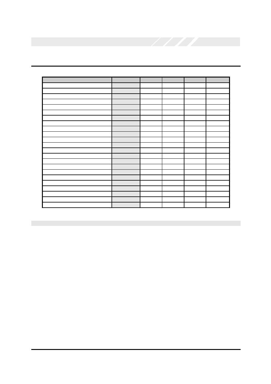
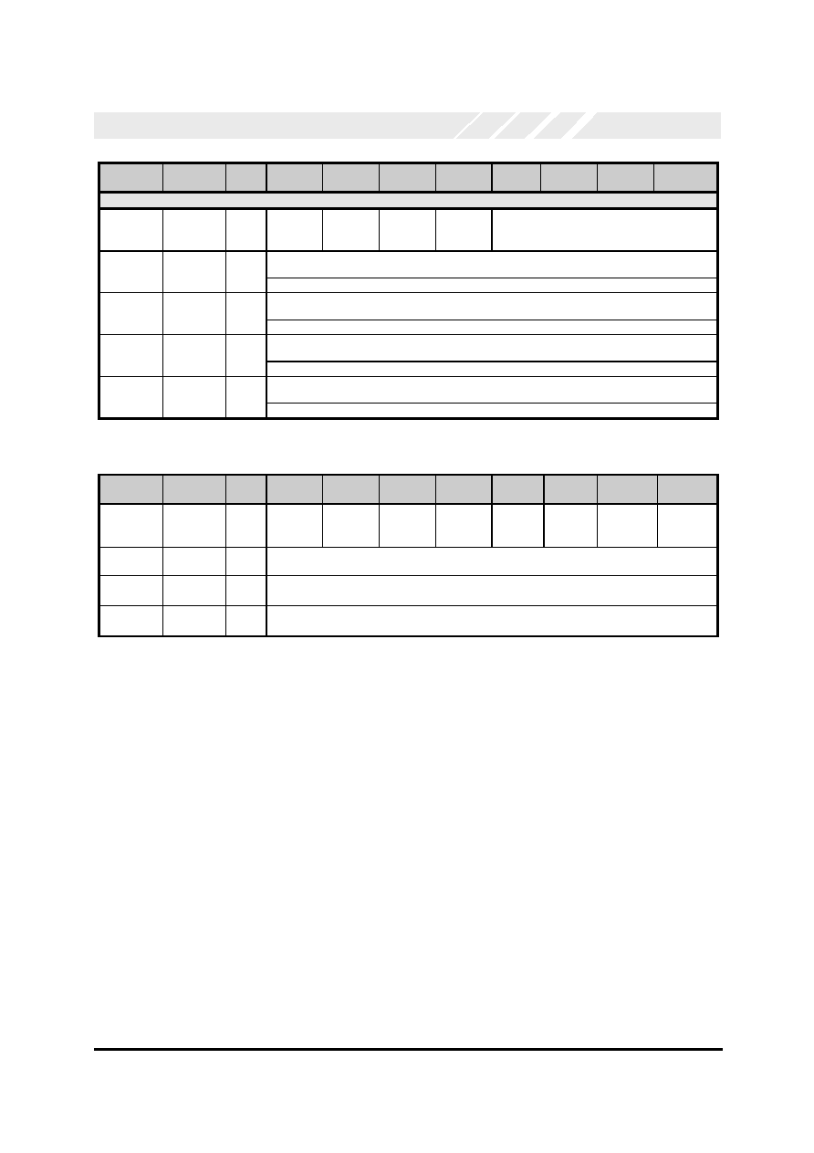
1
P
ERFORMANCE
C
OMPARISON
Feature
OX16C954
16C454
16C554
16C654
16C750
Integrated Serial channels
4
4
4
4
1
Good-Data status
Yes
No
No
No
No
External 1x baud rate clock
Yes
No
No
No
No
Max baud rate in normal mode
15 Mbps
115 kbps 115 kbps 1.5 Mbps
1 Mbps
Max baud rate in 1x clock mode
60 Mbps
n/a
n/a
n/a
n/a
FIFO depth
128
1
16
64
64
Sleep mode
Yes
No
No
Yes
Yes
Auto Xon/Xoff flow
Yes
No
No
Yes
No
Auto CTS#/RTS# flow
Yes
No
No
Yes
Yes
Auto DSR#/DTR# flow
Yes
No
No
No
No
No. of Rx interrupt thresholds
128
1
4
4
4
No. of Tx interrupt thresholds
128
1
1
4
1
No. of flow control thresholds
128
n/a
n/a
4
n/a
Transmitter empty interrupt
Yes
No
No
No
No
Readable status of flow control
Yes
n/a
No
No
No
Readable FIFO levels
Yes
n/a
No
No
No
Clock prescaler options
248
n/a
n/a
2
n/a
Rx/Tx disable
Yes
No
No
No
No
Software reset
Yes
No
No
No
No
Device ID
Yes
No
No
No
No
9-bit data frames
Yes
No
No
No
No
RS485 buffer enable
Yes
No
No
No
No
Infra-red (IrDA)
Yes
No
No
Yes
No
Table 1 OX16C954 performance compared with 16C454, 16C554, 16C654 and 16C750 devices
Improvements of the OX16C954 over previous generations of PC UARTs:
Deeper FIFOs:
The OX16C954 offers 128-byte deep FIFOs for the
transmitter and receiver.
Higher data rates:
Transmission and reception baud rates up to 15Mbps. A
flexible clock prescaler offers division ratios of 1 to 31 7/8
in steps of 1/8 using a divide-by-"M N/8" circuitry. The
flexible prescaler allows users to select from a wide variety
of input clock frequencies as well as access to higher baud
rates whilst maintaining compatibility with existing software
drivers (see section 14.2).
External clock option:
The receiver can accept an external clock on the DSR#
input. The transmitter can accept a 1x clock on the RI#
input and/or assert its own (Nx) clock on the DTR# output.
In 1x mode, asynchronous data may be transmitted and
received at speeds up to 60 Mbps (see section 14.6).
Automatic flow control:
The UART automatically handles either or both in-band
(software) flow control (transmitting and receiving Xon/Xoff
characters) and out-of-band (hardware) flow control using
the RTS#/CTS# or DSR#/DTR# modem control lines.
Special character detection:
The receiver can be programmed to generate an interrupt
upon reception of a particular character value.
Power-down:
The device can be placed in `sleep mode' to conserve
power
Readable FIFO levels:
Driver efficiency can be improved by using readable FIFO
levels.
Selectable trigger levels:
The receiver FIFO threshold can be arbitrarily
programmed. The transmitter FIFO threshold and

Data Sheet Revision 1.0 Page 6
OX16C954 rev B
OXFORD SEMICONDUCTOR LTD.
thresholds for automatic flow control can be programmed
to operate at a variety of trigger levels.
TX/RX Disable:
The transmitter and receiver can be independently
disabled.
Additional status:
Software drivers are able to read the status of in-band and
out-of-band automatic flow control, and distinguish
between XOFF and special character received interrupts.
Software reset:
The software driver may reset the device to recover from
unforeseen or unusual error conditions.
Transmitter empty interrupt:
The transmitter can generate an interrupt when the FIFO
and shift register are both empty.
RS485 buffer enable:
The function of the DTR# pin may be re-assigned to buffer-
enable signal for RS485 line driver in half-duplex mode
(see ACR[4:3] in section 15.3).
Device ID:
Four bytes of device ID are available to identify the
OX16C954 device to software drivers.
Infrared `IrDA' interface:
The UART contains an IrDA compliant modulator and
demodulator.
9-bit data framing
The UART may be configured for use in 9-bit character
framing for multi-drop protocols, where a tag ID (9
th
bit)
differentiates address and data characters.
Dual Voltage Operation(TQFP)
The 80pin TQFP package option can operate with supply
voltages of either 5.0v or 3.3v, thereby reducing inventory
controls. The VDETECT pin will need to be set according
to the voltage environment.
Data Sheet Revision 1.0 Page 7
OX16C954 rev B
OXFORD SEMICONDUCTOR LTD.
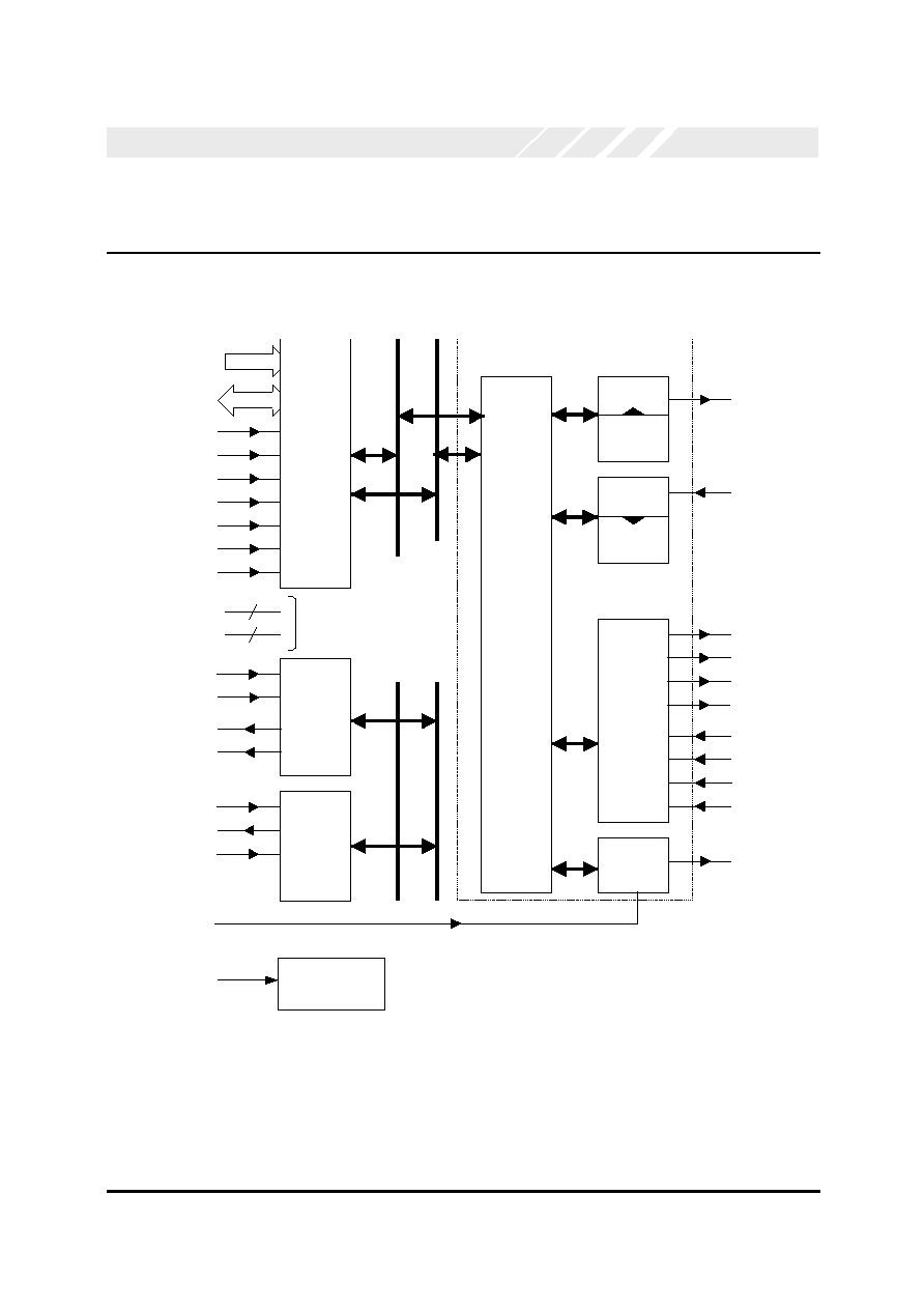
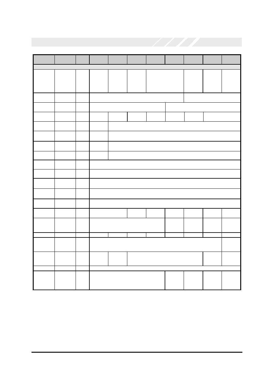
2
B
LOCK
D
IAGRAM
RESET / RESET#
Intel &
Motorola
Bus
Interface
A[2:0]
D[7:0]
CS0# / CS#
CS1# / A[3]
CS2# / A[4]
I/M#
IOR#
IOW# / R/W#
Control
and DMA
Interface
FIFOSEL
RXRDY#
TXRDY#
Modem
Control
Interface
RTSn#
DTRn#
OUT1n
OUT2n
CTSn#
DSRn#
DCDn#
RIn#
Clock &
Baud Rate
Generator
XTLI
XTLO
CLKSEL
Interrupt
Control
Logic
INTn
Receiver
SINn
Transmitter
SOUTn
128 Byte
FIFO
128 Byte
FIFO
Internal Data Bus
Internal Control Bus
Control
and
Status
Registers
VDD
GND
Power
supply
CS3#
2
4
SERIAL CHANNEL n ( 1 of 4 shown )
INTEN#
V D E T E C T *
5v / 3.3v
IO Buffer Control
Figure 1: OX16C954 Block Diagram
NOTE : VDETECT pin is only available on the 80pin TQFP package option
Data Sheet Revision 1.0 Page 8
OX16C954 rev B
OXFORD SEMICONDUCTOR LTD.
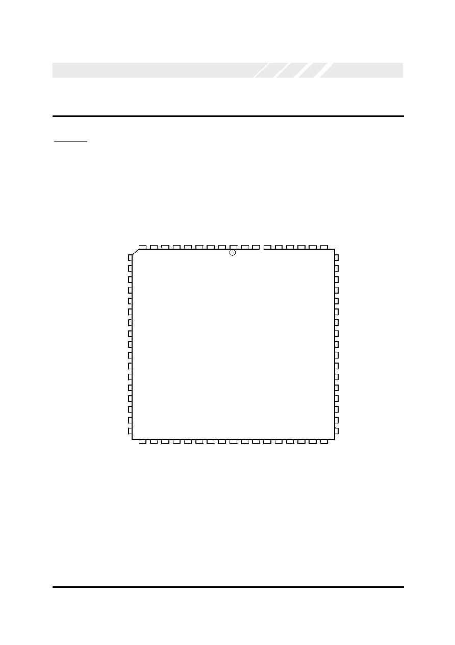
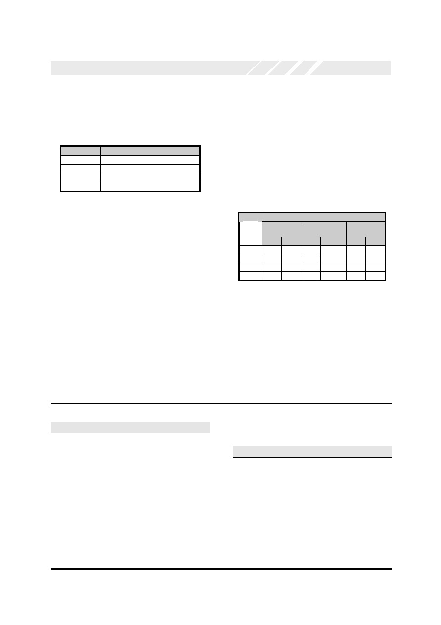
3 PIN INFORMATION
68pin PLCC
DC
D0
#
RI
0#
SI
N0
GN
D
DB
7
DB
6
DB
5
DB
4
DB
3
DB
2
DB
1
DB
0
IN
TS
EL
#
FIF
OS
EL
#
SI
N3
RI
3#
DC
D3
#
9
8
7
6
5
4
3
2
1
68
67
66
65
64
63
62
61
DSR0#
10
60
DSR3#
CTS0#
11
59
CTS3#
DTR0#
12
58
DTR3#
VDD
13
57
GND
RTS0#
14
56
RTS3#
INT0 / IRQ#
15
55
INT3
CS0# / DS#
16
54
CS3#
SOUT0
17
53
SOUT3
IOW # / R/W #
18
52
IOR#
SOUT1
19
51
SOUT2
CS1# / A3
20
50
CS2# / A4
INT1
21
49
INT2
RTS1#
22
48
RTS2#
GND
23
47
VDD
DTR1#
24
46
DTR2#
CTS1#
25
45
CTS2#
DSR1#
26
44
DSR2#
27
28
29
30
31
32
33
34
35
36
37
38
39
40
41
42
43
DC
D1
#
RI
1#
SI
N1
CL
KS
EL
I/M
#
A2
A1
A0
XT
LI
XT
LO
RE
SE
T /
RE
SE
T#
RX
RD
Y#
TX
RD
Y#
GN
D
SI
N2
RI
2#
DC
D2
#
OX16C954-PCC60-B
OX16C954-PCC60-B (Rev B) is pin compatible with the previous part OX16C954-PCC60-A (Rev A).
Data Sheet Revision 1.0 Page 9
OX16C954 rev B
OXFORD SEMICONDUCTOR LTD.
80pin TQFP
O X 1 6 C 9 5 4 _ T Q C 6 0 _ B
2
3
4
5
1
7
8
9
1 0
6
1 2
1 3
1 4
1 5
1 1
1 7
1 8
1 9
2 0
1 6
5 9
5 8
5 7
5 6
6 0
5 4
5 3
5 2
5 1
5 5
4 9
4 8
4 7
4 6
5 0
4 4
4 3
4 2
4 1
4 5
2 1
2 5
2 4
2 2 2 3
3 0
2 9
2 6 2 7 2 8
3 1
3 5
3 4
3 2 3 3
4 0
3 9
3 6 3 7 3 8
7 6
7 7
7 9 7 8
7 1
7 2
7 5 7 4 7 3
7 0
6 6
6 7
6 9 6 8
6 1
6 2
6 5 6 4 6 3
8 0
T X R D Y 3 #
D C D 3 #
RI3#
S I N 3
F I F O S E L #
I N T S E L #
D B 0
D B 1
D B 2
N C
D B 3
D B 4
D B 5
D B 6
D B 7
G N D
S I N 0
RI0#
D C D 0 #
R X R D Y 0 #
R X R D Y 2 #
D C D 2 #
RI2#
S I N 2
G N D
T X R D Y #
R X R D Y #
R E S E T / R E S E T #
V D E T E C T
X T L O
XTLI
I/M#
A 0
A 1
A 2
C L K S E L
S I N 1
RI1#
D C D 1 #
T X R D Y 1 #
RTS2#
RXRDY3#
DSR3#
CTS3#
DTR3#
GND
SOUT3
CS3#
INT3
NC
IOR#
SOUT2
CS2# / A4
VDD
DTR2#
CTS2#
TXRDY2#
DSR2#
TXRDY0#
DSR0#
CTS0#
DTR0#
VDD
RTS0#
INT0 / IRQ#
NC
SOUT0
CS0# / DS#
IOW# / R/R#
SOUT1
CS1# / A3
INT1
RTS1#
GND
DTR1#
RXRDY1#
DSR1#
CTS1#
INT2
Z_RTS3
Data Sheet Revision 1.0 Page 10
OX16C954 rev B
OXFORD SEMICONDUCTOR LTD.
4 P
IN
D
ESCRIPTIONS
Please refer to Section 3 for actual Signal Name to Pin Number assignments, for the selected package.
TQFP
PLCC
Dir
1
Name
Description
Clock
50
35
I
XTLI
Crystal oscillator input or external clock pin, for the UART channels.
Crystal oscillator frequency maximum 60MHz
51
36
O
XTLO
Crystal oscillator output.
Not used when an alternative TTL level clock is applied to XTLI and can
be left unconnected
45
30
I
CLKSEL
This pin is provided to select an internal clock prescaler on power up. In
16C554 devices this pin is a VDD. When CLKSEL pin is high the internal
prescaler is bypassed (a 1.8432MHz clock is assumed). Connect this pin
to GND to enable the internal clock prescaler. The complement of this pin
is loaded in bit 7 of the MCR register after a hardware reset.
This pin can also be used as an alternative external clock pin under
software control (replacing XTLI and thus reducing noise/power due to
XTLO) for embedded applications.
Processor Interface Pins in Intel Mode (I/M# = `1')
53
37
I
RESET
Active-high Hardware Reset. The configuration of OX16C954 after a
hardware reset is described in section 7.1. This pin exhibits a small
hysteresis to provide noise immunity. This pin must be tied inactive when
not in use.
73
68
33
28
54
50
20
16
I
I
I
I
CS[3]#
CS[2]#
CS[1]#
CS[0]#
Active-low Chip-Selects for each Uart channel, in Intel bus mode.
CS3# - Chip select for Uart 3
CS2# - Chip select for Uart 2
CS1# - Chip select for Uart 1
CS0# - Chip select for Uart 0
46 to 48 32 to 34 I
A[2:0]
Address lines to select the Uart (channel) registers.
15 to 11
9 to 7
5 to 1
68 to 66
I/O
DB[7:0]
Eight-bit 3-state data bus.
31
18
I
IOW#
Active-low write strobe in Intel bus mode.
70
52
I
IOR#
Active-low read strobe in Intel bus mode.
Processor Interface Pins in Motorola Mode (I/M# = `0')
53
37
I
RESET#
Active-low Hardware Reset. The configuration of OX16C954 after a
hardware reset is described in section 7.1. This pin exhibits a small
hysteresis to provide noise immunity. This pin must be tied inactive when
not in use.
28
16
I
DS#
Active-low Data-Strobe.
(In Motorola bus mode, individual registers are accessed using DS#,
R/W# and A[4:0])
70
73
52
54
I
I
UNUSED
In Motorola bus mode these pins are unused and must be connected to
VDD or GND.
68
33
50
20
I
I
A4
A3
The A[4:3] combination selects individual channels as follows:
00 = UART 0 selected
01 = UART 1 selected
10 = UART 2 selected
11 = UART 3 selected
46 to 48 32 to 34 I
A[2:0]
Address lines to select the UART (channel) registers.

Data Sheet Revision 1.0 Page 11
OX16C954 rev B
OXFORD SEMICONDUCTOR LTD.
TQFP
PLCC
Dir
1
Name
Description
Processor Interface Pins in Motorola Mode (I/M# = `0') Contd.
15 to 11
9 to 7
5 to 1
68 to 66
I/O
DB[7:0]
Eight-bit 3-state data bus.
31
18
I
R/W#
Read-not-write signal. This signal should be high during read cycles and
low during write cycles.
Serial Port Pins
72
69
32
29
72
69
32
29
53
51
19
17
53
51
19
17
O
O
O
O
O
O
O
O
SOUT[3]
SOUT[2]
SOUT[1]
SOUT[0]
IrDA_Out[3]
IrDA_Out[2]
IrDA_Out[1]
IrDA_Out[0]
Serial data output, Uart 3
Serial data output, Uart 2
Serial data output, Uart 1
Serial data output, Uart 0
UART IrDA data outputs, each Uart, respectively.
Serial data output pins are redefined as IrDA data outputs when MCR[6]
of the corresponding UART channel is set in enhanced mode
75
66
35
26
56
48
22
14
O
O
O
O
RTS[3]#
RTS[2]#
RTS[1]#
RTS[0]#
Active-low Request-To-Send output, for each uart respectively.
Whenever the automated RTS# flow control is enabled for the
corresponding channel, the RTS# pin is de-asserted and re-asserted if the
receiver FIFO reaches or falls below a pair of programmed flow control
thresholds, respectively. The state is controlled by bit 1 of the MCR.
RTS may also be used as a general-purpose output.
77
64
37
24
77
64
37
24
77
64
37
24
58
46
24
12
58
46
24
12
58
46
24
12
O
O
O
O
O
O
O
O
O
O
O
O
DTR[3]#
DTR[2]#
DTR[1]#
DTR[0]#
485_En[3]
485_En[2]
485_En[1]
485_En[0]
TxClkOut[3]
TxClkOut[2]
TxClkOut[1]
TxClkOut[0]
Active-low modem "data-terminal-ready output", for each uart respectively.
If automated DTR# flow control is enabled for the corresponding UART
channel, the DTR# pin is asserted and deasserted if the receiver FIFO
reaches or falls below the channel's programmed thresholds, respectively.
The state is set by bit 0 of the MCR. DTR may also be used as a general
purpose output
.
In RS485 half-duplex mode, the DTR# pin of each UART channel may be
programmed to reflect the state of the channel's transmitter empty bit (or
its inverse) to automatically control the direction of the RS485 transceiver
buffer (see register ACR[4:3])
Transmitter 1x (or baud rate generator output) clock. For isochronous
applications, the 1x (or Nx) transmitter clock may be asserted on the
uart's DTR# pin (see CKS[5:4]).
4
57
44
17
4
57
44
17
63
41
29
7
63
41
29
7
I
I
I
I
I
I
I
I
SIN[3]
SIN[2]
SIN[1]
SIN[0]
IrDA_In[0:3]
IrDA_In[0:3]
IrDA_In[0:3]
IrDA_In[0:3]
Serial data input, UART 3.
Serial data input, UART 2.
Serial data input, UART 1.
Serial data input, UART 0.
UART IrDA data inputs, for each uart respectively.
Serial data input pins redefined as IrDA data inputs when MCR[6] of the
corresponding UART channel is set in enhanced mode
78
63
38
23
59
45
25
11
I
I
I
I
CTS[3]#
CTS[2]#
CTS[1]#
CTS[0]#
Active-low modem "clear-to-send" input, for each uart respectively.
If automated CTS# flow control is enabled for the corresponding UART
channel, upon deassertion of the CTS# pin, the channel's transmitter will
complete the current character and enter the idle mode until the CTS# pin
is reasserted. Note: flow control characters are transmitted regardless of
the state of the CTS# pin. The state of this pin is reflected in bit 4 of the
MSR.
It can also be used as a general-purpose input
.

Data Sheet Revision 1.0 Page 12
OX16C954 rev B
OXFORD SEMICONDUCTOR LTD.
TQFP
PLCC
Dir
1
Name
Description
Serial Port Pins Contd.
79
62
39
22
79
62
39
22
60
44
26
10
60
44
26
10
I
I
I
I
I
I
I
I
DSR[3]#
DSR[2]#
DSR[1]#
DSR[0]#
RxClkIn[3]
RxClkIn[2]
RxClkIn[1]
RxClkIn[0]
Active-low modem "data-set-ready" input, for each uart respectively.
If automated DSR# flow control is enabled for the corresponding UART
channel, upon deassertion of the channel's DSR# pin, the transmitter will
complete the current character and enter the idle mode until the DSR# pin
is reasserted. Note: flow control characters are transmitted regardless of
the state of the DSR# pin. The state of this pin is reflected in bit 5 of the
MSR.
It can also be used as a general-purpose input
.
External receiver clock for isochronous applications for each uart
respectively. Selected when CKS[1:0] = `01'.
2
59
42
19
61
43
27
9
I
I
I
I
DCD[3]#
DCD[2]#
DCD[1]#
DCD[0]#
Active-low modem Data-Carrier-Detect input, for each uart respectively.
The state of this pin is reflected in bit 7 of the MSR. It can also be used
as a general-purpose input
.
3
58
43
18
3
58
43
18
62
42
28
8
62
42
28
8
I
I
I
I
I
I
I
I
RI[3]#
RI[2]#
RI[1]#
RI[0]#
Ext_CK[3]
Ext_CK[2]
Ext_CK[1]
Ext_CK[0]
Active-low modem Ring-Indicator input, for each uart respectively.
The state of this pin is reflected in bit 6 of the MSR. It can also be used
as a general-purpose input
. RI can be configured as tx and rx for a 1x
clock in isochronous operation.
External transmitter clock for each uart respectively. This clock can be
used by the transmitter (and by the receiver indirectly) when CKS[6] = `1'.
Interrupt & DMA Pins
1
61
41
21
No pin
No pin
No pin
No pin
O
O
O
O
TXRDY3#
TXRDY2#
TXRDY1#
TXRDY0#
Signal for the DMA transfer of transmitter data, for Uart 3.
Signal for the DMA transfer of transmitter data, for Uart 2.
Signal for the DMA transfer of transmitter data, for Uart 1.
Signal for the DMA transfer of transmitter data, for Uart 0.
There are two modes of DMA signalling described in section 8.1
55
39
O
TXRDY#
Signal for the DMA transfer of transmitter data.
This pin is the wire "OR-ed" function of the TXRDY# signals of all
channels.
80
60
40
20
No pin
No pin
No pin
No pin
O
O
O
O
RXRDY3#
RXRDY2#
RXRDY1#
RXRDY0#
Signal for the DMA transfer of receiver data, for Uart 3.
Signal for the DMA transfer of receiver data, for Uart 2.
Signal for the DMA transfer of receiver data, for Uart 1.
Signal for the DMA transfer of receiver data, for Uart 0.
There are two modes of DMA signalling described in section 8.1
54
38
O
RXRDY#
Signal for DMA transfer of received data.
This pin is the wire "OR-ed" function of the RXRDY# signals of all
channels.

Data Sheet Revision 1.0 Page 13
OX16C954 rev B
OXFORD SEMICONDUCTOR LTD.
TQFP
PLCC
Dir
1
Name
Description
Interrupt & DMA Pins Contd.
74
67
34
55
49
21
O
O
O
INT[3]
INT[2]
INT[1]
Interrupt pin for Uart channel 3 (Intel Bus mode)
Interrupt pin for Uart channel 2 (Intel Bus mode)
Interrupt pin for Uart channel 1 (Intel Bus mode)
Each of these serial channels have a 3-state interrupt output (enabled by
MCR[3] and INTSEL# pin) which goes active (high) when an interrupt
condition occurs. The interrupt is disabled after a hardware reset.
27
27
15
15
O
OD
INT0
IRQ#
Interrupt pin for Uart channel 0, in Intel bus mode.
This serial channel has a 3-state interrupt output (enabled by MCR[3] and
INTSEL# pin) which goes active (high) when an interrupt condition occurs.
The interrupt is disabled after a hardware reset.
Device interrupt pin (for all uart channels) in Motorola bus mode.
This pin goes active (low) when the interrupt signal from any of the 4
channels is asserted. Otherwise it is in the high-impedance state.
Miscellaneous Pins
6
65
ID
INTSEL#
Active-low Interrupt enable.
When this pin is left open or connected to GND, the three-state interrupts
that are available on INT[3:0] are enabled according to the setting of
MCR[3]. If this pin is high interrupts are enabled regardless of the state of
MCR[3].
This pin is ignored in Motorola bus mode.
49
31
IU
I/M#
Intel or Motorola bus interface select.
When this pin is tied high or left open, the Intel bus interface is selected.
When this pin is tied low, the Motorola bus interface is selected where
RESET, IOW#, CS0#, CS1# are CS2# are re-assigned and CS3#, IOR#
and INTSEL# are unused. In Motorola mode, all the interrupt lines of the
internal uart channels are wired "OR-ed" onto the IRQ# pin.
In 16C554 this pin is unconnected
.
5
64
I
FIFOSEL#
FIFO SIZE select.
For backward compatibility with 16C554, 16C654 and 16C754 devices the
FIFO depth is 16 when FIFOSEL# is high and 128 when FIFOSEL# is
low. The unlatched state of this pin is readable by software. The FIFO size
may be set to 128 by writing a 1 in FCR[5] when LCR[7] is set or by
putting the device into Enhanced mode, thus overriding the state of the
FIFOSEL# pin. Pin 64 is a VDD in 16C554 and 16C654 devices (PLCC).
52
No pin
ID
VDETECT
3.3v or 5.0v I/O buffer selection.
This pin must be tied according to the voltage supply used to power the
TQFP package option.
For 5v supply voltage : Vdetect must be tied low.
For 3.3v supply voltage : Vdetect must be tied high.
NOTE : The PLCC package option does not bond-out this pin, which is
internally pulled down to gnd. So the PLCC is suitable for 5v operation
only
.

Data Sheet Revision 1.0 Page 14
OX16C954 rev B
OXFORD SEMICONDUCTOR LTD.
TQFP
PLCC
Dir
1
Name
Description
Power, Ground, No Connects
16, 36,
56, 76
6, 23,
40, 57
GND
Ground pin.
All GND pins must be tied to ground.
25, 65
13, 47
VDD
Power pin.
PLCC : All VDD pins must be tied to 5 Volts.
TQFP : All VDD pins must be tied to 5v or 3.3v. (Note that the VDETECT
pin must be set according to the selected voltage environment).
10, 30,
71
-
NC
No Connects
These pins are not connected to any pads within the device, and can be
left open.
Table 2: Pin Descriptions
Direction key:
I, Input
IU Input with pull-up
ID Input with pull-down
O Output
I/O Bi-directional
OD Open drain
Note: All unused signal input pins should be tied to VDD or GND as applicable and must not be left floating. For high speed operation (XTAL >
10MHz), card designers are recommended to follow the guidelines for high-speed digital design such as maintaining PCB tracks as short
as possible, using a multi-layer PCB with separate power and ground planes, and using good-quality de-coupling capacitors.
Attention should be given to high frequency decoupling of power and ground pins due to the high frequency internal switching that occurs
under normal operation
Data Sheet Revision 1.0 Page 15
OX16C954 rev B
OXFORD SEMICONDUCTOR LTD.
4.1 Further Pin Information
Pin
Description
Action when used
Action when not used
Intel TM Mode Bus Interface Pins
I/M#
Intel / Motorola Mode Tie high for IntelTM style bus mode
Leave unconnected (Internal pull-up)
CS0#-CS3#
Chip selects
Connect direct to active low channel select
signals for UART channels 0-3 respectively
n/a
MotorolaTM Mode Bus Interface Pins
I/M#
Intel / Motorola Mode Tie low for Motorola TM style bus mode
n/a
Must be tied low for Motorola mode
DS# (CS0#)
Data Strobe
Connect direct to data strobe generator logic
n/a
A3-4 (CS1-2#)
Additional address
lines
Connect direct to channel selection logic
A[4:3] = 00 = ch. 1, 01 = ch. 2 etc.
n/a
IRQ# (INT0)
Global interrupt
Interrupt for all channels. Connect to an
available processor interrupt line
Leave unconnected
(Interrupts can not be used)
CS3#
Unused
n/a
Tie high
INT1-3
Unused
n/a
Leave unconnected
Control Pins
INTSEL
Interrupt Control
Mode (used in Intel
mode only)
Tie high to keep the interrupt pins
permanently enabled.
Tie low or leave unconnected to allow
software enable/disable of the
interrupt pin.
DMA Pins
RXRDY#
DMA Control signal
output
Connect direct to DMA control circuitry
Leave unconnected
TXRDY#
DMA Control signal
output
Connect direct to DMA control circuitry
Leave unconnected
Common Channel Pins
SOUT
Serial data output
Connect to a suitable line driver
Leave unconnected
(Serial data can not be transmitted)
SIN
Serial data input
Connect to a suitable line receiver
Leave unconnected
(Serial data can not be received)
RTS#
Request-To-Send
Modem signal output
Connect to a suitable line driver
Leave unconnected
CTS#
Clear-To-Send
Modem signal input
Connect to a suitable line receiver
Tie high
DTR#
Data-Terminal-Ready
Modem signal output
Connect to a suitable line driver
Leave unconnected
DSR#
Data-Set-Ready
Modem signal input
Connect to a suitable line receiver
Tie high
DCD#
Data-Carrier-Detect
Modem signal input
Connect to a suitable line receiver
Tie high
RI#
Ring-Indicator
Modem signal input
Connect to a suitable line receiver
Tie high
INT
Interrupt Output
Connect to an available processor interrupt
line
Leave unconnected
(Interrupts can not be used)
Data Sheet Revision 1.0 Page 16
OX16C954 rev B
OXFORD SEMICONDUCTOR LTD.
5 M
ODE
S
ELECTION
The OX16C954 device is a four-channel device backward compatible with the 16C454, 16C554, 16C654 and 16C750 UARTs.
Each of the four channels are identical and independent in terms of functionality, with the exception of some shared pins (for
example, CLKSEL, FIFOSEL#, CLK and RESET). The remainder of this document therefore discusses the operation of a single
channel only.
The operation of each Uart Channel depends on a number of mode settings, which are referred to throughout this section. The
modes, conditions and corresponding FIFO depth are tabulated below:
UART Mode
FIFO
size
FCR[0] Enhanced mode
(EFR[4]=1)
FCR[5]
(guarded with LCR[7] = 1)
FIFOSEL#
Pin
450
1
0
X
X
X
550
16
1
0
0
1
Extended 550
128
1
0
X
0
650
128
1
1
X
X
750
128
1
0
1
1
950
1
128
1
1
X
X
Table 3: UART Mode Configuration
Note 1: 950 mode configuration is identical to 650 configuration
5.1 450 Mode
After a hardware reset, bit 0 of the FIFO Control Register
(`FCR') is cleared, hence the UART is compatible with the
16C450. The transmitter and receiver FIFOs (referred to as
the `Transmit Holding Register' and `Receiver Holding
Register' respectively) have a depth of one. This is referred
to as `Byte mode'. When FCR[0] is cleared, all other mode
selection parameters are ignored.
5.2 550 Mode
Connect FIFOSEL# to VDD. After a hardware reset, writing
a 1 to FCR[0] will increase the FIFO size to 16, providing
compatibility with 16C550 devices. Since this pin is VDD in
16C554 devices, replacing a 16C554 with OX16C954
would result in a 550 compatible device with 16 byte deep
FIFOs.
5.3 Extended 550 Mode
Connect FIFOSEL# to GND. Writing a 1 to FCR[0] will now
increase the FIFO size to 128, thus providing a 550 device
with 128 deep FIFOs.
5.4 750 Mode
Writing a 1 to FCR[0] will increase the FIFO size to 16. In a
similar fashion to 16C750, the FIFO size can be further
increased to 128 by writing a 1 to FCR[5]. Note that access
to FCR[5] is protected by LCR[7]. i.e., to set FCR[5],
software should first set LCR[7] to temporarily remove the
guard. Once FCR[5] is set, the software should clear
LCR[7] for normal operation.
The 16C750 additional features are available as long as
the UART is not put into Enhanced mode; i.e. ensure
EFR[4] = `0'. These features are:
·
Deeper FIFOs
·
Automatic RTS/CTS out-of-band flow control
·
Sleep mode
5.5 650 Mode
The OX16C954 UART is compatible with the 16C650 when
EFR[4] is set, i.e. the device is in Enhanced mode. As 650
software drivers usually put the device in Enhanced mode,
running 650 drivers on the one of the UART channels will
result in 650 compatibility with 128 deep FIFOs, as long as
FCR[0] is set. Note that the 650 emulation mode of the
OX16C954 provides 128-deep FIFOs whereas the
standard 16C650 has only 32 byte FIFOs.
650 mode has the same enhancements as the 16C750
over the 16C550, but these are enabled using different
registers.
There are also additional enhancements over those of the
16C750 in this mode. These are -
1. Automatic in-band flow control
2. Special character detection

Data Sheet Revision 1.0 Page 17
OX16C954 rev B
OXFORD SEMICONDUCTOR LTD.
3. Infra-red "IrDA-format" transmit and receive mode
4. Transmit trigger levels
5. Optional clock prescaler
5.6 950 Mode
The additional features offered in 950 mode generally only
apply when the UART is in Enhanced mode (EFR[4]='1').
Provided FCR[0] is set, in Enhanced mode the FIFO size is
128 regardless of the state of FIFOSEL#.
Note that 950 mode configuration is identical to that of 650
mode, however additional 950 specific features are
enabled using the Additional Control Register `ACR' (see
section 15.3). In addition to larger FIFOs and higher baud
rates, the enhancements of the 950 mode over 650
emulation mode are:
·
Selectable arbitrary trigger levels for the receiver and
transmitter FIFO interrupts
·
Improved automatic flow control using selectable
arbitrary thresholds
·
DSR#/DTR# automatic flow control
·
Transmitter and receiver can be optionally disabled
·
Software reset of device
·
Readable FIFO fill levels
·
Optional generation of an RS-485 buffer enable signal
·
Four-byte device identification (0x16C95404)
·
Readable status for automatic in-band and out-of-
band flow control
·
External 1x clock modes (see section14.4)
·
Flexible "M+N/8" clock prescaler (see section 14.2)
·
Programmable sample clock to allow data rates up to
15 Mbps (see section 14.3).
·
9-bit data mode
The 950 trigger levels are enabled when ACR[5] is set (bits
4 to 7 of FCR are ignored). Then arbitrary trigger levels can
be defined in RTL, TTL, FCL and FCH registers (see
section 15). The Additional Status Register (`ASR') offers
flow control status for the local and remote transmitters.
FIFO levels are readable using RFL and TFL registers.
The UART has a flexible prescaler capable of dividing the
system clock by any value between 1 and 31.875 in steps
of 0.125. It divides the system clock by an arbitrary value in
"M+N/8" format, where M and N are 5- and 3-bit binary
numbers programmed in CPR[7:3] and CPR[2:0]
respectively. This arrangement offers a great deal of
flexibility when choosing an input clock frequency to
synthesise arbitrary baud rates. The default division value
is 4 to provide backward compatibility with 16C650
devices.
The user may apply an external 1x (or Nx) clock for the
transmitter and receiver to the RI# and DSR# pin
respectively. The transmitter clock may instead be asserted
on the DTR# pin. The external clock options are selected
through the CKS register (offset 0x02 of ICR).
It is also possible to define the over-sampling rate used by
the transmitter and receiver clocks. The 16C450/16C550
and compatible devices employ 16 times over-sampling,
where there are 16 clock cycles per bit. However the 950
UART can employ any over-sampling rate from 4 to 16 by
programming the TCR register. This allows the data rates
to be increased to 460.8 Kbps using a 1.8432MHz clock, or
15 Mbps using a 60 MHz clock. The default value after a
reset for this register is 0x00, which corresponds to a 16
cycle sampling clock. Writing 0x01, 0x02 or 0x03 will also
result in a 16 cycle sampling clock. To program the value to
any value from 4 to 15 it is necessary to write this value
into the TCR i.e. to set the device to a 13 cycle sampling
clock it would be necessary to write 0x0D to TCR. For
further information see section 14.3.
The UART also offers 9-bit data frames for multi-drop
industrial applications.
Data Sheet Revision 1.0 Page 18
OX16C954 rev B
OXFORD SEMICONDUCTOR LTD.
6 R
EGISTER DESCRIPTION TABLES
The UART is accessed through an 8-byte block of I/O space (or through memory space). Since there are more than 8 registers,
the mapping is also dependent on the state of the Line Control Register `LCR' and Additional Control Register `ACR':
1. LCR[7]=1 enables the divider latch registers DLL and DLM.
2. LCR specifies the data format used for both transmitter and receiver. Writing 0xBF (an unused format) to LCR enables
access to the 650 compatible register set. Writing this value will set LCR[7] but leaves LCR[6:0] unchanged. Therefore, the
data format of the transmitter and receiver data is not affected. Write the desired LCR value to exit from this selection.
3. ACR[7]=1 enables access to the 950 specific registers.
4. ACR[6]=1 enables access to the Indexed Control Register set (ICR) registers as described on page 20.
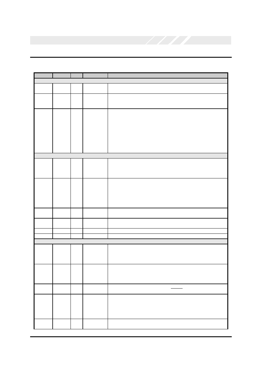
Register
Name
Address R/W
Bit 7
Bit 6
Bit 5
Bit 4
Bit 3
Bit 2
Bit 1
Bit 0
THR
1
000
W
Data to be transmitted
RHR
1
000
R
Data received
IER
1,2
650/950
Mode
CTS
interrupt
mask
RTS
interrupt
mask
Special
Char.
Detect
550/750
Mode
001
R/W
Unused
Alternate
sleep
mode
Sleep
mode
Modem
interrupt
mask
Rx Stat
interrupt
mask
THRE
interrupt
mask
RxRDY
interrupt
mask
FCR
3
650 mode
RHR Trigger
Level
THR Trigger
Level
750 mode
RHR Trigger
Level
FIFO
Size
Unused
950 mode
010
W
Unused
DMA
Mode /
Tx
Trigger
Enable
Flush
THR
Flush
RHR
Enable
FIFO
ISR
3
010
R
FIFOs
enabled
Interrupt priority
(Enhanced mode)
Interrupt priority
(All modes)
Interrupt
pending
LCR
4
011
R/W
Divisor
latch
access
Tx
break
Force
parity
Odd /
even
parity
Parity
enable
Number
of stop
bits
Data length
MCR
3,4
550/750
Mode
Unused
CTS &
RTS
Flow
Control
650/950
Mode
100
R/W
Baud
prescale
IrDA
mode
XON-Any
Enable
Internal
Loop
Back
OUT2
(interrupt
enable)
OUT1
(not
used)
RTS
DTR
LSR
3,5
Normal
Data
Error
Tx Empty
THR
Empty
Rx
Break
Framing
Error
Parity
Error
Overrun
Error
RxRDY
9-bit data
mode
101
R
9
th
Rx
data bit
MSR
3
110
R
DCD
RI
DSR
CTS
Delta
DCD
Trailing
RI edge
Delta
DSR
Delta
CTS
SPR
3
Normal
Temporary data storage register and
Indexed control register offset value bits
9-bit data
mode
111
R/W
Unused
9
th
Tx
data bit
Additional Standard Registers These registers require divisor latch access bit (LCR[7]) to be set to 1.
DLL
000
R/W
Divisor latch bits [7:0] (Least significant byte)
DLM
001
R/W
Divisor latch bits [15:8] (Most significant byte)
Table 4: Standard 550 Compatible Registers
Data Sheet Revision 1.0 Page 19
OX16C954 rev B
OXFORD SEMICONDUCTOR LTD.
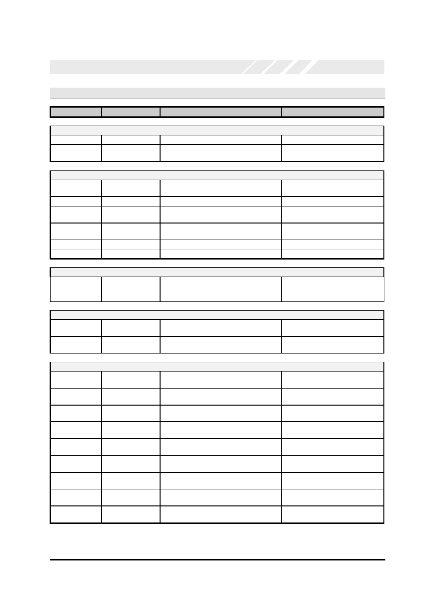
Register
Name
Address R/W
Bit 7
Bit 6
Bit 5
Bit 4
Bit 3
Bit 2
Bit 1
Bit 0
To access these registers LCR must be set to 0xBF
EFR
010
R/W
CTS
flow
control
RTS
Flow
control
Special
char
detect
Enhance
mode
In-band flow control mode
XON1
100
R/W
XON Character 1
9-bit mode
Special character 1
XON2
101
R/W
XON Character 2
9-bit mode
Special Character 2
XOFF1
110
R/W
XOFF Character 1
9-bit mode
Special character 3
XOFF2
111
R/W
XOFF Character 2
9-bit mode
Special character 4
Table 5: 650 Compatible Registers
Register
Name
Address R/W
Bit 7
Bit 6
Bit 5
Bit 4
Bit 3
Bit 2
Bit 1
Bit 0
ASR
1,6,7
001
R/W
7
Tx
Idle
FIFO
size
FIFO-
SEL
Special
Char
Detect
DTR
RTS
Remote
Tx
Disabled
Tx
Disabled
RFL
6
011
R
Number of characters in the receiver FIFO
TFL
3,6
100
R
Number of characters in the transmitter FIFO
ICR
3,8,9
101
R/W
Data read/written depends on the value written to the SPR prior to
the access of this register (see
Table 7
)
Table 6: 950 Specific Registers
Register access notes:
Note 1: Requires LCR[7] = 0
Note 2: Requires ACR[7] = 0
Note 3: Requires that last value written to LCR was not 0xBF
Note 4: To read this register ACR[7] must be = 0
Note 5: To read this register ACR[6] must be = 0
Note 6: Requires ACR[7] = 1
Note 7: Only bits 0 and 1 of this register can be written
Note 8: To read this register ACR[6] must be = 1
Note 9: This register acts as a window through which to read and write registers in the Indexed Control Register set
Data Sheet Revision 1.0 Page 20
OX16C954 rev B
OXFORD SEMICONDUCTOR LTD.
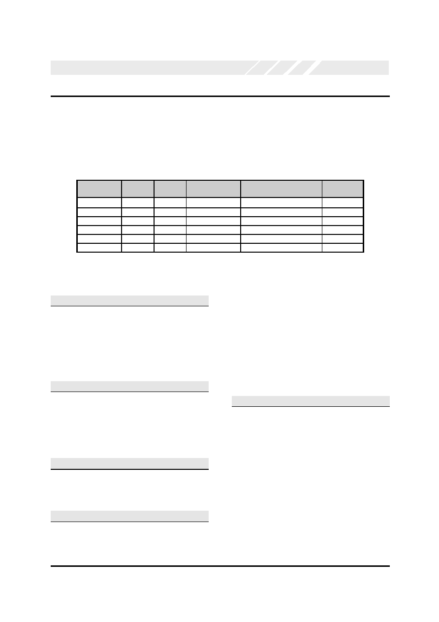
Register
Name
SPR
Offset
10
R/W
Bit 7
Bit 6
Bit 5
Bit 4
Bit 3
Bit 2
Bit 1
Bit 0
Indexed Control Register Set
ACR
0x00
R/W
Addit-
ional
Status
Enable
ICR
Read
Enable
950
Trigger
Level
Enable
DTR definition and
control
Auto
DSR
Flow
Control
Enable
Tx
Disable
Rx
Disable
CPR
0x01
R/W
5 Bit "integer" part of
clock prescaler
3 Bit "fractional" part of
clock prescaler
TCR
0x02
R/W
Unused
4 Bit N-times clock
selection bits [3:0]
CKS
0x03
R/W
Tx 1x
Mode
Tx CLK
Select
BDOUT
on DTR
DTR 1x
Tx CLK
Rx 1x
Mode
Unused
Receiver
Clock Sel[1:0]
TTL
0x04
R/W
Unused
Transmitter Interrupt Trigger Level (0-127)
RTL
0x05
R/W
Unused
Receiver Interrupt Trigger Level (1-127)
FCL
0x06
R/W
Unused
Automatic Flow Control Lower Trigger Level (0-127)
FCH
0x07
R/W
Unused
Automatic Flow Control Higher Trigger level (1-127)
ID1
0x08
R
Hardwired ID byte 1 (0x16)
ID2
0x09
R
Hardwired ID byte 1 (0xC9)
ID3
0x0A
R
Hardwired ID byte 1 (0x54)
REV
0x0B
R
Hardwired revision byte (0x04)
CSR
0x0C
W
Writing 0x00 to this register will
reset the UART (Except the CKS and CKA registers)
NMR
0x0D
R/W
Unused
9
th
Bit
SChar 4
9
th
Bit
SChar 3
9
th
Bit
SChar 2
9
th
Bit
SChar 1
9
th
-bit Int.
En.
9 Bit
Enable
MDM
0x0E
R/W
Reserved
DCD
Wakeup
disable
Trailing
RI edge
disable
DSR
Wakeup
disable
CTS
Wakeup
disable
RFC
0X0F
R
FCR[7]
FCR[6]
FCR[5]
FCR[4]
FCR[3]
FCR[2]
FCR[1]
FCR[0]
GDS
0X10
R
Unused
Good
Data
Status
DMS
0x11
R/W
Force
TxRdy
inactive
Force
RxRdy
inactive
Unused
TxRdy
status
( R )
RxRdy
status
( R )
PIDX
0x12
R
Hardwired Port Index ( 0x00, 0x01, 0x02, 0x03 respectively )
CKA
0x13
R/W
Unused
Use
CLKSEL
pin for
sys-clk
Invert
DTR
signal
Invert
internal
tx clock
Invert
internal
rx clock
Table 7: Indexed Control Register Set
Note 10: The SPR offset column indicates the value that must be written into SPR prior to reading / writing any of the Indexed Control Registers via ICR.
Offset values not listed in the table are reserved for future use and must not be used.

Data Sheet Revision 1.0 Page 21
OX16C954 rev B
OXFORD SEMICONDUCTOR LTD.
To read or write to any of the Indexed Controlled Registers use the following procedure:
Writing to ICR registers:
Ensure that the last value written to LCR was not 0xBF (reserved for 650 compatible register access value).
Write the desired offset to SPR (address 111b).
Write the desired value to ICR (address 101b).
Reading from ICR registers:
Ensure that the last value written to LCR was not 0xBF (see above).
Write 0x00 offset to SPR to select ACR.
Set bit 6 of ACR (ICR read enable) by writing x1xxxxxxb to address 101b. Ensure that other bits in ACR are not changed.
(Software drivers should keep a copy of the contents of the ACR elsewhere since reading ICR involves overwriting ACR!)
Write the desired offset to SPR (address 111b).
Read the desired value from ICR (address 101b).
Write 0x00 offset to SPR to select ACR.
Clear bit 6 of ACR bye writing x0xxxxxxb to ICR, thus enabling access to standard registers again.

Data Sheet Revision 1.0 Page 22
OX16C954 rev B
OXFORD SEMICONDUCTOR LTD.
7 R
ESET
C
ONFIGURATION
7.1 Hardware Reset
After a hardware reset, all writable registers are reset to
0x00, with the following exceptions:
1. DLL which is reset to 0x01.
2. MCR[7] is reset to the complement of the CLKSEL
input pin value (see section 11.1 ).
3. CPR is reset to 0x20.
The state of read-only registers following a hardware reset
is as follows:
RHR[7:0]: Indeterminate
RFL[6:0]: 0000000
2
TFL[6:0]: 0000000
2
LSR[7:0]: 0x60 signifying that both the transmitter and the
transmitter FIFO are empty
MSR[3:0]: 0000
2
MSR[7:4]: Dependent on modem input lines DCD, RI,
DSR and CTS respectively
ISR[7:0]: 0x01, i.e. no interrupts are pending
ASR[7:0]: 1xx00000
2
RFC[7:0]: 00000000
2
GDS[7:0]: 00000001
2
DMS[7:0]: 00000010
2
CKA[7:0]: 00000000
2
The reset state of output signals are tabulated below:
Signal
Reset state
SOUTn
Inactive High
RTSn#
Inactive High
DTRn#
Inactive High
INTn /
IRQ#
Inactive low when INTSEL# pin is held high
otherwise high-impedance
RXRDY#
Inactive High
TXRDY#
Active low (THR is able to receive data).
Table 8: Output Signal Reset State
7.2 Software Reset
An additional feature available in the OX16C954 device is
independent software resetting of any of the four serial
channels. The software reset is available using the given
channels CSR register.
The Software reset command has the same effect as a
hardware reset except it only resets the channel whose
CSR register is written, the state of all other channels
remains unchanged. Also it does not reset the clock source
selections (i.e. CKS register and CKA register). To reset a
channel, write 0x00 to the Channel Software Reset register
`CSR'.

Data Sheet Revision 1.0 Page 23
OX16C954 rev B
OXFORD SEMICONDUCTOR LTD.
8 T
RANSMITTER AND RECEIVER
FIFO
S
Both the transmitter and receiver have associated holding
registers (FIFOs), referred to as the transmitter holding
register (THR) and receiver holding register (RHR)
respectively.
In normal operation, when the transmitter finishes
transmitting a byte it will remove the next data from the top
of the THR and proceed to transmit it. If the THR is empty,
it will wait until data is written into it. If THR is empty and
the last character being transmitted has been completed
(i.e. the transmitter shift register is empty) the transmitter is
said to be idle. Similarly, when the receiver finishes
receiving a byte, it will transfer it to the bottom of the RHR.
If the RHR is full, an overrun condition will occur (see
section 9.3).
Data is written into the bottom of the THR queue and read
from the top of the RHR queue completely asynchronously
to the operation of the transmitter and receiver.
The size of the FIFOs is dependent on the setting of the
FCR register. When in Byte mode, these FIFOs only
accept one byte at a time before indicating that they are
full; this is compatible with the 16C450. When in a FIFO
mode, the size of the FIFOs is either 16 (compatible with
the 16C550) or 128.
Data written to the THR when it is full is lost. Data read
from the RHR when it is empty is invalid. The empty or full
status of the FIFOs are indicated in the Line Status
Register `LSR' (see section 9.3). Interrupts are generated
when the UART is ready for data transfer to/from the
FIFOs. The number of items in each FIFO may also be
read back from the transmitter FIFO level (TFL) and
receiver FIFO level (RFL) registers (see section 15.2).
8.1 FIFO Control Register `FCR'
FCR[0]: Enable FIFO mode
logic 0
Byte mode.
logic 1
FIFO mode.
This bit should be enabled before setting the FIFO trigger
levels.
FCR[1]: Flush RHR
logic 0
No change.
logic 1
Flushes the contents of the RHR
This is only operative when already in a FIFO mode. The
RHR is automatically flushed whenever changing between
Byte mode and a FIFO mode. This bit will return to zero
after clearing the FIFOs.
FCR[2]: Flush THR
logic 0
No change.
logic 1
Flushes the contents of the THR, in the same
manner as FCR[1] does for the RHR.
DMA Transfer Signalling:
FCR[3]: DMA signalling mode / Tx trigger level enable
logic 0
DMA mode '0'.
logic 1
DMA mode '1'.
Note: In DMA mode 0, the transmitter trigger level is
ALWAYS set to 1, thus ignoring FCR[5:4] and TTL.
DMA Control signals can be generated using the TXRDY#
and RXRDY# pins. Their operation is defined as follows:
The TXRDY# pin has no hysteresis and is simply activated
using a comparison operation. When the UART is in DMA
mode 0 (or in Byte mode), the TXRDY# output pin is active
(low) whenever any channels transmit FIFO (THR) is
empty, otherwise it is inactive.
When in DMA mode 1, the TXRDY# pin is inactive (high)
when every channels transmit FIFO is full, otherwise it is
active, signifying that one or more channels have room in
their transmit FIFOs.
The RXRDY# pin can operate with hysteresis. In DMA
mode 0 (or in Byte mode), RXRDY# is only active (low)
when one or more channels have data in their receiver
FIFO. It is inactive therefore, when all channels receiver
FIFOs are empty.
When in DMA mode 1, RXRDY# operates as follows:
1. RXRDY# is set active when any channels receiver
FIFO fill level has reached the receiver interrupt
trigger level for that channel, or a time-out event has
occurred (see section 10.3). It remains active until
condition 2 (defined below) is met.
2. RXRDY# is set inactive when every channels receiver
has been emptied. It remains in this state until
condition 1 (defined above) occurs again.
Note for the 80 pin TQFP package, individual channel
TXRDY#, RXRDY# signals are also generated.
FCR[5:4]: THR trigger level
Generally in 450, 550, extended 550 and 950 modes these
bits are unused (see section 5 for mode definition). In 650
mode they define the transmitter interrupt trigger levels and
in 750 mode FCR[5] increase the FIFO size.
Data Sheet Revision 1.0 Page 24
OX16C954 rev B
OXFORD SEMICONDUCTOR LTD.
450, 550 and extended 550 modes:
The transmitter interrupt trigger levels are set to 1 and
FCR[5:4] are ignored.
650 mode:
In 650 mode the transmitter interrupt trigger levels can be
set to the following values:
FCR[5:4]
Transmit Interrupt Trigger level
00
16
01
32
10
64
11
112
Table 9: Transmit Interrupt Trigger Levels
These levels only apply when in Enhanced mode and in
DMA mode 1(FCR[3] = 1), otherwise the trigger level is set
to 1. A transmitter empty interrupt will be generated (if
enabled) if the TFL falls below the trigger level.
750 Mode:
In 750 compatible non-enhanced (EFR[4] = 0) mode,
transmitter trigger level is set to 1, FCR[4] is unused and
FCR[5] defines the FIFO depth as follows:
FCR[5]=0 Transmitter and receiver FIFO size is 16 bytes.
FCR[5]=1 Transmitter and receiver FIFO size is 128 bytes.
In non-Enhanced mode and when FIFOSEL# pin is high,
FCR[5] is writable only when LCR[7] is set. Note that in
Enhanced mode, the FIFO size is increased to 128 bytes
when FCR[0] is set.
950 mode:
Setting ACR[5]=1 enables 950-mode trigger levels set
using the TTL register (see section 15.4), FCR[5:4] are
ignored.
FCR[7:6]: RHR trigger level
In 550, 450, 550, extended 550, 650 and 750 modes:
The receiver FIFO trigger levels are defined using
FCR[7:6]. The interrupt trigger level and upper flow control
trigger level where appropriate are defined by L1 in the
table below. L2 defines the lower flow control trigger level.
Separate upper and lower flow control trigger levels
introduce a hysteresis element in in-band and out-of-band
flow control (see section 13). In Byte mode (450 mode) the
trigger levels are all set to 1.
Mode
550
FIFO Size 16
Ext. 550 / 750
FIFO Size 128
650
FIFO Size 128
FCR
L1
L2
L1
L2
L1
L2
00
1
n/a
1
1
16
1
01
4
n/a
32
1
32
16
10
8
n/a
64
1
112 32
11
14 n/a 112
1
120 112
Table 10: Compatible Receiver Trigger Levels
950 mode:
In similar fashion to for transmitter trigger levels, setting
ACR[5]=1 enables 950-mode receiver trigger levels.
FCR[7:6] are ignored.
A receiver data interrupt will be generated (if enabled) if the
Receiver FIFO Level (`RFL') reaches the upper trigger
level.
9 L
INE
C
ONTROL
& S
TATUS
9.1 False Start Bit Detection
On the falling edge of a start bit, the receiver will wait for
1/2 bit and re-synchronise the receiver's sampling clock
onto the centre of the start bit. The start bit is valid if the
SIN line is still low at this mid-bit sample and the receiver
will proceed to read in a data character. Verifying the start
bit prevents noise generating spurious character
generation.
Once the first stop bit has been sampled, the received data
is transferred to the RHR and the receiver will then wait for
a low transition on SIN (signifying the next start bit).
The receiver will continue receiving data even if the RHR is
full or the receiver has been disabled (see section 15.3) in
order to maintain framing synchronisation. The only
difference is that the received data does not get transferred
to the RHR.
9.2 Line Control Register `LCR'
The LCR specifies the data format that is common to both
transmitter and receiver. Writing 0xBF to LCR enables
access to the EFR, XON1, XOFF1, XON2 and XOFF2,
DLL and DLM registers. This value (0xBF) corresponds to
an unused data format. Writing the value 0xBF to LCR will
set LCR[7] but leaves LCR[6:0] unchanged. Therefore, the
data format of the transmitter and receiver data is not
affected. Write the desired LCR value to exit from this
selection.
Data Sheet Revision 1.0 Page 25
OX16C954 rev B
OXFORD SEMICONDUCTOR LTD.
LCR[1:0]: Data length
LCR[1:0] Determines the data length of serial characters.
Note however, that these values are ignored in 9-bit data
framing mode, i.e. when NMR[0] is set.
LCR[1:0]
Data length
00
5 bits
01
6 bits
10
7 bits
11
8 bits
Table 11: LCR Data Length Configuration
LCR[2]: Number of stop bits
LCR[2] defines the number of stop bits per serial character.
LCR[2]
Data length
No. stop
bits
0
5,6,7,8
1
1
5
1.5
1
6,7,8
2
Table 12: LCR Stop Bit Number Configuration
LCR[5:3]: Parity type
The selected parity type will be generated during
transmission and checked by the receiver, which may
produce a parity error as a result. In 9-bit mode parity is
disabled and LCR[5:3] is ignored.
LCR[5:3]
Parity type
xx0
No parity bit
001
Odd parity bit
011
Even parity bit
101
Parity bit forced to 1
111
Parity bit forced to 0
Table 13: LCR Parity Configuration
LCR[6]: Transmission break
logic 0
Break transmission disabled.
logic 1
Forces the transmitter data output SOUT low
to alert the communication terminal, or send
zeros in IrDA mode.
It is the responsibility of the software driver to ensure that
the break duration is longer than the character period for it
to be recognised remotely as a break rather than data.
LCR[7]: Divisor latch enable
logic 0
Access to DLL and DLM registers disabled.
logic 1
Access to DLL and DLM registers enabled.
9.3 Line Status Register `LSR'
This register provides the status of data transfer to CPU.
LSR[0]: RHR data available
logic 0
RHR is empty: no data available
logic 1
RHR is not empty: data is available to be read.
LSR[1]: RHR overrun error
logic 0
No overrun error.
logic 1
Data was received when the RHR was full. An
overrun error has occurred. The error is flagged
when the data would normally have been
transferred to the RHR.
LSR[2]: Received data parity error
logic 0
No parity error in normal mode or 9
th
bit of
received data is `0' in 9-bit mode.
logic 1
Data has been received that did not have
correct parity in normal mode or 9
th
bit of
received data is `1' in 9-bit mode.
The flag will be set when the data item in error is at the top
of the RHR and cleared following a read of the LSR. In 9-
bit mode LSR[2] is no longer a flag and corresponds to the
9
th
bit of the received data in RHR.
LSR[3]: Received data framing error
logic 0
No framing error.
logic 1
Data has been received with an invalid stop bit.
This status bit is set and cleared in the same manner as
LSR[2]. When a framing error occurs, the UART will try to
re-synchronise by assuming that the error was due to
sampling the start bit of the next data item.
LSR[4]: Received break error
logic 0
No receiver break error.
logic 1
The receiver received a break.
A break condition occurs when the SIN line goes low
(normally signifying a start bit) and stays low throughout
the start, data, parity and first stop bit. (Note that the SIN
line is sampled at the bit rate). One zero character with
associated break flag set will be transferred to the RHR
and the receiver will then wait until the SIN line returns
high. The LSR[4] break flag will be set when this data item
gets to the top of the RHR and it is cleared following a read
of the LSR.
LSR[5]: THR empty
logic 0
Transmitter FIFO (THR) is not empty.
logic 1
Transmitter FIFO (THR) is empty.

Data Sheet Revision 1.0 Page 26
OX16C954 rev B
OXFORD SEMICONDUCTOR LTD.
LSR[6]: Transmitter and THR empty
logic 0
The transmitter is not idle
logic 1
THR is empty and the transmitter has
completed the character in shift register and is
in idle mode. (I.e. set whenever the transmitter
shift register and the THR are both empty.)
LSR[7]: Receiver data error
logic 0
Either there are no receiver data errors in the
FIFO or it was cleared by an earlier read of
LSR.
logic 1
At least one parity error, framing error or break
indication in the FIFO.
In 450 mode LSR[7] is permanently cleared, otherwise this
bit will be set when an erroneous character is transferred
from the receiver to the RHR. It is cleared when the LSR is
read. Note that in 16C550 this bit is only cleared when
all of the erroneous data are removed from the FIFO. In
9-bit data framing mode parity is permanently disabled, so
this bit is not affected by LSR[2].
10 I
NTERRUPTS
& S
LEEP
M
ODE
In Intel mode, the serial channel interrupts are asserted on
the respective INT pin. When INTSEL# is high the INT pin
is permanently enabled and MCR[3] is ignored. When
INTSEL# is low or unconnected, the tri-state control of INT
is controlled by MCR[3] (enabled when MCR[3] is set, high-
impedance state when MCR[3] is cleared).
In Motorola mode, all channel interrupts are ORed together
and asserted on the IRQ# pin. The INTSEL# pin has no
effect in this mode. The tri-state control of each channels
interrupt is controlled by MCR[3]. Any non-tristated channel
interrupt causes IRQ# to be asserted.
10.1 Interrupt Enable Register `IER'
Serial channel interrupts are enabled using the Interrupt
Enable Register (`IER').
IER[0]: Receiver data available interrupt mask
logic 0
Disable the receiver ready interrupt.
logic 1
Enable the receiver ready interrupt.
IER[1]: Transmitter empty interrupt mask
logic 0
Disable the transmitter empty interrupt.
logic 1
Enable the transmitter empty interrupt.
IER[2]: Receiver status interrupt
Normal mode:
logic 0
Disable the receiver status interrupt.
logic 1
Enable the receiver status interrupt.
9-bit data mode:
logic 0
Disable receiver status and address bit
interrupt.
logic 1
Enable receiver status and address bit
interrupt.
In 9-bit mode (i.e. when NMR[0] is set), reception of a
character with the address-bit (i.e. 9
th
bit) set can generate
a level 1 interrupt if IER[2] is set.
IER[3]: Modem status interrupt mask
logic 0
Disable the modem status interrupt.
logic 1
Enable the modem status interrupt.
IER[4]: Sleep mode
logic 0
Disable sleep mode.
logic 1
Enable sleep mode whereby the internal clock
of the channel is switched off.
Sleep mode is described in section 10.4.
IER[5]: Special character interrupt mask or alternate
sleep mode
9-bit data framing mode:
logic 0
Disable the received special character interrupt.
logic 1
Enable the received special character interrupt.
In 9-bit data mode, The receiver can detect up to four
special characters programmed in the Special Character
Registers (see map on page 19). When IER[5] is set, a
level 5 interrupt is asserted when the receiver character
matches one of the values programmed.
650/950 modes (non-9-bit data framing):
logic 0
Disable the special character receive interrupt.
logic 1
Enable the special character receive interrupt.
In 16C650 compatible mode when the device is in
Enhanced mode (EFR[4]=1), this bit enables the detection
of special characters. It enables both the detection of
XOFF characters (when in-band flow control is enabled via
EFR[3:0]) and the detection of the XOFF2 special
character (when enabled via EFR[5]).
Data Sheet Revision 1.0 Page 27
OX16C954 rev B
OXFORD SEMICONDUCTOR LTD.
750 mode (non-9-bit data framing):
logic 0
Disable alternate sleep mode.
logic 1
Enable alternate sleep mode whereby the
internal clock of the channel is switched off.
In 16C750 compatible mode (i.e. non-Enhanced mode),
this bit is used an alternate sleep mode and has the same
effect as IER[4]. (See section 10.4).
IER[6]: RTS interrupt mask
logic 0
Disable the RTS interrupt.
logic 1
Enable the RTS interrupt.
This enable is only operative in Enhanced mode
(EFR[4]=1). In non-Enhanced mode, RTS interrupt is
permanently enabled
IER[7]: CTS interrupt mask
logic 0
Disable the CTS interrupt.
logic 1
Enable the CTS interrupt.
This enable is only operative in Enhanced mode
(EFR[4]=1). In non-Enhanced mode, CTS interrupt is
permanently enabled.
10.2 Interrupt Status Register `ISR'
The source of the highest priority interrupt pending is
indicated by the contents of the Interrupt Status Register
`ISR'. There are nine sources of interrupt at six levels of
priority (1 is the highest) as shown in Table 14.
Level Interrupt source
ISR[5:0]
see note 3
-
No interrupt pending
1
000001
1
Receiver status error or
Address-bit detected in 9-bit mode
000110
2a
Receiver data available
000100
2b
Receiver time-out
001100
3
Transmitter THR empty
000010
4
Modem status change
000000
5
2
In-band flow control XOFF or
Special character (XOFF2) or
Special character 1, 2, 3 or 4 or
bit 9 set in 9-bit mode
010000
6
2
CTS or RTS change of state
100000
Table 14: Interrupt Status Identification Codes
Note1: ISR[0] indicates whether any interrupts are pending.
Note2: Interrupts of priority levels 5 and 6 cannot occur unless the
UART is in Enhanced mode.
Note3: ISR[5] is only used in 650 & 950 modes. In 750 mode, it is `0'
when FIFO size is 16 and `1' when FIFO size is 128. In all other modes it
is permanently set to 0
10.3 Interrupt Description
Level 1:
Receiver status error interrupt (ISR[5:0]='000110'):
Normal (non-9-bit) mode:
This interrupt is active whenever any of LSR[1], LSR[2],
LSR[3] or LSR[4] are set. These flags are cleared following
a read of the LSR. This interrupt is masked with IER[2].
9-bit mode:
This interrupt is active whenever any of LSR[1], LSR[2],
LSR[3] or LSR[4] are set. The receiver error interrupt due
to LSR[1], LSR[3] and LSR[4] is masked with IER[3]. The
`address-bit' received interrupt is masked with NMR[1]. The
software driver can differentiate between receiver status
error and received address-bit (9
th
data bit) interrupt by
examining LSR[1] and LSR[7]. In 9-bit mode LSR[7] is only
set when LSR[3] or LSR[4] is set and it is not affected by
LSR[2] (i.e. 9
th
data bit).
Level 2a:
Receiver data available interrupt (ISR[5:0]='000100'):
This interrupt is active whenever the receiver FIFO level is
above the interrupt trigger level.
Level 2b:
Receiver time-out interrupt (ISR[5:0]='001100'):
A receiver time-out event, which may cause an interrupt,
will occur when all of the following conditions are true:
·
The UART is in a FIFO mode
·
There is data in the RHR.
·
There has been no read of the RHR for a period of
time greater than the time-out period.
·
There has been no new data written into the RHR for
a period of time greater than the time-out period. The
time-out period is four times the character period
(including start and stop bits) measured from the
centre of the first stop bit of the last data item
received.
Reading the first data item in RHR clears this interrupt.
Level 3:
Transmitter empty interrupt (ISR[5:0]='000010'):
This interrupt is set when the transmit FIFO level falls
below the trigger level. It is cleared on an ISR read of a
level 3 interrupt or by writing more data to the THR so that
the trigger level is exceeded. Note that when 16C950 mode
trigger levels are enabled (ACR[5]=1) and the transmitter
trigger level of zero is selected (TTL=0x00), a transmitter
empty interrupt will only be asserted when both the
transmitter FIFO and transmitter shift register are empty
and the SOUT line has returned to idle marking state.

Data Sheet Revision 1.0 Page 28
OX16C954 rev B
OXFORD SEMICONDUCTOR LTD.
Level 4:
Modem change interrupt (ISR[5:0]='000000'):
This interrupt is set by a modem change flag (MSR[0],
MSR[1], MSR[2] or MSR[3]) becoming active due to
changes in the input modem lines. This interrupt is cleared
following a read of the MSR.
Level 5:
Receiver in-band flow control (XOFF) detect interrupt,
Receiver special character (XOFF2) detect interrupt,
Receiver special character 1, 2, 3 or 4 interrupt or
9
th
Bit set interrupt in 9-bit mode (ISR[5:0]='010000'):
A level 5 interrupt can only occur in Enhanced-mode when
any of the following conditions are met:
·
A valid XOFF character is received while in-band flow
control is enabled.
·
A received character matches XOFF2 while special
character detection is enabled, i.e. EFR[5]=1.
·
A received character matches special character 1, 2, 3
or 4 in 9-bit mode (see section 15.9).
It is cleared on an ISR read of a level 5 interrupt.
Level 6:
CTS or RTS changed interrupt (ISR[5:0]='100000'):
This interrupt is set whenever any of the CTS# or RTS#
pins changes state from low to high. It is cleared on an ISR
read of a level 6 interrupt.
10.4 Sleep Mode
For a channel to go into sleep mode, all of the following
conditions must be met:
·
Sleep mode enabled (IER[4]=1 in 650/950 modes, or
IER[5]=1 in 750 mode):
·
The transmitter is idle, i.e. the transmitter shift register
and FIFO are both empty.
·
SIN is high.
·
The receiver is idle.
·
The receiver FIFO is empty (LSR[0]=0).
·
The UART is not in loopback mode (MCR[4]=0).
·
Changes on modem input lines have been
acknowledged (i.e. MSR[3:0]=0000).
·
No interrupts are pending.
A read of IER[4] (or IER[5] if a 1 was written to that bit
instead) shows whether the power-down request was
successful. The UART will fully retain its programmed state
whilst in power-down mode.
The channel will automatically exit power-down mode when
any of the conditions 1 to 7 becomes false. It may be
woken manually by clearing IER[4] (or IER[5] if the
alternate sleep mode is enabled).
Sleep mode operation is not available in IrDA mode.
11 M
ODEM
I
NTERFACE
11.1 Modem Control Register `MCR'
MCR[0]: DTR
logic 0
Force DTR# output to inactive (high).
logic 1
Force DTR# output to active (low).
Note that DTR# can be used for automatic out-of-band flow
control when enabled using ACR[4:3] (see section 15.3).
MCR[1]: RTS
logic 0
Force RTS# output to inactive (high).
logic 1
Force RTS# output to active (low).
Note that RTS# can be used for automatic out-of-band flow
control when enabled using EFR[6] (see section 13.4).
MCR[2]: OUT1
Writing this bit will have no affect on operation. Reading
this bit will return the last value written. This bit is only used
for test purposes in local loop-back mode (MCR[4] = `1').
MCR[3]: OUT2 / External interrupt enable
logic 0
The interrupt pin is in high-impedance state
and will never be asserted
logic 1
The interrupt pin is enabled and will be
asserted when interrupts occur.
Used for test in local loop-back mode(MCR[4] = `1')
Note: In Intel mode, the INTSEL# pin must also be low. When
INTSEL# is high, interrupts are permanently enabled in this
mode.
MCR[4]: Loopback mode
logic 0
Normal operating mode.
logic 1
Enable local loop-back mode (diagnostics).
In local loop-back mode, the transmitter output (SOUT) and
the two modem outputs (DTR#, RTS#) are set in-active
(high), and the receiver inputs SIN, CTS#, DSR#, DCD#,
and RI# are all disabled. Internally the transmitter output is
connected to the receiver input and DTR#, RTS#, OUT1#
and OUT2# are connected to modem status inputs DSR#,
CTS#, RI# and DCD# respectively.

Data Sheet Revision 1.0 Page 29
OX16C954 rev B
OXFORD SEMICONDUCTOR LTD.
In this mode, the receiver and transmitter interrupts are
fully operational. The modem control interrupts are also
operational, but the interrupt sources are now the lower
four bits of the Modem Control Register instead of the four
modem status inputs. The interrupts are still controlled by
the IER.
MCR[5]: Enable XON-Any in Enhanced mode or enable
out-of-band flow control in non-Enhanced mode
650/950 (enhanced) modes:
logic 0
XON-Any is disabled.
logic 1
XON-Any is enabled.
In enhanced mode (EFR[4]=1), this bit enables the Xon-
Any operation. When Xon-Any is enabled, any received
data will be accepted as a valid XON (see in-band flow
control, section 13.3).
750 (normal) mode:
logic 0
CTS/RTS flow control disabled.
logic 1
CTS/RTS flow control enabled.
In non-enhanced mode, this bit enables the CTS/RTS out-
of-band flow control.
MCR[6]: IrDA mode
logic 0
Standard serial receiver and transmitter data
format.
logic 1
Data will be transmitted and received in IrDA
format.
This function is only available in Enhanced mode. It
requires a 16x clock to function correctly.
MCR[7]: Baud rate prescaler select
logic 0
Normal (divide by 1) baud rate generator
prescaler selected.
logic 1
Divide-by-"M+N/8" baud rate generator
prescaler selected.
where M & N are programmed in CPR (ICR offset 0x01).
After a hardware reset, CPR defaults to 0x20 (divide-by-4)
and MCR[7] is reset. User writes to this flag will only take
effect in Enhanced mode. See section 13.1.
11.2 Modem Status Register `MSR'
MSR[0]: Delta CTS#
Indicates that the CTS# input has changed since the last
time the MSR was read.
MSR[1]: Delta DSR#
Indicates that the DSR# input has changed since the last
time the MSR was read.
MSR[2]: Trailing edge RI#
Indicates that the RI# input has changed from low to high
since the last time the MSR was read.
MSR[3]: Delta DCD#
Indicates that the DCD# input has changed since the last
time the MSR was read.
MSR[4]: CTS
This bit is the complement of the CTS# input. It is
equivalent to RTS (MCR[1]) in internal loop-back mode.
MSR[5]: DSR
This bit is the complement of the DSR# input. It is
equivalent to DTR (MCR[0]) in internal loop-back mode.
MSR[6]: RI
This bit is the complement of the RI# input. In internal loop-
back mode it is equivalent to the internal OUT1.
MSR[7]: DCD
This bit is the complement of the DCD# input. In internal
loop-back mode it is equivalent to the internal OUT2.

Data Sheet Revision 1.0 Page 30
OX16C954 rev B
OXFORD SEMICONDUCTOR LTD.
12 O
THER
S
TANDARD
R
EGISTERS
12.1 Divisor Latch Registers `DLL & DLM'
The divisor latch registers are used to program the baud
rate divisor. This is a value between 1 and 65535 by which
the input clock is divided by in order to generate serial
baud rates. After a hardware reset, the baud rate used by
the transmitter and receiver is given by:
Divisor
InputClock
Baudrate
*
16
=
Where divisor is given by DLL + ( 256 x DLM ). More
flexible baud rate generation options are also available.
See section 14 for full details.
12.2 Scratch Pad Register `SPR'
The scratch pad register does not affect operation of the
rest of the UART in any way and can be used for
temporary data storage. The register may also be used to
define an offset value to access the registers in the
Indexed Control Register set. For more information on
Indexed Control registers see Table 7and section 15.

Data Sheet Revision 1.0 Page 31
OX16C954 rev B
OXFORD SEMICONDUCTOR LTD.
13 A
UTOMATIC
F
LOW
C
ONTROL
Automatic in-band flow control, automatic out-of-band flow
control and special character detection features can be
used when in Enhanced mode and are software compatible
with the 16C654. Alternatively, 750-compatible automatic
out-of-band flow control can be enabled when in non-
Enhanced mode. In 950 mode, in-band and out-of-band
flow controls are compatible with 16C654 with the addition
of fully programmable flow control thresholds.
13.1 Enhanced Features Register `EFR'
Writing 0xBF to LCR enables access to the EFR and other
Enhanced mode registers. This value corresponds to an
unused data format. Writing 0xBF to LCR will set LCR[7]
but leaves LCR[6:0] unchanged. Therefore, the data format
of the transmitter and receiver data is not affected. Write
the desired LCR value to exit from this selection.
Note: In-band transmit and receive flow control is disabled
in 9-bit mode.
EFR[1:0]: In-band receive flow control mode
When in-band receive flow control is enabled, the UART
compares the received data with the programmed XOFF
character. When this occurs, the UART will disable
transmission as soon as any current character
transmission is complete. The UART then compares the
received data with the programmed XON character. When
a match occurs, the UART will re-enable transmission (see
section 15.6).
For automatic in-band flow control, bit 4 of EFR must be
set. The combinations of software receive flow control can
be selected by programming EFR[1:0] as follows:
logic [00]
In-band receive flow control is disabled.
logic [01]
Single character in-band receive flow control
enabled, recognising XON2 as the XON
character and XOFF2 as the XOFF
character.
logic [10]
Single character in-band receive flow control
enabled, recognising XON1 as the XON
character and XOFF1 as the XOFF
character.
logic [11]
The behaviour of the receive flow control is
dependent on the configuration of EFR[3:2].
Single character in-band receive flow control
is enabled, accepting XON1 or XON2 as valid
XON characters and XOFF1 or XOFF2 as
valid XOFF characters when EFR[3:2] = "01"
or "10". EFR[1:0] should not be set to "11"
when EFR[3:2] is `00'.
EFR[3:2]: In-band transmit flow control mode
When in-band transmit flow control is enabled, an
XON/XOFF character is inserted into the data stream
whenever the RFL passes the upper trigger level and falls
below the lower trigger level respectively.
For automatic in-band flow control, bit 4 of EFR must be
set. The combinations of software transmit flow control can
then be selected by programming EFR[3:2] as follows:
logic [00]
In-band transmit flow control is disabled.
logic [01]
Single character in-band transmit flow control
enabled, using XON2 as the XON character
and XOFF2 as the XOFF character.
logic [10]
Single character in-band transmit flow control
enabled, using XON1 as the XON character
and XOFF1 as the XOFF character.
logic[11]
The value EFR[3:2] = "11" is reserved for
future use and should not be used
EFR[4]: Enhanced mode
logic 0
Non-Enhanced mode. Disables IER bits 4-7,
ISR bits 4-5, FCR bits 4-5, MCR bits 5-7 and in-
band flow control. Whenever this bit is cleared,
the setting of other bits of EFR are ignored.
logic 1
Enhanced mode. Enables the Enhanced Mode
functions. These functions include enabling
IER bits 4-7, FCR bits 4-5, MCR bits 5-7. For
in-band flow control the software driver must
set this bit first. If this bit is set, out-of-band flow
control is configured with EFR bits 6-7,
otherwise out-of-band flow control is compatible
with 16C750.
EFR[5]: Enable special character detection
logic 0
Special character detection is disabled.
logic 1
While in Enhanced mode (EFR[4]=1), the
UART compares the incoming receiver data
with the XOFF2 value. Upon a correct match,
the received data will be transferred to the RHR
and a level 5 interrupt (XOFF or special
character) will be asserted if level 5 interrupts
are enabled (IER[5] set to 1).

Data Sheet Revision 1.0 Page 32
OX16C954 rev B
OXFORD SEMICONDUCTOR LTD.
EFR[6]: Enable automatic RTS flow control.
logic 0
RTS flow control is disabled (default).
logic 1
RTS flow control is enabled in Enhanced mode
(i.e. EFR[4] = 1), where the RTS# pin will be
forced inactive high if the RFL reaches the
upper flow control threshold. This will be
released when the RFL drops below the lower
threshold. 650 and 950-mode drivers should
use this bit to enable RTS flow control. 750
mode drivers should use MCR[5].
EFR[7]: Enable automatic CTS flow control.
logic 0
CTS flow control is disabled (default).
logic 1
CTS flow control is enabled in Enhanced mode
(i.e. EFR[4] = 1), where the data transmission is
prevented whenever the CTS# pin is held
inactive high. 650 and 950-mode drivers should
use this bit to enable CTS flow control. 750
mode drivers should use MCR[5].
13.2 Special Character Detection
In Enhanced mode (EFR[4]=1), when special character
detection is enabled (EFR[5]=1) and the receiver matches
received data with XOFF2, the 'received special character'
flag ASR[4] will be set and a level 5 interrupt is asserted, if
enabled by IER[5]. This flag will be cleared following a read
of ASR. The received status (i.e. parity and framing) of
special characters does not have to be valid for these
characters to be accepted as valid matches.
13.3 Automatic In-band Flow Control
When in-band receive flow control is enabled, the UART
will compare the received data with XOFF1 or XOFF2
characters to detect an XOFF condition. When this occurs,
the UART will disable transmission as soon as any current
character transmission is complete. Status bits ISR[4] and
ASR[0] will be set. A level 5 interrupt will occur (if enabled
by IER[5]). The UART will then compare all received data
with XON1 or XON2 characters to detect an XON
condition. When this occurs, the UART will re-enable
transmission and status bits ISR[4] and ASR[0] will be
cleared.
Any valid XON/XOFF characters will not be written into the
RHR. An exception to this rule occurs if special character
detection is enabled and an XOFF2 character is received
that is a valid XOFF. In this instance, the character will be
written into the RHR.
The received status (i.e. parity and framing) of XON/XOFF
characters does not have to be valid for these characters to
be accepted as valid matches.
When the 'XON Any' flag (MCR[5]) is set, any received
character is accepted as a valid XON condition and the
transmitter will be re-enabled. The received data will be
transferred to the RHR.
When in-band transmit flow control is enabled, the RFL will
be sampled whenever the transmitter is idle (briefly,
between characters, or when the THR is empty) and an
XON/XOFF character will be inserted into the data stream
if needed. Initially, remote transmissions are enabled and
hence ASR[1] is clear. If ASR[1] is clear and the RFL has
passed the upper trigger level (i.e. is above the trigger
level), XOFF will be sent and ASR[1] will be set. If ASR[1]
is set and the RFL falls below the lower trigger level, XON
will be sent and ASR[1] will be cleared.
If transmit flow control is disabled after an XOFF has been
sent, an XON will be sent automatically.
13.4 Automatic Out-of-band Flow Control
Automatic RTS/CTS flow control is selected by different
means, depending on whether the UART is in Enhanced or
non-Enhanced mode. When in non-Enhanced mode,
MCR[5] enables both RTS and CTS flow control. When in
Enhanced mode, EFR[6] enables automatic RTS flow
control and EFR[7] enables automatic CTS flow control.
This allows software compatibility with both 16C650 and
16C750 drivers.
When automatic CTS flow control is enabled and the CTS#
input becomes active, the UART will disable transmission
as soon as any current character transmission is complete.
Transmission is resumed whenever the CTS# input
becomes inactive.
When automatic RTS flow control is enabled, the RTS# pin
will be forced inactive when the RFL reaches the upper
trigger level and will return to active when the RFL falls
below the lower trigger level. The automatic RTS# flow
control is ANDed with MCR[1] and hence is only
operational when MCR[1]=1. This allows the software
driver to override the automatic flow control and disable the
remote transmitter regardless by setting MCR[1]=0 at any
time.
Automatic DTR/DSR flow control behaves in the same
manner as RTS/CTS flow control but is enabled by
ACR[3:2], regardless of whether or not the UART is in
Enhanced mode.
Data Sheet Revision 1.0 Page 33
OX16C954 rev B
OXFORD SEMICONDUCTOR LTD.
14 B
AUD
R
ATE
G
ENERATION
14.1 General Operation
The UART contains a programmable baud rate generator
that is capable of taking any clock input from 1.8432MHz to
60MHz (at 5V) and dividing it by any 16-bit divisor number
from 1 to 65535 written into the DLM (MSB) and DLL (LSB)
registers. In addition to this, a clock prescaler register is
provided which can further divide the clock by values in the
range 1.0 to 31.875 in steps of 0.125. Also, a further
feature is the Times Clock Register `TCR' which allows the
sampling clock to be set to any value between 4 and 16.
These clock options allow for highly flexible baud rate
generation capabilities from almost any input clock
frequency (up to 60MHz). The actual transmitter and
receiver baud rate is calculated as follows:
prescaler
Divisor
SC
InputClock
BaudRate
*
*
=
Where
:
SC = Sample clock values defined in TCR[3:0]
Divisor = DLL + ( 256 x DLM )
Prescaler = 1 when MCR[7] = `0' else:
= M + ( N / 8 ) where:
M = CPR[7:3] (Integer part 1 to 31)
N = CPR[2:0] (Fractional part 0.000 to 0.875 )
See the next section for a discussion of the clock prescaler
and times clock register.
After a hardware reset, the prescaler is bypassed (set to 1)
and TCR is set to 0x00 (i.e. SC = 16). Assuming this
default configuration, the following table gives the divisors
required to be programmed into the DLL and DLM registers
in order to obtain various standard baud rates:
DLM:DLL
Divisor Word
Baud Rate
(bits per second)
0x0900
50
0x0300
110
0x0180
300
0x00C0
600
0x0060
1,200
0x0030
2,400
0x0018
4,800
0x000C
9,600
0x0006
19,200
0x0004
28,800
0x0003
38,400
0x0002
57,600
0x0001
115,200
Table 15: Standard PC COM Port Baud Rate Divisors
(assuming a 1.8432MHz crystal)

Data Sheet Revision 1.0 Page 34
OX16C954 rev B
OXFORD SEMICONDUCTOR LTD.
14.2 Clock Prescaler Register `CPR'
The CPR register is located at offset 0x01 of the ICR
The prescaler divides the system clock by any value in the
range of 1 to "31 7/8" in steps of 1/8. The divisor takes the
form "M+N/8", where M is the 5 bit value defined in
CPR[7:3] and N is the 3 bit value defined in CPR[2:0].
The prescaler is by-passed and a prescaler value of `1' is
selected by default when MCR[7] = 0.
MCR[7] is set to the complement of CLKSEL pin after a
hardware reset but may be overwritten by software. Note
however that since access to MCR[7] is restricted to
Enhanced mode only, EFR[4] should first be set and then
MCR[7] set or cleared as required.
If CLKSEL is connected to ground or MCR[7] is set by
software, the internal clock prescaler is enabled.
Upon a hardware reset, CPR defaults to 0x20 (division-by-
4). Compatibility with existing 16C550 baud rate divisors is
maintained using either a 1.8432MHz clock with CLKSEL
pin connected to VDD, or a 7.372MHz clock with CLKSEL
connected to ground. In the latter case, clearing MCR[7]
would bypass the prescaler and hence quadruple all
selected baud rates (providing a maximum of 460.8kbps as
opposed to 115.2kbps)
For higher baud rates use a higher frequency clock, e.g.
14.7456MHz, 18.432MHz, 32MHz, 40MHz or 60.0MHz.
The flexible prescaler allows system designers to generate
popular baud rates using clocks that are not integer
multiples of the required rate. When using a non-standard
clock frequency, compatibility with existing 16C550
software drivers may be maintained with a minor software
patch to program the on-board prescaler to divide the high
frequency clock down to 1.8432MHz.
Table 17 on the following page gives the prescaler values
required to operate the UARTs at compatible baud rates
with various different crystal frequencies. Also given is the
maximum available baud rates in TCR = 16 and TCR = 4
modes with CPR = 1.
14.3 Times Clock Register `TCR'
The TCR register is located at offset 0x02 of the ICR
The 16C550 and other compatible devices such as 16C650
and 16C750 use a 16 times (16x) over-sampling channel
clock. The 16x over-sampling clock means that the channel
clock runs at 16 times the selected serial bit rate. It limits
the highest baud rate to 1/16 of the system clock when
using a divisor latch value of unity. However, each UART of
the OX16C954 is designed in a manner to enable it to
accept other multiplications of the bit rate clock. It can use
values from 4x to 16x clock as programmed in the TCR as
long as the clock (oscillator) frequency error, stability and
jitter are within reasonable parameters. Upon hardware
reset the TCR is reset to 0x00 which means that a 16x
clock will be used, for compatibility with the 16C550 and
compatibles.
The maximum baud-rates available for various system
clock frequencies at all of the allowable values of TCR are
indicated in Table 18 on the following page. These are the
values in bits-per-second (bps) that are obtained if the
divisor latch = 0x01 and the Prescaler is set to 1.
The OX16C954 has the facility to operate at baud-rates up
to 15 Mbps at 5V.
The table below indicates how the value in the register
corresponds to the number of clock cycles per bit. TCR[3:0]
is used to program the clock. TCR[7:4] are unused and will
return "0000" if read.
TCR[3:0]
Clock cycles per bit
0000 to 0011
16
0100 to 1111
4-15
Table 16: TCR Sample Clock Configuration
The use of TCR does not require the device to be in 650 or
950 mode although only drivers that have been written to
take advantage of the 950 mode features will be able to
access this register. Writing 0x01 to the TCR will not switch
the device into 1x isochronous mode, this is explained in
the following section. (TCR has no effect in isochronous
mode). If 0x01, 0x10 or 0x11 is written to TCR the device
will operate in 16x mode.
Reading TCR will always return the last value that was
written to it irrespective of mode of operation.
Data Sheet Revision 1.0 Page 35
OX16C954 rev B
OXFORD SEMICONDUCTOR LTD.
Clock
Frequency
(MHz)
CPR value
Effective
crystal
frequency
Error from
1.8432MHz
(%)
Max. Baud rate
with CPR = 1,
TCR = 16
Max. Baud rate
with CPR = 1,
TCR = 4
1.8432
0x08 (1)
1.8432
0.00
115,200
460,800
7.3728
0x20 (4)
1.8432
0.00
460,800
1,843,200
14.7456
0x40 (8)
1.8432
0.00
921,600
3,686,400
18.432
0x50 (10)
1.8432
0.00
1,152,000
4,608,000
32.000
0x8B (17.375)
1.8417
0.08
2,000,000
8,000,000
33.000
0x8F (17.875)
1.8462
0.16
2,062,500
8,250,000
40.000
0xAE (21.75)
1.8391
0.22
2,500,000
10,000,000
50.000
0xD9 (27.125)
1.8433
0.01
3,125,000
12,500,000
60.000
0xFF (31.875)
1.8824
2.13
3,750,000
15,000,000
Table 17: Example clock options and their associated maximum baud rates
System Clock (MHz)
Sampling
Clock
TCR
Value
1.8432
7.372
14.7456
18.432
32
40
50
60
16
0x00 115,200 460,750 921,600
1.152M
2.00M
2.50M 3.125M
3.75M
15
0x0F 122,880 491,467 983,040 1,228,800 2,133,333 2,666,667 3,333,333
4.00M
14
0x0E 131,657 526,571 1,053,257 1,316,571 2,285,714 2,857,143 3,571,429 4,285,714
13
0x0D 141,785 567,077 1,134,277 1,417,846 2,461,538 3,076,923 3,846,154 4,615,384
12
0x0C 153,600 614,333 1,228,800 1,536,000 2,666,667 3,333,333 4,166,667
5.00M
11
0x0B 167,564 670,182 1,340,509 1,675,636 2,909,091 3,636,364 4,545,455 5,454545
10
0x0A 184,320 737,200 1,474,560 1,843,200
3.20M
4.00M
5.00M
6.00M
9
0x09 204,800 819,111 1,638,400 2,048,000 3,555,556 4,444,444 5,555,556 6,666,667
8
0x08 230,400 921,500 1,843,200 2,304,000
4.00M
5.00M
6.25M
7.50M
7
0x07 263,314 1,053,143 2,106,514 2,633,143 4,571,429 5,714,286 7,142,857 8,571428
6
0x06 307,200 1,228,667 2,457,600 3,072,000 5,333,333 6,666,667 8,333,333 10.00M
5
0x05 368,640 1,474,400 2,949,120 3,686,400
6.40M
8.00M 10.00M 12.00M
4
0x04 460,800 1,843,000 3,686,400 4,608,000
8.00M 10.00M 12.50M 15.00M
Table 18: Maximum Baud Rates Available at all `TCR' Sampling Clock Values
Data Sheet Revision 1.0 Page 36
OX16C954 rev B
OXFORD SEMICONDUCTOR LTD.
14.4 Input Clock Options
A system clock must be applied to XTLI pin on the device.
The speed of this clock determines the maximum baud rate
at which the device can receive and transmit serial data.
This maximum is equal to one sixteenth of the frequency of
the system clock (Increasing to one quarter of this value if
TCR=4 is used)
The industry standard system clock for PC COM ports is
1.8432 MHz, limiting the maximum baud rate to 115.2
Kbps. The OX16C95x UARTs support system clocks up to
60MHz (at 5V) and its flexible baud rate generation
hardware means that almost any frequency can be
optionally scaled down for compatibility with standard
devices.
Designers have the option of using either TTL clock
modules or crystal oscillator circuits for system clock input,
with minimal additional components. The following two
sections describe how each can be connected.
14.5 TTL Clock Mode
Using a TTL module for the system clock simply requires
the module to be supplied with power and GND
connections. The clock output can then be connected
directly to XTLI. XTLO should be left unconnected.
CLOCK
XTLI
VDD
Figure 2: TTL Clock Module Connectivity
14.6 External 1x Clock Mode
The transmitter and receiver can accept an external clock
applied to the RI# and DSR# pins respectively. The clock
options are selected using the CKS register (see section
15.8). The transmitter and receiver may be configured to
operate in 1x (i.e. Isochronous mode) by setting CKS[7]
and CKS[3], respectively. In Isochronous mode, transmitter
or receiver will use the 1x clock (usually, but not
necessarily, an external source) where asynchronous
framing is maintained using start, parity and stop-bits.
However serial transmission and reception is synchronised
to the 1x clock. In this mode asynchronous data may be
transmitted at baud rates up to 60Mbps. The local 1x clock
source can be asserted on the DTR# pin.
Note that line drivers need to be capable of transmission at
data rates twice the system clock used (as one cycle of the
system clock corresponds to 1 bit of serial data). Also note
that enabling modem interrupts is illegal in isochronous
mode, as the clock signal will cause a continuous change
to the modem status (unless masked in MDM register, see
section 15.10).
14.7 Crystal Oscillator Circuit
The OX16C954 may be clocked by a crystal connected to
XTLI and XTLO or directly from a clock source connected
to the XTLI pin (or CLKSEL if selected by software). The
circuit required to use the on-chip oscillator is shown in
Figure 3.
R
1
R
2
C
1
C
2
XTLI
XTLO
Figure 3: Crystal Oscillator Circuit
Frequency
Range
(MHz)
C
1
(pF)
C
2
(pF)
R
1
(
)
R
2
(
)
1.8432 - 8
68
22
220k
470R
8-60
33-68 33 68 220k-2M2
470R
Table 19: Component values
Note: For better stability use a smaller value of R
1
.
Increase R
1
to reduce power consumption.
The total capacitive load (C1 in series with C2) should be
that specified by the crystal manufacturer (nominally 16pF).

Data Sheet Revision 1.0 Page 37
OX16C954 rev B
OXFORD SEMICONDUCTOR LTD.
15 A
DDITIONAL
F
EATURES
15.1 Additional Status Register `ASR'
ASR[0]: Transmitter disabled
logic 0
The transmitter is not disabled by in-band flow
control.
logic 1
The receiver has detected an XOFF, and has
disabled the transmitter.
This bit is cleared after a hardware reset or channel
software reset. The software driver may write a 0 to this bit
to re-enable the transmitter if it was disabled by in-band
flow control. Writing a 1 to this bit has no effect.
ASR[1]: Remote transmitter disabled
logic 0
The remote transmitter is not disabled by in-
band flow control.
logic 1
The transmitter has sent an XOFF character, to
disable the remote transmitter (cleared when
subsequent XON is sent).
This bit is cleared after a hardware reset or channel
software reset. The software driver may write a 0 to this bit
to re-enable the remote transmitter (an XON is
transmitted). Note: writing a 1 to this bit has no effect.
Note: The remaining bits (ASR[7:2]) are read-only.
ASR[2]: RTS
This is the complement of the actual state of the RTS# pin
when the device is not in loopback mode. The driver
software can determine if the remote transmitter is disabled
by RTS# out-of-band flow control by reading this bit. In
loopback mode this bit reflects the flow control status rather
than the pin's actual state.
ASR[3]: DTR
This is the complement of the actual state of the DTR# pin
when the device is not in loopback mode. The driver
software can determine if the remote transmitter is disabled
by DTR# out-of-band flow control by reading this bit. In
loopback mode this bit reflects the flow control status rather
than the pin's actual state.
ASR[4]: Special character detected
logic 0
No special character has been detected.
logic 1
A special character has been received and is
stored in the RHR.
This can be used to determine whether a level 5 interrupt
was caused by receiving a special character rather than an
XOFF. The flag is cleared following the read of the ASR.
ASR[5]: FIFOSEL
This bit reflects the unlatched state of the FIFOSEL pin.
ASR[6]: FIFO size
logic 0
FIFOs are 16 deep if FCR[0] = 1.
logic 1
FIFOs are 128 deep if FCR[0] = 1.
Note: If FCR[0] = 0, the FIFOs are 1 deep.
ASR[7]: Transmitter Idle
logic 0
Transmitter is transmitting.
logic 1
Transmitter is idle.
This bit reflects the state of the internal transmitter. It is set
when both the transmitter FIFO and shift register are
empty.
15.2 FIFO Fill levels `TFL & RFL'
The number of characters stored in the THR and RHR can
be determined by reading the TFL and RFL registers
respectively. As the UART clock is asynchronous with
respect to the processor, it is possible for the levels to
change during a read of these FIFO levels. It is therefore
recommended that the levels are read twice and compared
to check that the values obtained are valid. The values
should be interpreted as follows:
1. The number of characters in the THR is no greater
than the value read back from TFL.
2. The number of characters in the RHR is no less than
the value read back from RFL.
15.3 Additional Control Register `ACR'
The ACR register is located at offset 0x00 of the ICR
ACR[0]: Receiver disable
logic 0
The receiver is enabled, receiving data and
storing it in the RHR.
logic 1
The receiver is disabled. The receiver
continues to operate as normal to maintain the
framing synchronisation with the receive data
stream but received data is not stored into the
RHR. In-band flow control characters continue
to be detected and acted upon. Special
characters will not be detected.
Changes to this bit will only be recognised following the
completion of any data reception pending.

Data Sheet Revision 1.0 Page 38
OX16C954 rev B
OXFORD SEMICONDUCTOR LTD.
ACR[1]: Transmitter disable
logic 0
The transmitter is enabled, transmitting any
data in the THR.
logic 1
The transmitter is disabled. Any data in the
THR is not transmitted but is held. However, in-
band flow control characters may still be
transmitted.
Changes to this bit will only be recognised following the
completion of any data transmission pending.
ACR[2]: Enable automatic DSR flow control
logic 0
Normal. The state of the DSR# line does not
affect the flow control.
logic 1
Data transmission is prevented whenever the
DSR# pin is held inactive high.
This bit provides another automatic out-of-band flow control
facility using the DSR# line.
ACR[4:3]: DTR# line configuration
When bits 4 or 5 of CKS (offset 0x03 of ICR) are set, the
transmitter 1x clock or the output of the baud rate
generator (Nx clock) are asserted on the DTR# pin,
otherwise the DTR# pin is defined as follows:
logic [00]
DTR# is compatible with 16C450, 16C550,
16C650 and 16C750 (i.e. normal).
logic [01]
DTR# pin is used for out-of-band flow control.
It will be forced inactive high if the Receiver
FIFO Level (`RFL') reaches the upper flow
control threshold. DTR# line will be re-
activated (=0) when the RFL drops below the
lower threshold (see FCL & FCH).
logic [10]
DTR# pin is configured to drive the active-low
enable pin of an external RS485 buffer. In
this configuration the DTR# pin will be forced
low whenever the transmitter is not empty
(LSR[6]=0), otherwise DTR# pin is high.
logic [11]
DTR# pin is configured to drive the active-
high enable pin of an external RS485 buffer.
In this configuration, the DTR# pin will be
forced high whenever the transmitter is not
empty (LSR[6]=0), otherwise DTR# pin is low.
If the user sets ACR[4], then the DTR# line is controlled by
the status of the transmitter empty bit of LCR. When
ACR[4] is set, ACR[3] is used to select active high or active
low enable signals. In half-duplex systems using RS485
protocol, this facility enables the DTR# line to directly
control the enable signal of external 3-state line driver
buffers. When the transmitter is empty the DTR# would go
inactive once the SOUT line returns to it's idle marking
state.
ACR[5]: 950 mode trigger levels enable
logic 0
Interrupts and flow control trigger levels are as
described in FCR register and are compatible
with 16C650/16C750 modes.
logic 1
950 specific enhanced interrupt and flow
control trigger levels defined by RTL, TTL, FCL
and FCH are enabled.
ACR[6]: ICR read enable
logic 0
The Line Status Register is readable.
logic 1
The Indexed Control Registers are readable.
Setting this bit will map the ICR set to the LSR location for
reads. During normal operation this bit should be cleared.
ACR[7]: Additional status enable
logic 0
Access to the ASR, TFL and RFL registers is
disabled.
logic 1
Access to the ASR, TFL and RFL registers is
enabled.
When ACR[7] is set, the MCR and LCR registers are no
longer readable but remain writable, and the TFL and RFL
registers replace them in the memory map for read
operations. The IER register is replaced by the ASR
register for all operations. The software driver may leave
this bit set during normal operation, since MCR, LCR and
IER do not generally need to be read.

Data Sheet Revision 1.0 Page 39
OX16C954 rev B
OXFORD SEMICONDUCTOR LTD.
15.4 Transmitter Trigger Level `TTL'
The TTL register is located at offset 0x04 of the ICR
Whenever 950 trigger levels are enabled (ACR[5]=1), bits 4
and 5 of FCR are ignored and an alternative arbitrary
transmitter interrupt trigger level can be defined in the TTL
register. This 7-bit value provides a fully programmable
transmitter interrupt trigger facility. In 950 mode, a priority
level 3 interrupt occurs indicating that the transmitter buffer
requires more characters when the interrupt is not masked
(IER[1]=1) and the transmitter FIFO level falls below the
value stored in the TTL register. The value 0 (0x00) has a
special meaning. In 950 mode when the user writes 0x00
to the TTL register, a level 3 interrupt only occurs when the
FIFO and the transmitter shift register are both empty and
the SOUT line is in the idle marking state. This feature is
particularly useful to report back the empty state of the
transmitter after its FIFO has been flushed away.
15.5 Receiver Interrupt. Trigger Level `RTL'
The RTL register is located at offset 0x05 of the ICR
Whenever 950 trigger levels are enabled (ACR[5]=1), bits 6
and 7 of FCR are ignored and an alternative arbitrary
receiver interrupt trigger level can be defined in the RTL
register. This 7-bit value provides a fully programmable
receiver interrupt trigger facility as opposed to the limited
trigger levels available in 16C650 and 16C750 devices. It
enables the system designer to optimise the interrupt
performance hence minimising the interrupt overhead.
In 950 mode, a priority level 2 interrupt occurs indicating
that the receiver data is available when the interrupt is not
masked (IER[0]=1) and the receiver FIFO level reaches
the value stored in this register.
15.6 Flow Control Levels `FCL' & `FCH'
The FCL and FCH registers are located at offsets 0x06 and
0x07 of the ICR respectively
Enhanced software flow control using XON/XOFF and
hardware flow control using RTS#/CTS# and DTR#/DSR#
are available when 950 mode trigger levels are enabled
(ACR[5]=1). Improved flow control threshold levels are
offered using Flow Control Lower trigger level (`FCL') and
Flow Control Higher trigger level (`FCH') registers to
provide a greater degree of flexibility when optimising the
flow control performance. Generally, these facilities are
only available in Enhanced mode.
In 650 mode, in-band flow control is enabled using the EFR
register. An XOFF character may be transmitted when the
receiver FIFO exceeds the upper trigger level defined by
FCR[7:6] as described in section 8.1. An XON is then sent
when the FIFO is read down the lower fill level. The flow
control is enabled and the appropriate mode is selected
using EFR[3:0].
In 950 mode, the flow control thresholds defined by
FCR[7:6] are ignored. In this mode, threshold levels are
programmed using FCL and FCH. When in-band flow
control is enabled (defined by EFR[3:0]) and the receiver
FIFO level (`RFL') reaches the value programmed in the
FCH register, an XOFF is transmitted to stop the flow of
serial data. The flow is resumed when the receiver FIFO fill
level falls below the value programmed in FCL, at which
point an XON character is sent. The FCL value of 0x00 is
illegal.
For example if FCL and FCH contain 64 and 100
respectively, XOFF is transmitted when the receiver FIFO
contains 100 characters, and XON is transmitted when
sufficient characters are read from the receiver FIFO such
that there are 63 characters remaining.
CTS/RTS and DSR/DTR out-of-band flow control use the
same trigger levels as in-band flow control. When out-of-
band flow control is enabled, RTS# (or DTR#) line is de-
asserted when the receiver FIFO level reaches the upper
limit defined in the FCH and is re-asserted when the
receiver FIFO is drained below the lower limit defined in
FCL. When 950 trigger levels are enabled (ACR[5]=1), the
CTS# flow control functions as in 650 mode and is
configured by EFR[7]. However, when EFR[6] is set, RTS#
is automatically de-asserted whem RFL traches FCH and
re-asserted when RFL drops below FCL.
DSR# flow control is configured with ACR[2]. DTR# flow
control is configured with ACR[4:3].
15.7 Device Identification Registers
The identification registers are located at offsets 0x08 to
0x0B of the ICR
The UARTs offer four bytes of device identification. The
device ID registers may be read using offset values 0x08 to
0x0B of the Indexed Control Register. Registers ID1, ID2
and ID3 identify the device as an OX16C954 and return
0x16, 0xC9 and 0x54 respectively. The REV register
resides at offset 0x0B of ICR and identifies the revision of
950 core. This register returns 0x04 for the UART core in
this device.

Data Sheet Revision 1.0 Page 40
OX16C954 rev B
OXFORD SEMICONDUCTOR LTD.
15.8 Clock Select Register `CKS'
The CKS register is located at offset 0x03 of the ICR
This register is cleared to 0x00 after a hardware reset to
maintain compatibility with 16C550, but is unaffected by
software reset. This allows the user to select a clock
source and then reset the channel to work-around any
timing glitches.
CKS[1:0]: Receiver Clock Source Selector
logic [00]
The output of baud rate generator is selected
for the receiver clock.
logic [01]
The DSR# pin is selected for the receiver
clock.
logic [10]
The output of baud rate generator is selected
for the receiver clock.
logic [11]
The transmitter clock is selected for the
receiver. This allows RI# to be used for both
transmitter and receiver.
CKS[2]: Reserved
CKS[3]: Receiver 1x clock mode selector
logic 0
The receiver is in Nx clock mode as defined in
the TCR register. After a hardware reset the
receiver operates in 16x clock mode, i.e.
16C550 compatibility.
logic 1
The receiver is in isochronous 1x clock mode.
CKS[5:4]: Transmitter 1x clock or baud rate generator
output (BDOUT) on DTR# pin
logic [00]
The function of the DTR# pin is defined by
the setting of ACR[4:3].
logic [01]
The transmitter 1x clock (bit rate clock) is
asserted on the DTR# pin and the setting of
ACR[4:3] is ignored.
logic [10]
The output of baud rate generator (Nx clock)
is asserted on the DTR# pin and the setting
of ACR[4:3] is ignored.
logic [11]
Reserved.
CKS[6]: Transmitter clock source selector
logic 0
The transmitter clock source is the output of the
baud rate generator (550 compatibility).
logic 1
The transmitter uses an external clock applied
to the RI# pin.
CKS[7]: Transmitter 1x clock mode selector
logic 0
The transmitter is in Nx clock mode as defined
in the TCR register. After a hardware reset the
transmitter operates in 16x clock mode, i.e.
16C550 compatibility.
logic 1
The transmitter is in isochronous 1x clock
mode.
15.9 Nine-bit Mode Register `NMR'
The NMR register is located at offset 0x0D of the ICR
The UART offers 9-bit data framing for industrial multi-drop
applications. The 9-bit mode is enabled by setting bit 0 of
the Nine-bit Mode Register (NMR). In 9-bit mode the data
length setting in LCR[1:0] is ignored. Furthermore as parity
is permanently disabled, the setting of LCR[5:3] is also
ignored.
The receiver stores the 9th bit of the received data in
LSR[2] (where parity error is stored in normal mode). Note
that the UART provides a 128-deep FIFO for LSR[3:0].
The transmitter FIFO is 9 bits wide and 128 deep. The user
should write the 9th (MSB) data bit in SPR[0] first and then
write the other 8 bits to THR.
As parity mode is disabled, LSR[7] is set whenever there is
an overrun, framing error or received break condition. It is
unaffected by the contents of LSR[2] (Now the received 9th
data bit).
In 9-bit mode, in-band flow control is disabled regardless of
the setting of EFR[3:0] and the XON1/XON2/XOFF1 and
XOFF2 registers are used for special character detection.
Interrupts in 9-Bit Mode:
While IER[2] is set, upon receiving a character with status
error, a level 1 interrupt is asserted when the character and
the associated status are transferred to the FIFO.
The UART can assert an optional interrupt if a received
character has its 9
th
bit set. As multi-drop systems often
use the 9
th
bit as an address bit, the receiver is able to
generate an interrupt upon receiving an address character.
This feature is enabled by setting NMR[2]. This will result
in a level 1 interrupt being asserted when the address
character is transferred to the receiver FIFO.
In this case, as long as there are no errors pending, i.e.
LSR[1], LSR[3], and LSR[4] are clear, '0' can be read back
from LSR[7] and LSR[1], thus differentiating between an
`address' interrupt and receiver error or overrun interrupt in
9-bit mode. Note however that should an overrun or error
interrupt actually occur, an address character may also
reside in the FIFO. In this case, the software driver should
examine the contents of the receiver FIFO as well as
process the error.
The above facility produces an interrupt for recognizing any
`address' characters. Alternatively, the user can configure
the UART to compare the receiver data stream with up to
four programmable 9-bit characters and assert a level 5
interrupt after detecting a match. The interrupt occurs when
the character is transferred to the FIFO (See below).

Data Sheet Revision 1.0 Page 41
OX16C954 rev B
OXFORD SEMICONDUCTOR LTD.
NMR[0]: 9-bit mode enable
logic 0
9-bit mode is disabled.
logic 1
9-bit mode is enabled.
NMR[1]: Enable interrupt when 9
th
bit is set
logic 0
Receiver interrupt for detection of an `address'
character (i.e. 9
th
bit set) is disabled.
logic 1
Receiver interrupt for detection of an `address'
character (i.e. 9
th
bit set) is enabled and a level
1 interrupt is asserted.
Special Character Detection
While the UART is in both 9-bit mode and Enhanced mode,
setting IER[5] will enable detection of up to four `address'
characters. The least significant eight bits of these four
programmable characters are stored in special characters
1 to 4 (XON1, XON2, XOFF1 and XOFF2 in 650 mode)
registers and the 9
th
bit of these characters are
programmed in NMR[5] to NMR[2] respectively.
NMR[2]: Bit 9 of Special Character 1
NMR[3]: Bit 9 of Special Character 2
NMR[4]: Bit 9 of Special Character 3
NMR[5]: Bit 9 of Special Character 4
NMR[7:6]: Reserved
Bits 6 and 7 of NMR are always cleared and reserved for
future use.
15.10 Modem Disable Mask `MDM'
The MDM register is located at offset 0x0E of the ICR
This register is cleared after a hardware reset to maintain
compatibility with 16C550. It allows the user to mask
interrupts, sleep operation due to individual modem lines or
the serial input line.
MDM[0]: Disable delta CTS
logic 0
Delta CTS is enabled. It can generate a level 4
interrupt when enabled by IER[3]. Delta CTS
can wake up the UART when it is asleep under
auto-sleep operation.
logic 1
Delta CTS is disabled. It can not generate an
interrupt or wake up the UART.
MDM[1]: Disable delta DSR
logic 0
Delta DSR is enabled. It can generate a level 4
interrupt when enabled by IER[3]. Delta DSR
can wake up the UART when it is asleep under
auto-sleep operation.
logic 1
Delta DSR is disabled. It can not generate an
interrupt or wake up the UART.
MDM[2]: Disable Trailing edge RI
logic 0
Trailing edge RI is enabled. It can generate a
level 4 interrupt when enabled by IER[3].
Trailing edge RI can wake up the UART when it
is asleep under auto-sleep operation.
logic 1
Trailing edge RI is disabled. It can not
generate an interrupt or wake up the UART.
MDM[3]: Disable delta DCD
logic 0
Delta DCD is enabled. It can generate a level 4
interrupt when enabled by IER[3]. Delta DCD
can wake up the UART when it is asleep under
auto-sleep operation.
logic 1
Delta DCD is disabled. It can not generate an
interrupt or wake up the UART.
MDM[7:4]: Reserved
These bits must be set to `0000'
15.11 Readable FCR `RFC'
The RFC register is located at offset 0x0F of the ICR
This read-only register returns the current state of the FCR
register (Note that FCR is write-only). This register is
included for diagnostic purposes.
15.12 Good-data status register `GDS'
The GDS register is located at offset 0x10 of the ICR
Good data status is set when the following conditions are
true:
·
ISR reads level0 (no interrupt), level 2 or 2a
(receiver data) or level 3 (THR empty) interrupt.
·
LSR[7] is clear i.e. no parity error, framing error
or break in the fifo.
·
LSR[1] is clear i.e. no overrun error has occurred.
GDS[0]: Good Data Status
GDS[7:1]: Reserved

Data Sheet Revision 1.0 Page 42
OX16C954 rev B
OXFORD SEMICONDUCTOR LTD.
15.13 DMA Status Register `DMS'
The DMS register is located at offset 0x11 of the ICR. This
allows the internal TXRDY# and RXRDY# lines to be
permanently deasserted, and the current internal status to
be monitored. This mainly has applications for testing.
DMS[0]: RxRdy Status
Read Only: set when RxRdy is asserted (pin driven low).
DMS[1]: TxRdy Status
Read Only: set when TxRdy is asserted (pin driven low).
DMS[5:2] Reserved
DMS[6]: Force RxRdy Inactive
logic 0
RxRdy# acts normally
logic 1
RxRdy# is permanently inactive (high)
regardless of FIFO thresholds
DMA[7]: Force TxRdy Inactive
logic 0
TxRdy# acts normally
logic 1
TxRdy# is permanently inactive (high)
regardless of FIFO thresholds.
15.14 Port Index Register `PIX'
The PIX register is located at offset 0x12 of the ICR. This
read-only register gives the UART index. This returns 0, 1,
2 or 3 depending on which UART is being accessed.
15.15 Clock Alteration Register `CKA'
The CKA register is located at offset 0x13 of the ICR. This
register adds additional clock control mainly for
isochronous and embedded applications. The register is
effectively an enhancement to the CKS register.
This register is cleared to 0x00 after a hardware reset to
maintain compatibility with 16C550, but is unaffected by
software reset. This allows the user to select a clock mode
and then reset the channel to work-around any timing
glitches.
CKA[0]: Invert Receiver Clock
logic 0
receiver clock as normal
logic 1
receiver clock inverted (isoc apps)
CKA[1]: Invert Transmitter Clock
logic 0
transmitter clock as normal
logic 1
transmitter clock inverted (isoc apps)
CKA[2]: Invert DTR output
logic 0
DTR as normal
logic 1
DTR inverted
CKA[3]: Use CLKSEL as System Clock
logic 0
XTLI used as system clock
logic 1
CLKSEL used as system clock
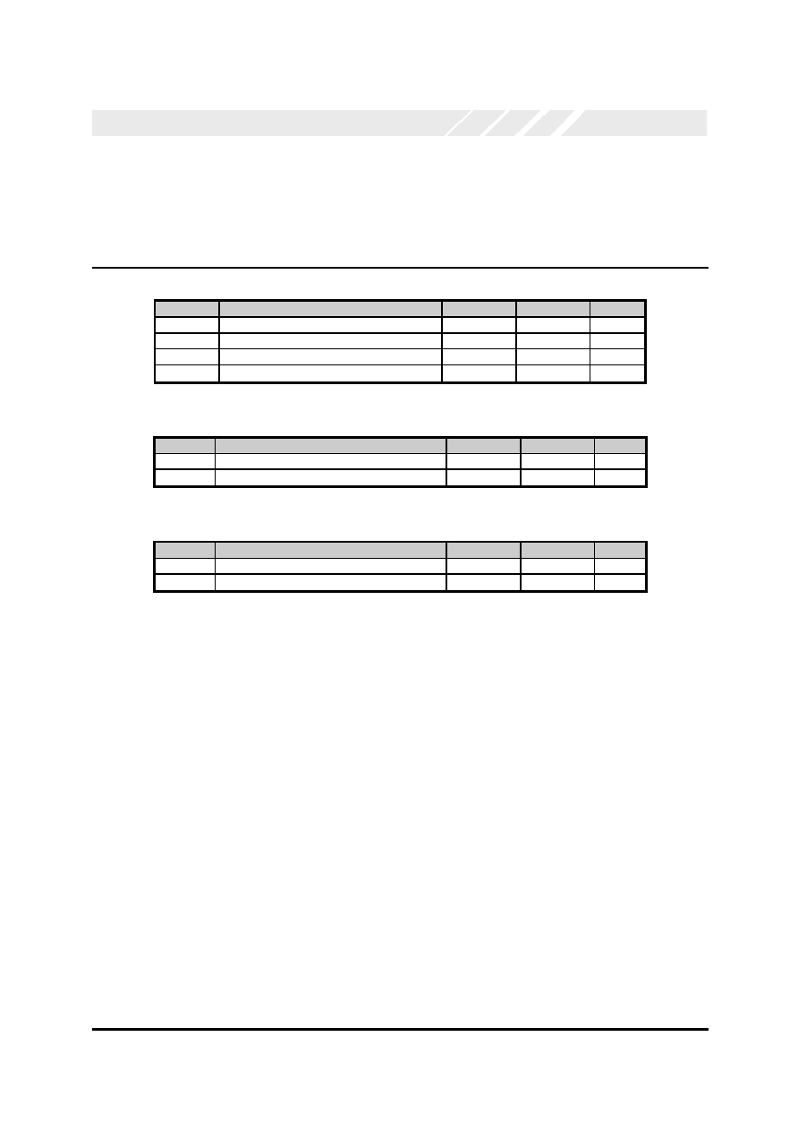
Data Sheet Revision 1.0 Page 43
OX16C954 rev B
OXFORD SEMICONDUCTOR LTD.
16 O
PERATING
C
ONDITIONS
Symbol
Parameter
Min.
Max.
Units
V
DD
DC supply voltage
-0.3
7.0
V
V
IN
DC input voltage
-0.3
V
DD
+ 0.3
V
I
IN
DC input current
+/- 10
mA
T
STG
Storage temperature
-40
125
°
C
Table 20: Absolute Maximum Ratings
Symbol
Parameter
Min
Max
Units
V
DD
DC supply voltage
4.75
5.25
V
T
O
Operating Temperature range
0
70
°
C
Table 21: Recommended 5v Operating Conditions (PLCC Package)
Symbol
Parameter
Min
Max
Units
V
DD
DC supply voltage
3.0
5.25
V
T
O
Operating Temperature range
0
70
°
C
Table 21b: Recommended Operating Conditions (TQFP Package Only)
Note: For the TQFP package, a Voltage between 3.0 to 5.25 V is possible. The I/O switching thresholds are defined for 3.0 to
3.45 V operation with VDETECT held high, and for 4.75 to 5.25V with VDETECT held low. The thresholds are not calibrated
outside these ranges, but VDETECT held high gives CMOS type I/Os that scale better with Voltage, so should be used if a
voltage between these ranges is used, but the thresholds are not guaranteed.

Data Sheet Revision 1.0 Page 44
OX16C954 rev B
OXFORD SEMICONDUCTOR LTD.
17 DC E
LECTRICAL
C
HARACTERISTICS
17.1 5V Operation
Symbol
Parameter
Condition
Min.
Max.
Units
V
DD
Supply voltage
Commercial
4.75
5.25
V
V
IH
Input high voltage
TTL Interface
Note1
TTL Schmitt trigger
2.0
2.4
V
V
IL
Input low voltage
TTL Interface
Note 1
TTL Schmitt trigger
0.8
0.6
V
C
IL
Capacitance of input buffers
5.0
pF
C
OL
Capacitance of output buffers
10.0
pF
I
IH
Input high leakage current
V
in
= V
DD
-10
10
µ
A
I
IL
Input low leakage current
V
in
= V
SS
-10
10
µ
A
V
OH
Output high voltage
I
OH
= 1
µ
A
V
DD
0.05
V
V
OH
Output high voltage
I
OH
= 4 mA
Note2
2.4
V
V
OL
Output low voltage
I
OL
= 1
µ
A
0.05
V
V
OL
Output low voltage
I
OL
= 4 mA
Note2
0.4
V
I
OZ
3-state output leakage current
-10
10
µ
A
I
ST
Static current
V
in
= V
DD
or V
SS
90
150
µ
A
Operating supply current in
normal mode
f
CK
= 1.8432 MHz
f
CK
= 7.372 MHz
f
CK
= 50.00 MHz
3
10
58
5
15
67
mA
I
CC
Operating supply current in sleep
mode
f
CK
= 1.8432 MHz
f
CK
= 7.372 MHz
f
CK
= 50.00 MHz
1.3
3.6
17.6
mA
Table 22: DC Electrical Characteristics (5v)
Note 1: All input buffers are Schmitt, with the exception of FIFOSEL, CLKSEL, INTSEL, VDETECT, I/M#.
Note 2: IOH and IOL are 12 mA for DB[7:0] and 4 mA for all other outputs.

Data Sheet Revision 1.0 Page 45
OX16C954 rev B
OXFORD SEMICONDUCTOR LTD.
17.2 3.3V Operation
These figures assume the TQFP package with VDETECT tied high for 3.3V operation
Symbol
Parameter
Condition
Min.
Max.
Units
V
DD
Supply voltage
Commercial
3.00
3.45
V
V
IH
Input high voltage
TTL Interface
Note1
TTL Schmitt trigger
0.7 V
DD
1.6
V
V
IL
Input low voltage
TTL Interface
Note 1
TTL Schmitt trigger
0.2 V
DD
1.2
V
C
IL
Capacitance of input buffers
5.0
pF
C
OL
Capacitance of output buffers
10.0
pF
I
IH
Input high leakage current
V
in
= V
DD
-10
10
µ
A
I
IL
Input low leakage current
V
in
= V
SS
-10
10
µ
A
V
OH
Output high voltage
I
OH
= 1
µ
A
V
DD
0.05
V
V
OH
Output high voltage
I
OH
= 4 mA
Note2
2.4
V
V
OL
Output low voltage
I
OL
= 1
µ
A
0.05
V
V
OL
Output low voltage
I
OL
= 4 mA
Note2
0.4
V
I
OZ
3-state output leakage current
-10
10
µ
A
I
ST
Static current
V
in
= V
DD
or V
SS
40
150
µ
A
Operating supply current in
normal mode
f
CK
= 1.8432 MHz
f
CK
= 7.372 MHz
f
CK
= 50.00 MHz
1.1
2.4
12.9
3.1
5.2
31.0
mA
I
CC
Operating supply current in sleep
mode
f
CK
= 1.8432 MHz
f
CK
= 7.372 MHz
f
CK
= 50.00 MHz
1.1
1.8
10.9
mA
Table 23: DC Electrical Characteristics (3v)
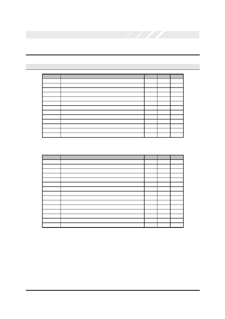
Data Sheet Revision 1.0 Page 46
OX16C954 rev B
OXFORD SEMICONDUCTOR LTD.
18 AC E
LECTRICAL
C
HARACTERISTICS
18.1 5V Operation
Symbol Parameter
Min
Max
Units
t
sa
Address set-up time to IOR# or IOW# falling
0
ns
t
ha
Address hold time after IOR# or IOW# rising
0
ns
t
sc
Chip-select set-up time to IOR# or IOW# falling
0
ns
t
hc
Chip-select hold time after IOR# or IOW# rising
0
ns
t
r1
Pulse duration of IOR#
29
ns
t
r2
Delay time between IOR# rising and IOR# or IOW# falling
43
t
acc
Data valid after IOR# falling (access time)
23
ns
t
hd
Data valid (hold) after IOR# rising
0
t
fd
Data bus floating after IOR# rising
10
ns
t
w1
Pulse duration of IOW#
29
ns
t
w2
Delay time between IOW# rising and IOR# or IOW# falling
43
ns
t
sd
Data set-up time to IOW# rising
0
ns
t
hd
Data hold time after IOW# rising
4
ns
Table 24: Data bus timing for Intel mode
Symbol Parameter
Min
Max
Units
t
sa
Address set-up time to DS# falling
5
ns
t
ha
Address hold time after DS# rising
0
ns
t
srwr
R/W# set-up time to DS# falling (read cycle)
5
ns
t
hrwr
R/W# hold time after DS# rising (read cycle)
0
ns
t
dr1
Pulse duration of DS# (read cycle)
29
ns
t
dr2
Delay to start of next read/write cycle (read cycle)
43
ns
t
acc
Read data valid after DS# falling (access time)
23
ns
t
dhr
Read data hold data after DS# rising
0
ns
t
fd
Data bus float after DS# rising
10
ns
t
srww
R/W# set-up time to DS# falling (write cycle)
5
ns
t
hrww
R/W# hold time after DS# rising (write cycle)
0
ns
t
dw1
Pulse duration of DS# (write cycle)
29
ns
t
dw2
Delay to start of next read/write cycle (write cycle)
43
ns
t
sd
Write data set-up time to DS# rising
0
ns
t
hdw
Write data valid after DS# rising
4
ns
Table 25: Data bus timing for Motorola mode:
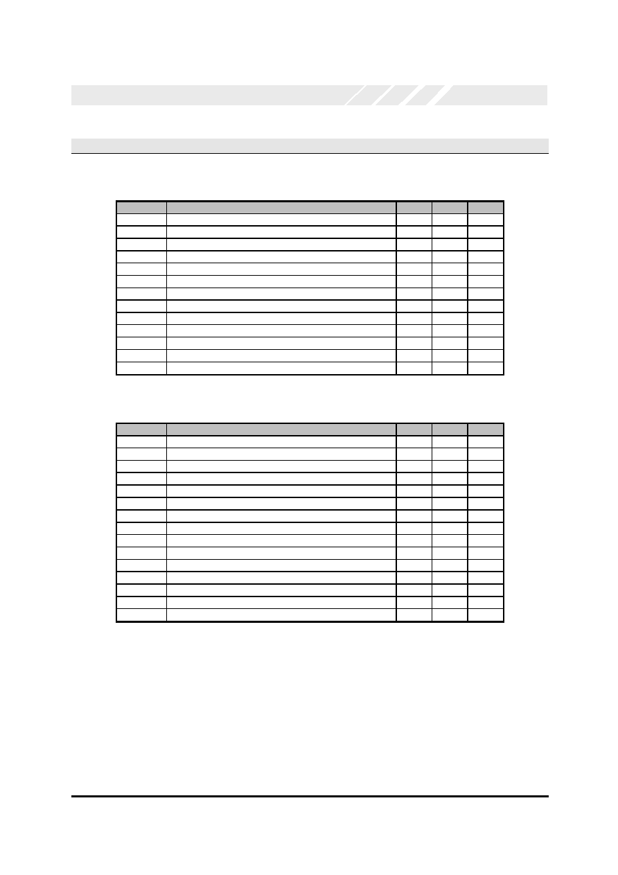
Data Sheet Revision 1.0 Page 47
OX16C954 rev B
OXFORD SEMICONDUCTOR LTD.
18.2 3.3V Operation
N.B. Maximum frequency of operation is downgraded under 3V operation to 50 MHz
Symbol Parameter
Min
Max
Units
t
sa
Address set-up time to IOR# or IOW# falling
0
ns
t
ha
Address hold time after IOR# or IOW# rising
0
ns
t
sc
Chip-select set-up time to IOR# or IOW# falling
0
ns
t
hc
Chip-select hold time after IOR# or IOW# rising
0
ns
t
r1
Pulse duration of IOR#
41
ns
t
r2
Delay time between IOR# rising and IOR# or IOW# falling
51
t
acc
Data valid after IOR# falling (access time)
32
ns
t
hd
Data valid (hold) after IOR# rising
0
t
fd
Data bus floating after IOR# rising
14
ns
t
w1
Pulse duration of IOW#
41
ns
t
w2
Delay time between IOW# rising and IOR# or IOW# falling
51
ns
t
sd
Data set-up time to IOW# rising
0
ns
t
hd
Data hold time after IOW# rising
4
ns
Table 26: Data bus timing for Intel mode
Symbol Parameter
Min
Max
Units
t
sa
Address set-up time to DS# falling
5
Ns
t
ha
Address hold time after DS# rising
0
Ns
t
srwr
R/W# set-up time to DS# falling (read cycle)
5
Ns
t
hrwr
R/W# hold time after DS# rising (read cycle)
0
Ns
t
dr1
Pulse duration of DS# (read cycle)
41
ns
t
dr2
Delay to start of next read/write cycle (read cycle)
51
ns
t
acc
Read data valid after DS# falling (access time)
32
ns
t
dhr
Read data hold data after DS# rising
0
ns
t
fd
Data bus float after DS# rising
14
ns
t
srww
R/W# set-up time to DS# falling (write cycle)
5
ns
t
hrww
R/W# hold time after DS# rising (write cycle)
0
ns
t
dw1
Pulse duration of DS# (write cycle)
41
ns
t
dw2
Delay to start of next read/write cycle (write cycle)
51
ns
t
sd
Write data set-up time to DS# rising
0
ns
t
hdw
Write data valid after DS# rising
4
ns
Table 27: Data bus timing for Motorola mode:
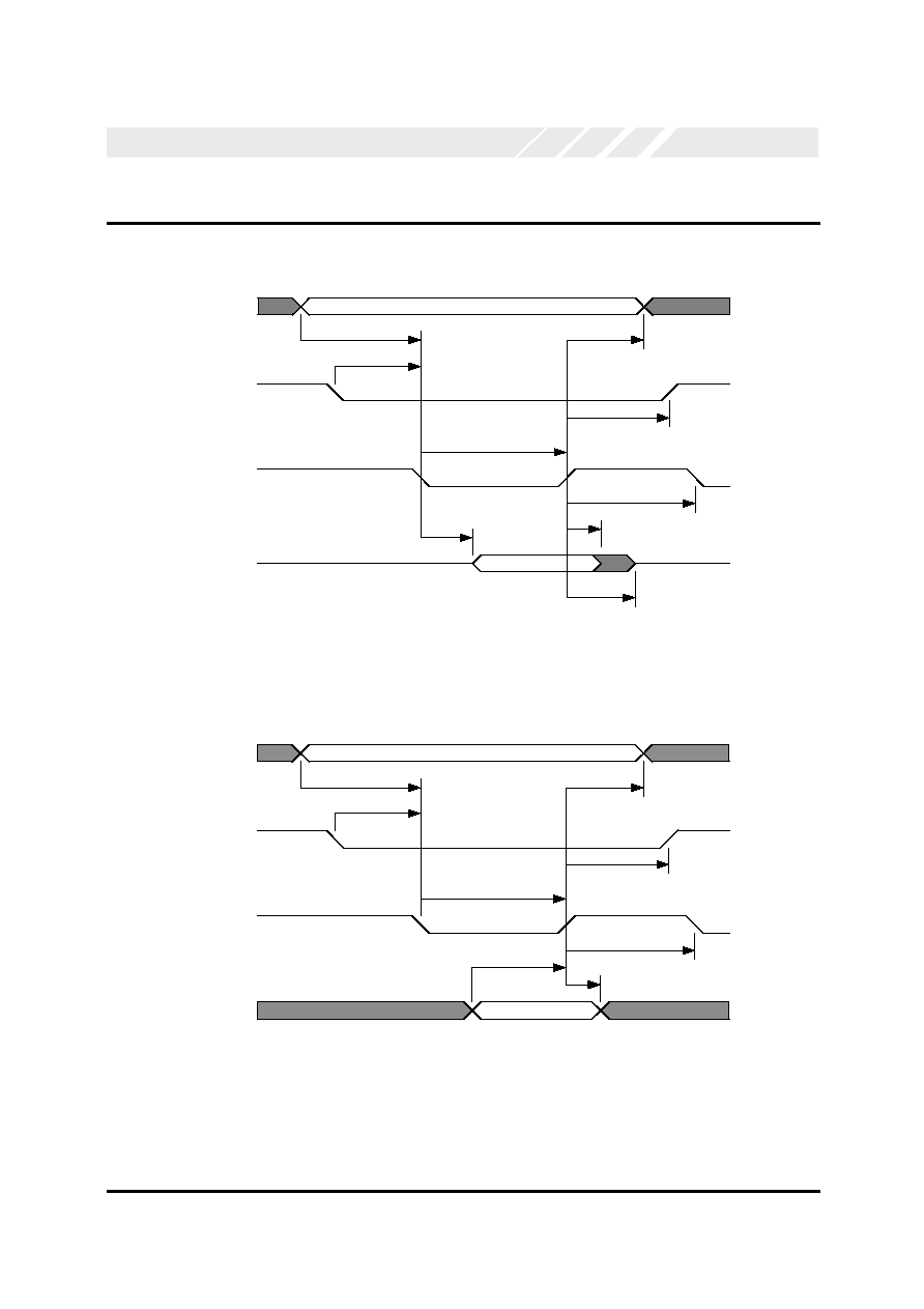
Data Sheet Revision 1.0 Page 48
OX16C954 rev B
OXFORD SEMICONDUCTOR LTD.
19 T
IMING
W
AVEFORMS
t
sc
t
sa
t
r1
t
ha
t
hc
t
acc
t
r2
t
fd
A[2:0]
CS0#, CS1#
CS2#, CS3#
IOR#
DB [7:0]
Data Valid
Address Valid
t
hd
Figure 4: Intel Mode Read Cycle Timing
t
sc
t
sa
t
w1
t
ha
t
hc
t
sd
t
w2
t
hd
A[2:0]
CS0#, CS1#
CS2#, CS3#
IOW#
DB[7:0]
Data Valid
Address Valid
Figure 5: Intel Mode Write Cycle Timing
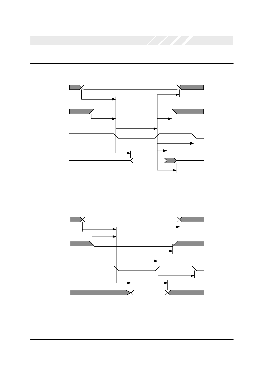
Data Sheet Revision 1.0 Page 49
OX16C954 rev B
OXFORD SEMICONDUCTOR LTD.
T
IMING
W
AVEFORMS
t
sa
t
srwr
t
dr1
t
ha
t
hrwr
t
acc
t
dr2
t
fd
A[2:0]
R/W#
DS#
DB[7:0]
Data Valid
Address Valid
t
hdr
Figure 6: Motorola Mode Read Cycle Timing
A[2:0]
R/W#
DS#
DB[7:0]
t
sa
t
srww
t
dw1
t
ha
t
hrw
w
t
sd
t
dw2
Data Valid
Address Valid
t
hd
w
Figure 7: Motorola Mode Write Cycle Timing
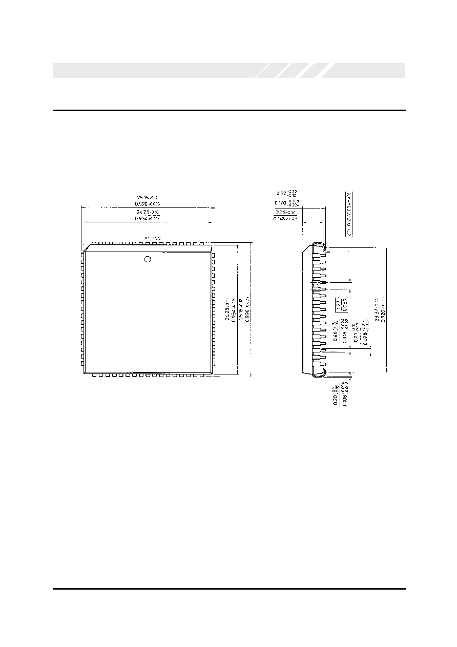
Data Sheet Revision 1.0 Page 50
OX16C954 rev B
OXFORD SEMICONDUCTOR LTD.
20 P
ACKAGE
I
NFORMATION
Figure 8: 68 Pin Plastic Leaded Chip Carrier
OX16C954-PCC60-B
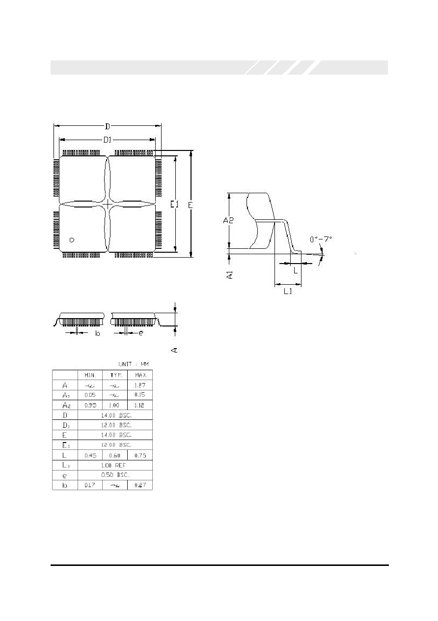
Data Sheet Revision 1.0 Page 51
OX16C954 rev B
OXFORD SEMICONDUCTOR LTD.
Figure 9: 68 Pin Plastic Leaded Chip Carrier

Data Sheet Revision 1.0 Page 52
OX16C954 rev B
OXFORD SEMICONDUCTOR LTD.
21 O
RDERING
I
NFORMATION
OX16C954-PCC60-B
Revision
Operating Conditions -Commercial
Package Type - 68
P
L
C
C
OX16C954-TQC60-B
Revision
Operating Conditions -Commercial
Package Type 80TQFP

Data Sheet Revision 1.0 Page 53
OX16C954 rev B
OXFORD SEMICONDUCTOR LTD.
N
OTES
This page has intentionally been left blank.

©Copyright Oxford Semiconductor Ltd 2001
Oxford Semiconductor Ltd believes the information contained in this document to be accurate and reliable. However, it is subject
to change without notice. No responsibility is assumed by Oxford Semiconductor for its use, nor for infringement of patents or
other rights of third parties. No part of this publication may be reproduced, or transmitted in any form or by any means without the
prior consent of Oxford Semiconductor Ltd. Oxford Semiconductor's terms and conditions of sale apply at all times.
C
ONTACT
D
ETAILS
Oxford Semiconductor Ltd.
25 Milton Park
Abingdon
Oxfordshire
OX14 4SH
United Kingdom
Telephone:
+44 (0)1235 824900
Fax:
+44 (0)1235 821141
Sales e-mail:
sales@oxsemi.com
Web site:
http://www.oxsemi.com