OZ962
03/01/00
OZ962-SF-2.7
Page 1
©
Copyright 1999 by O
2
Micro
All Rights Reserved
U.S. Patent #5,619,402
High-Efficiency Inverter Controller
FEATURES
∑
Single-stage power conversion, input voltage
range of 5V to 18V
∑
Reduces the number of components and board
size by 30% compared with conventional design
∑
Supports both floating and grounded secondary
designs
∑
90% efficiency vs. typical 75% efficiency of
conventional designs
∑
Internal open-lamp and short-circuit protections
∑
Wide dimming range
∑
Supports synchronization among multiple
inverter modules
∑
Reliable 2-winding transformer design,
eliminates arcing problems
∑
Constant frequency, symmetrical, sinusoidal
drive
ORDERING INFORMATION
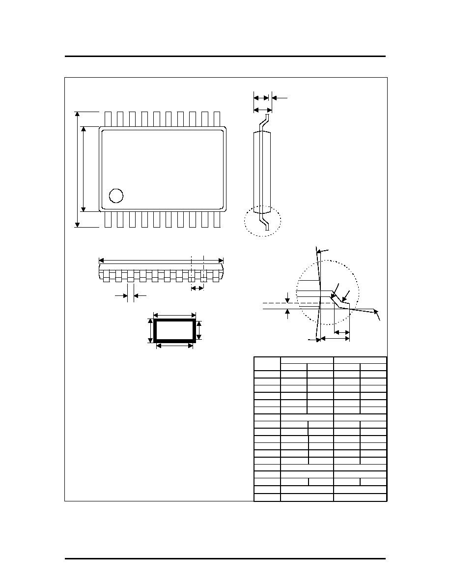
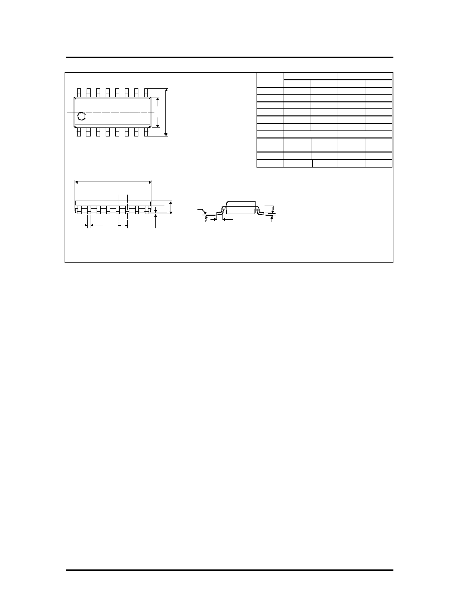
OZ962R - 16 lead TSSOP
OZ962G - 16-pin plastic SOP
GENERAL DESCRIPTION
The OZ962 is a unique high-efficiency, CCFL
backlight controller. It generates symmetrical,
near sinusoidal output voltage and current
waveforms for driving a CCFL backlight. The
OZ962 operates in a single, constant frequency,
pulse-width-modulation (PWM) mode. Typical
operating frequency ranges between 30 KHz to
100 KHz, depending on the CCFL and the
transformer's characteristics.
Operating in a PWM push-pull manner, the
transformer in the OZ962 backlight inverter
requires only one primary winding and one
secondary winding, with the secondary winding
requiring no fold-back treatment.
The OZ962 is available in both 16-pin SOIC and
TSSOP packages. It is specified over the
commercial temperature range: 0 oC to +70 oC.
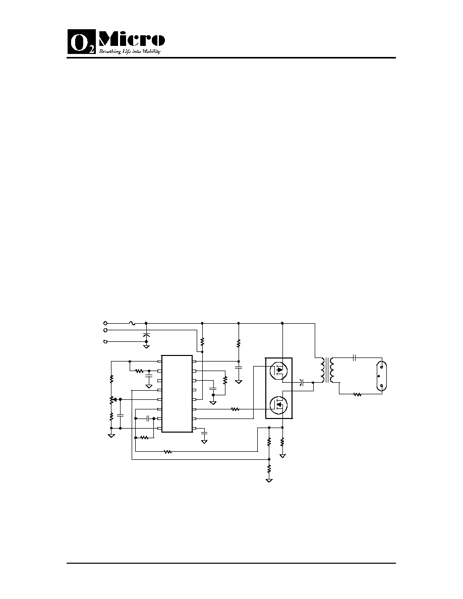
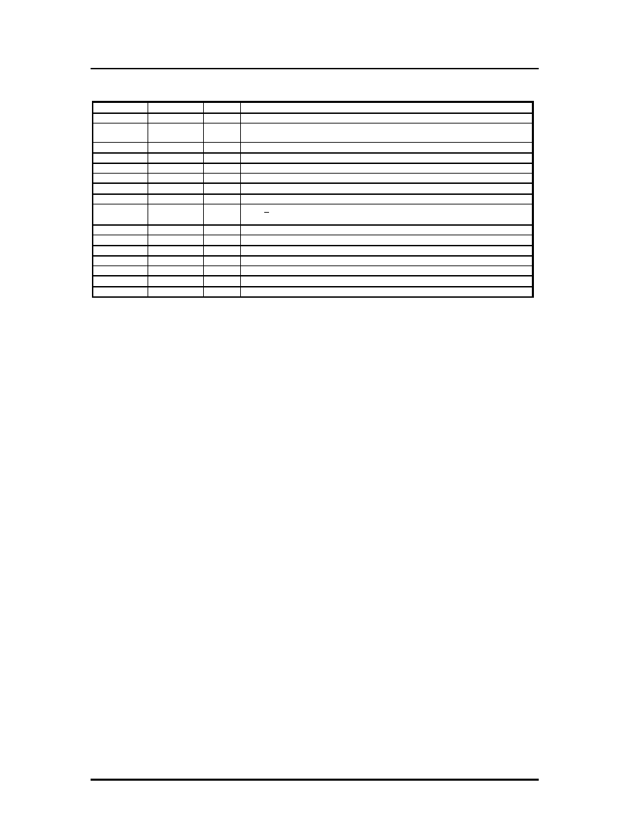
TYPICAL APPLICATION CIRCUIT
Figure 1. Typical Floating Secondary Application
Circuit
C1
22u
25V
-
+
F1
1A Fast Fuse
VDD (+12V)
ENA
GND
CN1
C3
330p
R1
220K
R2
10K
R3
5.1K
C2
0.1u
R6
30
R8
0.5
R13
100
R12
750
1.0K
R4
15K
R7
100K
C8
C5
C6 2.2u
C7
C4
0.1u
220p
0.22u
68p
3KV
50V
+
-
*
*
2200T
33T
3.5W
SI4559EY
4
1
7,8
5,6
3
U2
R5
10K
R14
OZ962G
REF
OVP
NC
SCP
ADJ
FB
CMP
GND
VDD
RT
CT
CLK
ENA
NDR
PDR
SST
1
2
3
4
5
6
7
8
9
16
15
14
13
12
11
10
U1
2
Q2
Q1
R9
200K
R10
100
C9
.01u
R11
1M
OZ962
OZ962-SF-2.7
Page 2
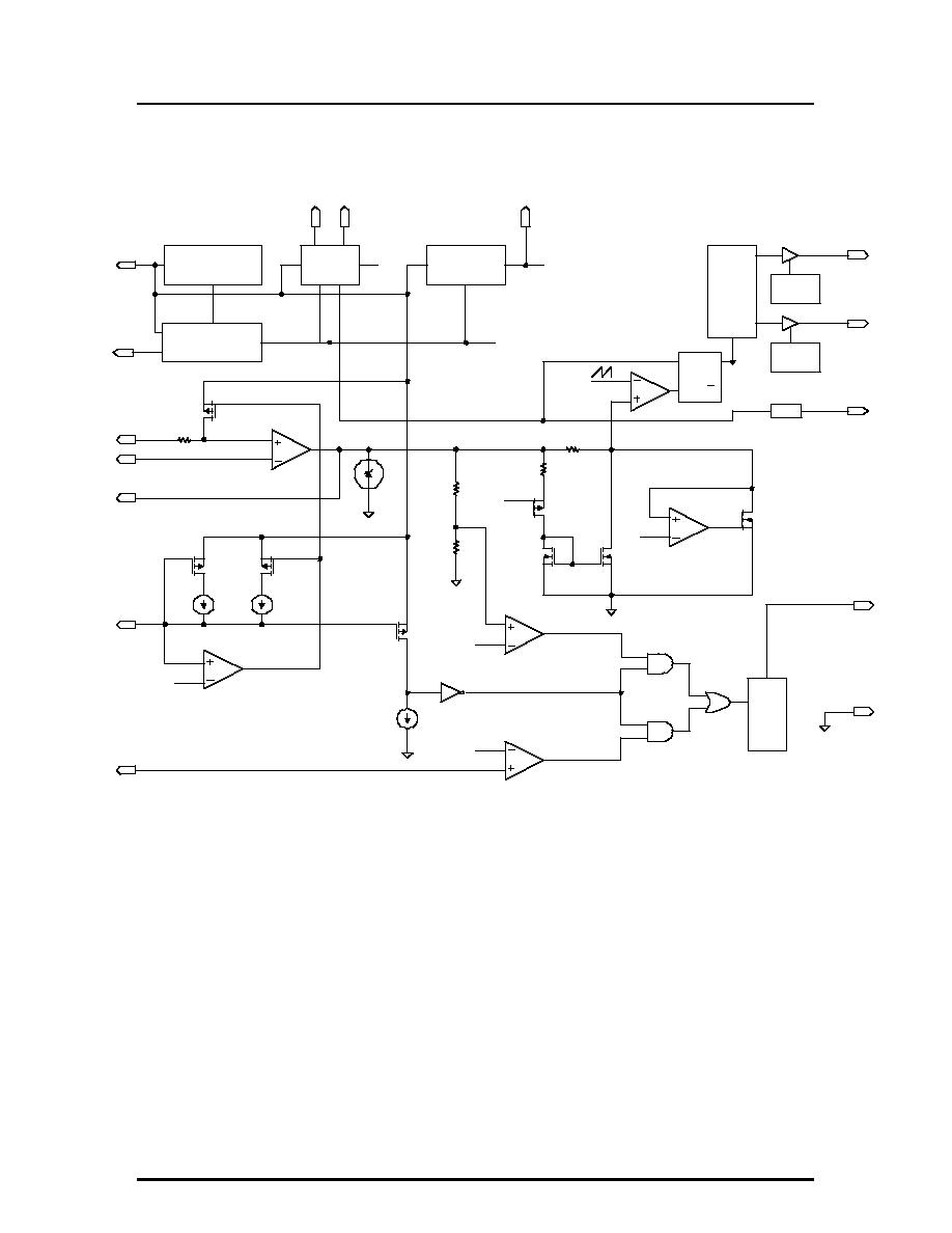
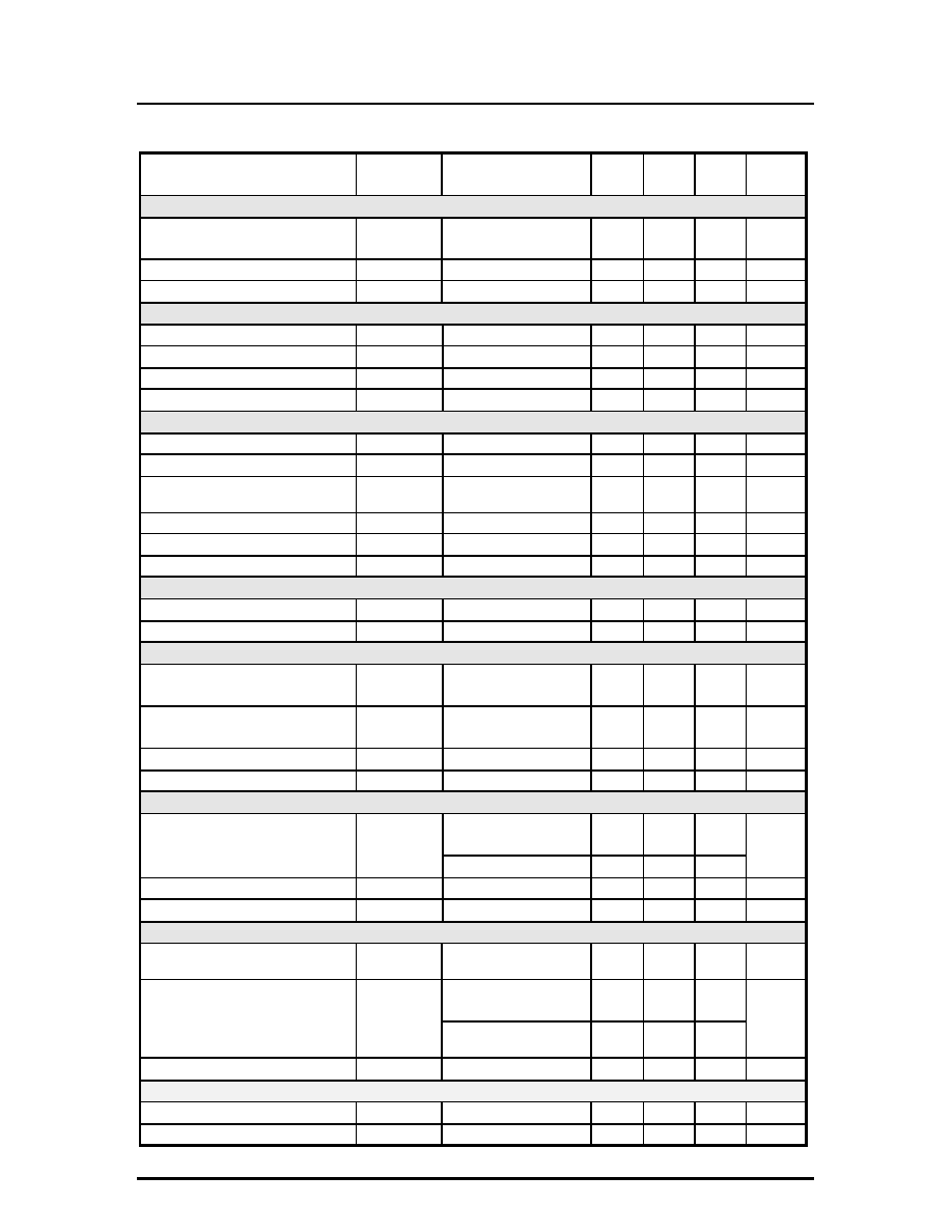
FUNCTIONAL BLOCK DIAGRAM
Note:
OVP ≠ Over Voltage Protection
SCP ≠ Short-Circuit Protection
UVL ≠ Under Voltage Lockout
Figure 2. Functional Block Diagram
Under Voltage
Lockout
Band Gap
Reference
REF(1)
VDD(16)
OSC
Ct(14) Rt(15)
RAMP
OVP Voltage
Generator
OVP(2)
OVP=Vref-(Vdd - 1)(12.5/150)
D=1.1(OVP)/2.5 - 0.2
OVP
Vref (2.5V)
ADJ(5)
FB(6)
40k
SST(9)
2.0v
3V
CMP(7)
SCP(4)
Vdd
ADJ
9k
1k
OVP
SCP & OVP inhibited during
start-up
ENA(12)
30k
60k
Ve=Vcmp-2*(Vcmp-SST-Vgs)
Ve
Dmax
Clamp
Break
Before
Make
1/2F
CLK(13)
NDR(11)
PDR(10)
SST
SST
2
µ
A
10
µ
A
3
µ
A
GND(8)
Vcmp
Error
Amp.
OVP
N-Clamp
OSC
P-Clamp
OVP
SCP
UVL
shut
down
latch
RAMP
S
Q
R
Q
OZ962
OZ962-SF-2.7
Page 3
PIN DESCRIPTION
Names
Pin No.
I/O
Description
REF
1
O
Reference voltage output. Nominal voltage is 2.5 V.
OVP
2
I
Over-voltage protection setting. Refer to formula for OVP in block diagram
on page 2 of this document.
NC
3
-
No connection.
SCP
4
I
Short-circuit protection input.
ADJ
5
I
Reference voltage input for dimming control.
FB
6
I
Current sense feedback.
CMP
7
O
Compensation for the current sense feedback.
GND
8
GND
Ground.
SST
9
I
Tsst ~ 0.2 Csst (Vdd - 5), where Csst is the soft start capacitor value in
µ
F
and Tsst value is in
µ
s.
PDR
10
O
Gate drive output for the P-MOSFET.
NDR
11
O
Gate drive output for the N-MOSFET.
ENA
12
I
Enable input, active high (Vth is about 1.7 V).
CLK
13
O
Open-drain clock output.
CT
14
I/O
Timing capacitor. CT and RT set the clock frequency.
RT
15
I/O
Timing resistor.
VDD
16
PWR
Supply voltage input.
ABSOLUTE MAXIMUM RATINGS
VDD
18 V
GND
+/- 0.3 V
Logic inputs
-0.3 V to VDD+0.3 V
Power dissipation
800 mW at 25
o
C
Operating temp.
0
o
C to 70
o
C
Operating junction temp.
150
o
C
Storage temp.
-55 to 150
o
C
RECOMMENDED OPERATING RANGE
VDD
5V to 18V
Fosc
30 KHz to 100 KHz
Rosc
50 k to 150 k
OZ962
OZ962-SF-2.7
Page 4
FUNCTIONAL SPECIFICATIONS
Parameter
Symbol
Test Conditions
Limits
Unit
5 V < VDD < 15 V
Min
Typ
Max
Reference Voltage
Nominal voltage
Vref
I
load
= 0.25 mA,
VDD = 5 V
2.37
2.50
2.63
V
Line regulation
-
8
-
mV/V
Load regulation
I
load
= 0.2 mA to 1.0 mA
-
1
-
mV/mA
Oscillator
Initial accuracy
fosc
Ct = 220 pF, Rt = 120 k
48
53
58
KHz
Ramp peak
2.45
2.55
2.65
V
Ramp valley
0.40
0.45
0.50
V
Temp. stability
TA = 0
o
C to 70
o
C
-
-
200
ppm/
o
C
Error Amplifier
Input bias current
V
ADJ
=V
FB
=2.0 V
-
25
500
nA
Input offset voltage
V
FB
= 4.0 V
-
5
10
mV
Input voltage range
0
-
VDD-
1.5
V
Open loop voltage gain
50
60
-
dB
Unity gain bandwidth
1
1.5
-
MHz
Power supply rejection
50
60
-
dB
Under-Voltage Lockout
Positive-going threshold voltage
-
3.8
4
V
Negative-going threshold voltage
3.4
3.6
-
V
Supply
Supply current - Enable Low
Adj, CT = Open
I
OFF
VDD
= 5.0 V
-
25
120
µ
A
Supply current - Enable Low
Adj, CT = Open
I
OFF
VDD
= 15 V
-
25
120
µ
A
Supply current - Enable High
I
ON
VDD
= 5.0 V
-
0.6
1.5
mA
Supply current - Enable High
I
ON
VDD
= 15 V
-
0.6
1.5
mA
NDR output
Output high voltage
V
OH
Isink = 10 mA,
VDD < 7.8 V
VDD-
0.3
VDD-
0.5
-
V
VDD >7.8 V
7.0
8.0
9.0
V
Output low voltage
V
OL
Isource = 10 mA
-
0.3
0.8
V
Output resistance
R
OUT
VDD
= 5.0 V
-
50
80
PDR output
Output high voltage
V
OH
Isink = 10 mA
VDD-
0.6
VDD-
0.3
-
V
Output low voltage
V
OL
Isource = 10 mA,
VDD < 7.8 V
0.4
0.5
0.8
V
VDD > 7.8 V
-
VDD-
6.0
VDD-
4.0
Output resistance
R
OUT
VDD
= 5.0 V
-
50
80
Break-Before-Make
Qn off to Qp on delay
T
HL
200
240
280
ns
Qp off to Qn on delay
T
LH
220
260
300
ns