 | –≠–ª–µ–∫—Ç—Ä–æ–Ω–Ω—ã–π –∫–æ–º–ø–æ–Ω–µ–Ω—Ç: OZ990S | –°–∫–∞—á–∞—Ç—å:  PDF PDF  ZIP ZIP |

OZ990
07/13/00 OZ990-SF-1.6
Page
1
Copyright 1998 by O
2
Micro
All Rights Reserved
Intelligent Manager
Smart PMU/GPIO
FEATURES
∑
SMBus 1.0 Compliant
∑
Support Pentium class and x86-based designs
∑
PMU, GPIO, and Alternative PMU modes
∑
WAKE output and Suspend Status input operates
synchronously with PMU in notebook chipsets
∑
LOW power-saving Suspend mode
∑
Hardware Debounced Wakeup/Suspend input as
pushbutton
∑
4 Power Control programmable outputs with built-
in Power Sequencing at 10 ms to 1 second
programmable intervals
∑
Optional Wakeup-Disable inputs
∑
Optional Power-On inputs
∑
8 programmable interrupt inputs for SMIEVENT
or SMBALERT#
∑
8 Suspend/Wakeup edge-triggered
programmable inputs
∑
20 possible programmable edge-sensitive
General Purpose Inputs/Outputs
∑
8 Auto LED Flash(ALF) programmable outputs
with 10% or 50% duty cycles
∑
LOW power hardware driven speaker alarm
output
∑
Up to 6 programmable unique addresses for
device cascade
∑
8 power-on modularized hardware ID
programmable inputs
∑
32KHz operating frequency
∑
5 V tolerant inputs
∑
Supports both 3.3 V and 5 V operating
environments
∑
Software programming kit available
ORDERING INFORMATION
OZ990S - 28 SSOP
GENERAL DESCRIPTION
O
2
Micro's OZ990 Smart PMU/GPIO (Power
Management Unit/General Purpose Input Output) unit
allows the implementation of Green PC Desktop
Chipsets in notebook designs at considerably lower
cost than conventional methods while closing the
technology gap between desktop and notebook
computers by offering an extensive number of
powerful power management and general purpose I/O
features. With the OZ990 stand-alone PMU capability,
the ability to provide the One-Shot Design for
PMU/BIOS practically eliminates the need to redesign
PMUs to match the ever-changing core logic chipsets.
The OZ990 provides the perfect solution for leading
notebook vendors to stay ahead of the competition.
The OZ990 is an SMBus 1.0 compliant device with 4
Power Control and 16 Programmable General
Purpose I/Os pins flexible for a variety of functions
such as Power Control with sequencing,
programmable inputs/outputs, SMB/SMI interrupt
service, power-saving, Suspend/Wakeup,
modularized hardware ID, and Auto LED Flash (ALF)
status display. Other features include hardware-driven
speaker alarm output and Suspend/Wakeup button.
As a Pentium class and x86-based system compatible
device, the OZ990 is a highly cost-effective and
practical solution for today's notebook and palmtop
computers, pen-based data systems, personal digital
assistants, and portable data-collection terminals.

OZ990
OZ990-SF-1.6
Page
2
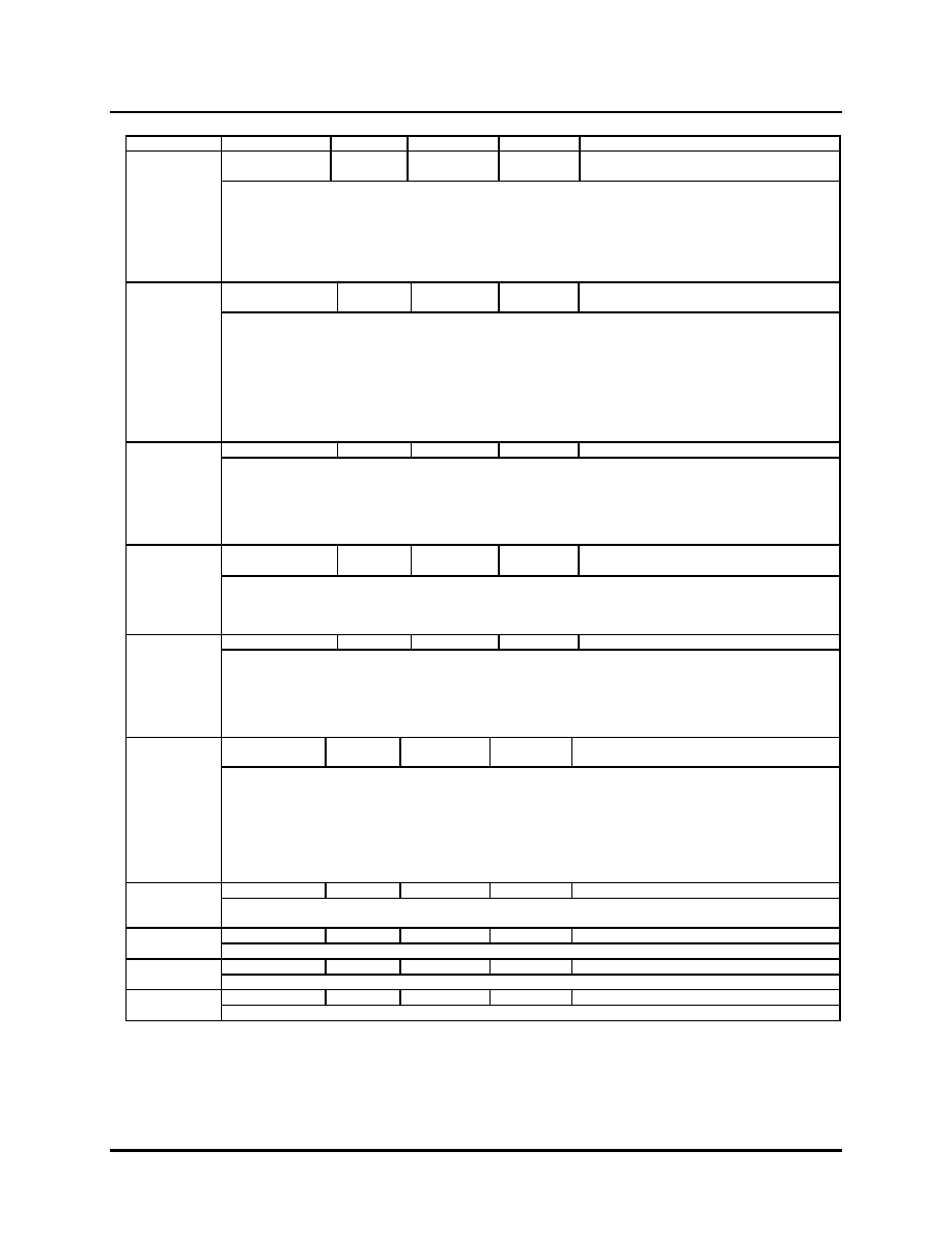
PIN ASSIGNMENT
PIN CONFIGURATION
Name Pin
No. Type Input Drive
Definition
SMBCLK
1 I
TTL -
SMBus Clock Input
SMBus Clock Input for SMBus protocol communication.
SMBDATA
2 I/O
TTL
12mA
SMBus Data Input/Output
SMBus Data Input/Output for SMBus protocol communication.
PWRGD
3 I
TTL -
Host System Power Good
This pin indicates that the host system's power, including the Core Logic chipsets, is stable. Before the host
system's power is stable, this input pin will tri-state all the output pins from OZ990 with the exception of the
Power Control pins. The state of the PWRGD pin determines whether the OZ990 is in PMU or Alternate
PMU mode when RESETN is active. When pin MODE=1 and pin PWRGD=0, the OZ990 is in PMU mode.
When pin MODE=1 and pin PWRGD=1, the OZ990 is in Alternate PMU mode.
MODE
4 I
TTL -
OZ990 Mode Input
The OZ990 has 3 modes of operation: GPIO(with 20 GPIOs available), PMU(with 16 GPIOs available), and
Alternate PMU(with 16 GPIOs available). To use the OZ990 as a PMU, tie MODE pin to VDD and set
PWRGD LOW. For Alternate PMU mode, tie MODE pin to VDD and set PWRGD HIGH. For GPIO-only
mode, tie MODE pin LOW. Refer to MODE description for more details.
PC[3:0]/
GPIO[19:16]
[8:5]
I/O
TTL
4mA
Power Control Outputs /
General Purpose I/Os
Pins PC[3:0]/GPIO[19:16] can be used as Power Control outputs for cold start, reset, Suspend, and Wakeup
or as regular GPIOs. Upon power up, if the OZ990 is in PMU mode, PC[3:0] will default to 0, with OZ990
initially in Suspend mode. By default, on a falling edge-triggered SRBTN#/GPIO[15] (with Wakeup function),
PC[3:0] will be set to 1 to power on the system. On a subsequent trigger of GPIO[15:8]'s Suspend and
Wakeup functions, the values in PC_SUSPEND[3:0] and PC_WAKE[3:0] in register 0Bh will be copied onto
the PC[3:0] output pins. Additionally, the OZ990 provides a power sequencing feature that allows up to 8
different programmable values of staggering time for the PC[3:0] outputs. PC[3:0] are also programmable
just like the GPIO[19:16] pins but with bits PCI[3:0] in register 0Bh as input data and PCO[3:0] in register
0Ch as output data values.
GPIO[0]/
SMIEVENT
9 I/O
TTL
4mA
General Purpose I/O /
SMIEVENT
Fully programmable GPIOs that can be used for a variety of dedicated or specific functions. Pin GPIO[0] has
SMIEVENT output as an alternate function. GPIO[0] defaults as outputs in PMU mode, and as input in
Alternate PMU and GPIO modes. It is also programmable to function as either GPI[0] input, GPO[0]output,
ALF[0] output, PWRON input, WAKE_DIS input, or ID[0] input(in Alternate PMU and GPIO modes). When
implementing as ID[0] input, GPIO[0]/SMIEVENT pin is internally latched from external pull-ups or pull-
downs, when RESETN is LOW. The values will be stored permanently in the ID Register and
GPIO[0]/SMIEVENT pin can then be reconfigured as an output. Refer to GPIO Config.1&2 Registers for
more details and GPIO Config. Tables for input/output selections.
1
2
3
4
5
6
7
8
9
10
11
12
13
14
28
27
26
25
24
23
22
21
20
19
18
17
16
15
SMBCLK
SMBDATA
PWRGD
MODE
PC[0] / GPIO[16]
PC[1] / GPIO[17]
PC[2] / GPIO[18]
PC[3] / GPIO[19]
GPIO[0] / SMIEVENT
GPIO[1] / WAKE
GPIO[2] / SMBALERT#
GPIO[3]
GPIO[4]
GND
VCC
32KHZ
RESETN
SRBTN # / GPIO[15]
GPIO[14]
GPIO[13]
GPIO[12]
GPIO[11]
GPIO[10]
GPIO[9]
GPIO[8]
SMBIDSEL[2] / GPO[7]
SMBIDSEL ]1] / GPO[6]
SMBIDSEL[0] / GPO [5]
OZ990
OZ990-SF-1.6
Page
3
Name Pin
No.
Type
Input
Drive
Definition
GPIO[1]/
WAKE
10 I/O
TTL
4mA
General Purpose I/O /
WAKE
Fully programmable GPIO that can be used for a variety of dedicated or specific functions. Pin GPIO[1] has
WAKE output as an alternate function. GPIO[1] pin defaults as WAKE output in PMU mode, and as input in
Alternate PMU and GPIO modes. It is also programmable to function as GPI[1] input, GPO[1]output, ALF[1]
output, PWRON input, WAKE_DIS input, or ID[1] input. When implementing as ID[1] input, GPIO[1]/WAKE
pin is internally latched from external pull-ups or pull-downs, when RESETN is LOW. The values will be
stored permanently in the ID Register and GPIO[1]/WAKE pin can then be reconfigured as an output. Refer
to GPIO Config.1&2 Registers for more details and GPIO Config. Tables for input/output selections.
GPIO[2]/
SMBALERT#
11 I/O
TTL
4mA
General Purpose I/O /
SMBALERT#
Fully programmable GPIO that can be used for a variety of dedicated or specific functions. Pin GPIO[2]
defaults as input in all modes. This pin, when programmed as an alternate function, can generate the
SMBALERT# interrupt. SMBALERT# is an interrupt service request signal to the SMBus Host which can be
generated by all devices connected to the OZ990. Pin GPIO[2]/SMBALERT# is also programmable to
function as either GPI[2] input, GPO[2] output, ALF[2] output, PWRON input, WAKE_DIS input, or ID[2] input.
When implementing as ID[2] input, GPIO[2]/SMBALERT# pin is internally latched from external pull-ups or
pull-downs, when RESETN is LOW. The latched values will be stored permanently in the ID Register and
GPIO[2] pin can then be reconfigured as an output. Refer to GPIO Config.1&2 Registers for more details and
GPIO Config. Tables for I/O selections.
GPIO[4:3]
[13:12] I/O
TTL
4mA
General Purpose I/Os
Fully programmable GPIOs that can be used for a variety of dedicated or specific functions. Pins GPIO[4:3]
default as inputs in all modes. They are programmable to function as GPI[4:3] inputs, GPO[4:3] outputs,
ALF[4:3] outputs, PWRON inputs, WAKE_DIS inputs, or ID[4:3] inputs. When implemented as ID[4:3] inputs,
GPIO[4:3] pins are internally latched from external pull-ups or pull-downs, when RESETN is LOW. The
values will be stored permanently in the ID Register. GPIO[4:3] pins can then be reconfigured as outputs.
Refer to GPIO Config.1&2 Registers for more details and GPIO Config. Tables for input/output selections.
[17:15] I/O-U
TTL 4mA
SMBus ID Selects/
General Purpose Outputs
SMBIDSEL
[2:0]/
GPO[7:5]
Fully programmable GPIO that can be used for a variety of dedicated or specific functions. Pin
SMBIDSEL[2:0]/GPO[7:5] defaults as an input in all modes. Upon power on, when RESETN is LOW, these
pins are internally latched to determine which SMBus address is used for the OZ990. It is also programmable
to function as either GPO[7:5] or ALF[7:5] outputs.
GPIO[14:8]
[24:18] I/O
TTL
4mA
General Purpose I/Os
Fully programmable GPIOs that can be used for a variety of dedicated or specific functions. Pins GPIO[14:8]
default as inputs in all modes. Pins GPIO[14:8] as inputs are programmable to generate SMI/SMB interrupts
and WAKE signal(pin GPIO[1]), to enter Suspend mode, or to resume Wakeup mode from Suspend
(with/without interrupt generation). They are also programmable to function as GPI[14:8] inputs, GPO[14:8]
outputs, PWRON inputs, or WAKE_DIS inputs. Refer to GPIO Config.1&2 Registers for more details and
GPIO Config. Tables for input/output selections.
SRBTN#/
GPIO[15]
25 I/O
TTL
4mA Suspend/Resume Button /
General Purpose I/O
Fully programmable GPIO that can be used for a variety of dedicated or specific functions. In PMU mode, this
pin defaults as SRBTN# with a debounced input with "Wakeup" function triggered on the falling edge to turn
on pins PC[3:0] (PC[3:0]=1). This pin can be tied to a pushbutton to toggle between Suspend/Wakeup
modes. In Alternate PMU and GPIO modes, pin GPIO[15] defaults as input. This pin is programmable to
generate an SMB/SMI interrupt and WAKE signal(pin GPIO[1]), to enter Suspend mode, resume Wakeup
mode from Suspend (with/without interrupt generation). This pin is also programmable to function as GPI[15]
input, GPO[15] output, PWRON input, or WAKE_DIS input. Refer to GPIO Config.1&2 Registers for more
details and GPIO Config. Tables for input/output selections.
RESETN
26 I
TTL
-
Reset
OZ990 hardware reset. RESETN(active LOW) resets all registers to their default values. This pin is
connected to the RC delay from the power supplied to OZ990.
32KHz
27 I
TTL
-
32KHz Clock Input
32KHz Clock Input.
GND
14 GND -
-
Ground
Ground.
VCC
28 PWR -
-
3.3V/5V Power Supply
3.3V or 5V Power Supply.

OZ990
OZ990-SF-1.6
Page
4
GPIO PINS ALTERNATE USAGE
Name
Default Usage
Alternate Usage
PMU Mode
Alt PMU mode
GPIO mode
MODE=1
PWRGD=0
MODE=1
PWRGD=1
MODE=0
PC[0] / GPIO[16]
PCO[0]
PCO[0]
GPI[16]
GPI[16], GPO[16]
PC[1] / GPIO[17]
PCO[1]
PCO[1]
GPI[17]
GPI[17], GPO[17]
PC[2] / GPIO[18]
PCO[2]
PCO[2]
GPI[18]
GPI[18], GPO[18]
PC[3] / GPIO[19]
PCO[3]
PCO[3]
GPI[19]
GPI[19], GPO[19]
GPIO[0]/SMIEVENT
GPO[0] (SMIEVENT)
GPI[0]
GPI[0]
GPI[0], GPO[0]
ALF[0]
ID[0]
DIS_WAKE
PWRON
GPIO[1]/WAKE
GPO[1] (WAKE)
GPI[1]
GPI[1]
GPI[1], GPO[1]
ALF[1]
ID[1]
DIS_WAKE
PWRON
GPIO[2]/SMBALERT# GPI[2]
GPI[2]
GPI[2]
SMBALERT#
GPO[2]
ALF[2]
ID[2]
DIS_WAKE
PWRON
GPIO[3] GPI[3] GPI[3]
GPI[3] GPO[3]
ALF[3]
ID[3]
DIS_WAKE
PWRON
GPIO[4] GPI[4] GPI[4]
GPI[4] GPO[4]
ALF[4]
ID[4]
DIS_WAKE
PWRON
SMBIDSEL[0]/GPO[5] GPI[5]
GPI[5]
GPI[5]
GPO[5]
ALF[5]
SMBIDSEL[1]/GPO[6] GPI[6]
GPI[6]
GPI[6]
GPO[6]
ALF[6]
SMBIDSEL[2]/GPO[7] GPI[7]
GPI[7]
GPI[7]
GPO[7]
ALF[7]
GPIO[8] GPI[8] GPI[8]
GPI[8] GPO[8]
DIS_WAKE
PWRON
GPIO[9] GPI[9] GPI[9]
GPI[9] GPO[9]
DIS_WAKE
PWRON
GPIO[10] GPI[10] GPI[10]
GPI[10] GPO[10]
DIS_WAKE
PWRON
GPIO[11] GPI[11] GPI[11]
GPI[11] GPO[11]
DIS_WAKE
PWRON
GPIO[12] GPI[12] GPI[12]
GPI[12] GPO[12]
DIS_WAKE
PWRON
GPIO[13] GPI[13] GPI[13]
GPI[13] GPO[13]
DIS_WAKE
PWRON
GPIO[14] GPI[14] GPI[14]
GPI[14] GPO[14]
DIS_WAKE
PWRON
SRBTN#/GPIO[15] GPI[15]
(has
`Wake-
up' function)
GPI[15] GPI[15]
GPO[15]
DIS_WAKE
PWRON
Note: GPI[15:8] are SMI/SMB interruptible.
OZ990
OZ990-SF-1.6
Page
5
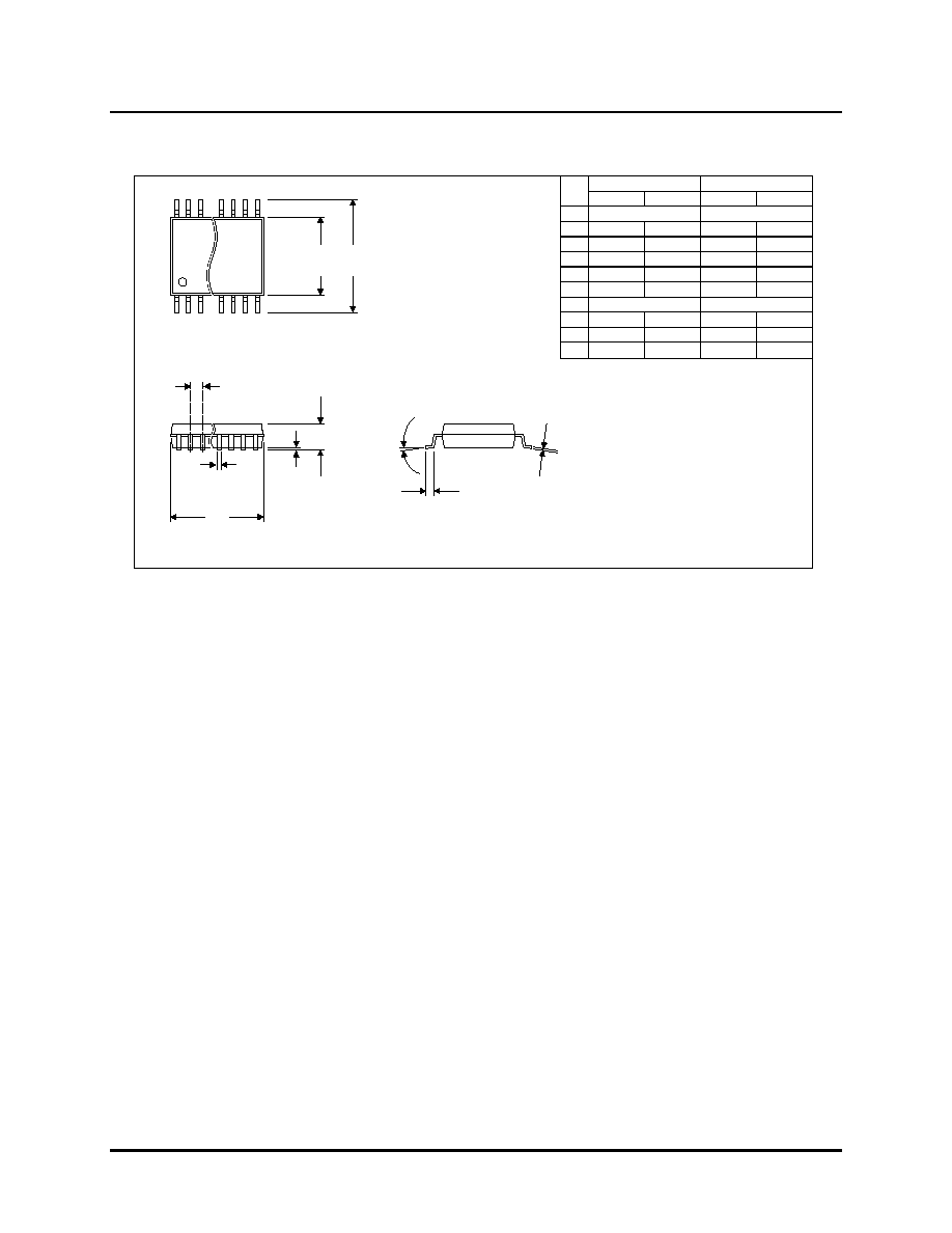
OZ990 PACKAGE INFORMATION
D
L
C
A
A1
D
B
e
E
H
SSOP
PACKAGE
(209 mil)
INCHES MILLIMETERS
DIM
MIN MAX MIN MAX
A 0.084
2.13
A1 0.002 0.010 0.05
0.25
B 0.009 0.015 0.22 0.38
C 0.004 0.008 0.09 0.20
D 0.390 0.413 9.90 10.50
E 0.197 0.220 5.00 5.60
e 0.0256
0.65
H 0.291 0.323 7.40 8.20
L 0.025 0.041 0.63 1.03
0
∞
8
∞
0
∞
8
∞