 | ÐлекÑÑоннÑй компоненÑ: OZ998S | СкаÑаÑÑ:  PDF PDF  ZIP ZIP |
Äîêóìåíòàöèÿ è îïèñàíèÿ www.docs.chipfind.ru

OZ998
07/13/00 OZ998-SF-2.2
Page
1
©Copyright 2000 by O
2
Micro
All Rights Reserved
Intelligent Manager
Smart Multi-DIMM Selector
FEATURES
·
SMBus, version 1.0, compliant
·
Intel PAS Protected Storage support
·
Support Pentium and x86-based designs
·
Support SMBus Q-Buffering via PWRGD
·
Support SMBus selector for dual/triple DIMMs
·
32KHZ input clock or Crystal input
·
Support 2 different power planes
·
10 bytes scratch pad registers
·
20 possible edge-sensitive programmable GPIOs
per device
·
8 possible Open Drain, Open Collector outputs
·
Programmable addresses for cascaded OZ998s
·
Supports 3.3V or 5V operation
·
Supports 5V tolerant LVTTL inputs (OZ998B)
·
LOW power hardware-driven speaker alarm
outputs
·
SMBALERT# and SMI event outputs
·
8 programmable interrupt inputs for SMI event or
SMBALERT#
·
8 Auto LED Flash (ALF) programmable outputs
with 10% or 50% duty cycles
ORDERING INFORMATION
OZ998S - 28 pin SSOP
GENERAL DESCRIPTION
O
2
Micro's OZ998 Multi-DIMM Selector supports the
switching between a primary SMBus and 3 other
secondary SMBus. This function is particularly useful
for DIMM devices and the support of Intel's PAS
(Preboot Authentication Service).
In addition, the OZ998 can be configured to support
two different power planes with different sets of
General Purpose Input/Output (GPIO) signals, which
supplements and enhances the power management
capability of the chipsets, commonly found in an ACPI
(Advanced Configuration of Power Interface)
subsystem.
Up to 20 possible GPIOs are available per device,
and among those, GPIO[15:8] are programmable to
be either positive or negative-edged triggers to
generate an SMIEVENT/SMBALERT# to the system.
GPIO[7:0] are programmable to be either a regular
TTL level output, open drain or open collector output.
To support over 20 GPIOs through cascading multiple
OZ998 devices, configure each individual OZ998
device ID. Up to 8 Auto LED Flash (ALF) are available
to drive an LED or speaker at a programmable
frequency.
The OZ998 is packaged in a low profile, small 28 pin
SSOP.
OZ998
OZ998-SF-2.2
Page
2
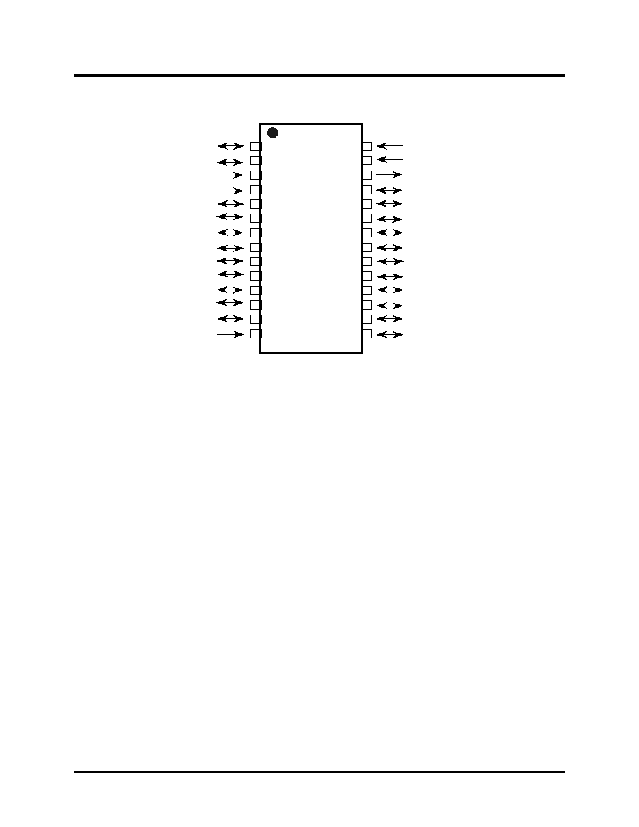
PIN DIAGRAM
OZ998
P_SMBCLK
P_SMBDATA
PWRGD
RESET#
GPIO[16]/S_SMBCLK1
GPIO[17]/S_SMBDATA1
GPIO[18]/S_SMBCLK2
GPIO[19]/S_SMBDATA2
GPIO[0]/SMIEVENT/ID[0]
GPIO[1]/ID[1]
GPIO[2]/SMBALERT#/ID[2]
GPIO[3]/ID[3]
GPIO[4]/ID[4]
GND
VCC
XIN/32KHZ
XOUT
GPIO[15]/S_SMBCLK3
GPIO[14]/S_SMBDATA3
GPIO[13]/SMB_SEL[1]
GPIO[12]/SMB_SEL[0]
GPIO[11]
GPIO[10]
GPIO[9]
GPIO[8]
GPIO[7]/ID[7]
GPIO[6]/ID[6]
GPIO[5]/ID[5]
1
2
3
4
5
6
7
8
9
10
11
12
13
14
28
27
26
25
24
23
22
21
20
19
18
17
16
15
OZ998
OZ998-SF-2.2
Page
3
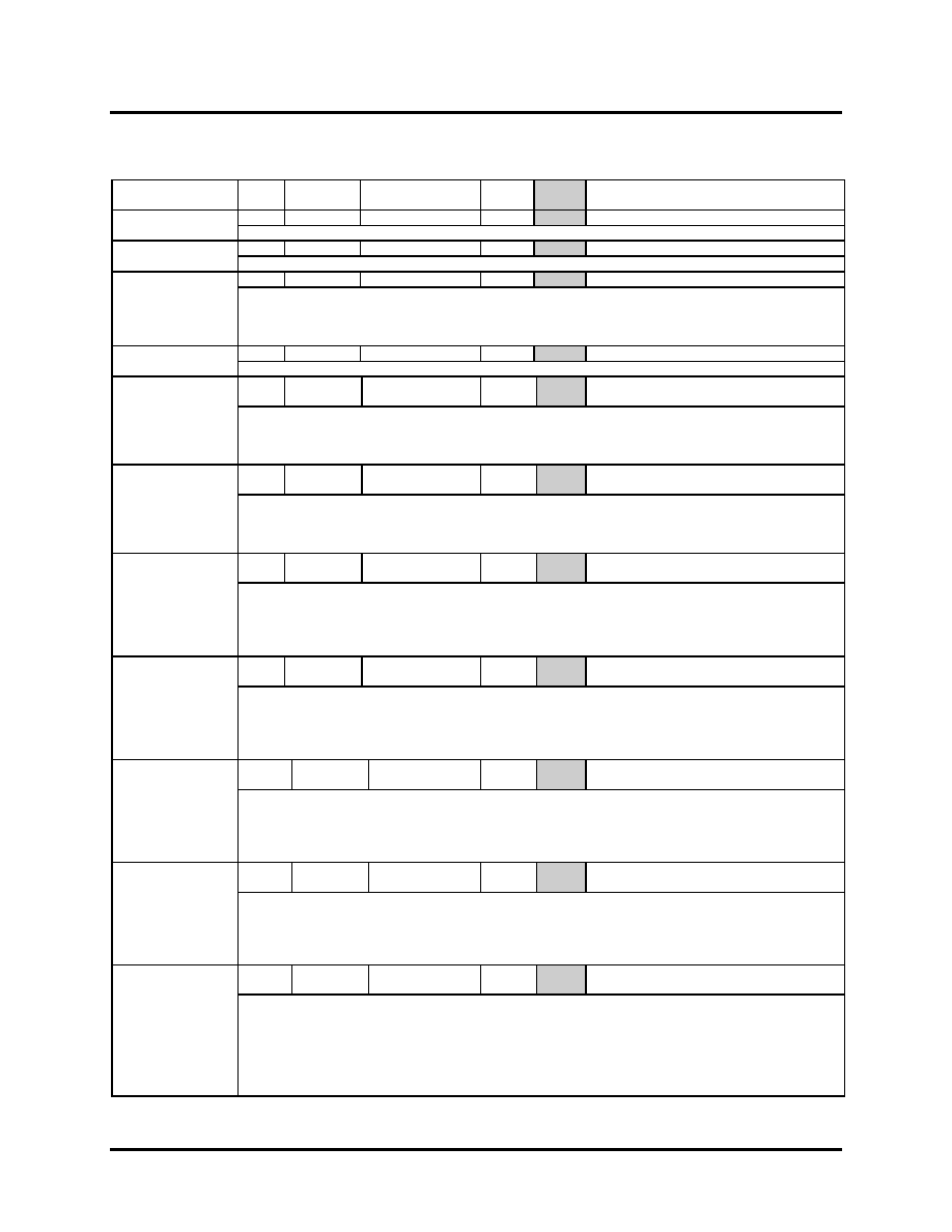
PIN DESCRIPTION
Name Pin
No.
Type Input
Drive
Definition
P_SMBCLK
1 I 3.3V/5V
Ext-PU
-
Primary SMBus Clock Input
Primary SMBus Clock Input for SMBus protocol communication.
P_SMBDATA
2 I/O 3.3V/5V
Ext-PU
12mA
Primary SMBus Data I/O
Primary SMBus Data Input/Output for SMBus protocol communication.
PWRGD
3 I
TTL
-
Host System Power Good
This pin indicates that the host system's power, including the Core Logic chipsets, is stable. Before the
host system's power is stable, this input pin will tri-state the output pins, GPO[19:8], from OZ998 while
GPO[7:0] will maintain its original value. Upon PWRGD going Low, the Secondary SMBus will be
disconnected from the Primary SMBus.
RESET#
4 I
TTL
-
Reset
This active low pin will reset the OZ998.
GPIO[16]/
S_SMBCLK1
5
I/O
TTL
4mA
General Purpose I/O/
Secondary SMBus-1 Clock I/O
Fully programmable GPIO that can be used for a variety of dedicated or specific functions. Pin GPIO[16] is
defaulted as an input. It is programmable to function as GPI[16] input, GPO[16] output or secondary
SMBus-1 Clock Input/Output. Refer to GPIO[19:16] Config.1&2 Registers for more details and GPIO
Config. Tables (section 8) for input/output selections.
GPIO[17]/
S_SMBDATA1
6
I/O
TTL
4mA
General Purpose I/O/
Secondary SMBus-1 Data I/O
Fully programmable GPIO that can be used for a variety of dedicated or specific functions. Pin GPIO[17] is
defaulted as an input. It is programmable to function as GPI[17] input, GPO[17] output or secondary
SMBus-1 Data Input/Output. Refer to GPIO[19:16] Config.1&2 Registers for more details and GPIO Config.
Tables (section 8) for input/output selections.
GPIO[18]/
S_SMBCLK2
7
I/O
TTL
4mA
General Purpose I/O/
Secondary SMBus-2 Clock I/O
Fully programmable GPIO that can be used for a variety of dedicated or specific functions. Pin GPIO[18] is
defaulted as an input. It is programmable to function as GPI[18] input, GPO[18] output or secondary
SMBus-2 Clock Input/Output. Refer to GPIO[19:16] Config.1&2 Registers for more details and GPIO
Config. Tables (section 8) for input/output selections. Note: OZ998A GPIO [19:18] need 47k
:
pull-up for
normal operation, OZ998B doesn't.
GPIO[19]/
S_SMBDATA2
8 I/O
TTL
4mA
General Purpose I/O /
Secondary SMBus-2 Data I/O
Fully programmable GPIO that can be used for a variety of dedicated or specific functions. Pin GPIO[19] is
defaulted as an input. It is programmable to function as GPI[19] input, GPO[19] output or secondary
SMBus-2 Data Input/Output. Refer to GPIO[19:16] Config.1&2 Registers for more details and GPIO Config.
Tables (section 8) for input/output selections. Note: OZ998A GPIO [19:18] need 47k
:
pull-up for normal
operation, OZ998B doesn't.
GPIO[0]/
SMIEVENT/ID[0]
9 I/O
TTL 12mA
General Purpose I/O /
SMIEVENT
Fully programmable GPIO that can be used for a variety of dedicated or specific functions. Pin GPIO[0] has
an SMIEVENT output as an alternate function. GPIO[0] is set as default. It is also programmable to
function as GPI[0] input, GPO[0] output, ALF[0] output, or ID[0] input. In addition, if this pin is configured as
output, TTL output, Open Drain or Open collector output can be selected. Refer to GPIO Config.1&2
Registers for more details and GPIO Config. Tables (section 8) for input/output selections.
GPIO[1]/ID[1]
10 I/O
TTL 12mA
General Purpose I/O
Fully programmable GPIO that can be used for a variety of dedicated or specific functions. GPIO[1] pin
defaults as input. It is also programmable to function as GPI[1] input, GPO[1] output, ALF[1] output, or ID[1]
input. In addition, if this pin is configured as output, TTL output, Open Drain or Open collector output can
be selected. Refer to GPIO Config.1&2 Registers for more details and GPIO Config. Tables (section 8) for
input/output selections.
GPIO[2]/
SMBALERT#/ID[2]
11 I/O
TTL 12mA
General Purpose I/O/
SMBALERT#
Fully programmable GPIO that can be used for a variety of dedicated or specific functions. Pin GPIO[2]
defaults as input. This pin, when programmed as an alternate function, can generate the SMBALERT#
interrupt. SMBALERT# is an interrupt service request signal to the SMBus Host which can be generated by
all devices connected to the OZ998. Pin GPIO[2]/SMBALERT# is also programmable to function as GPI[2]
input, GPO[2] output, ALF[2] output, or ID[2] input. In addition, if this pin is configured as output, TTL
output, Open Drain or Open collector can be selected. Refer to GPIO Config.1&2 Registers for more
details and GPIO Config. Tables (section 8) for I/O selections.
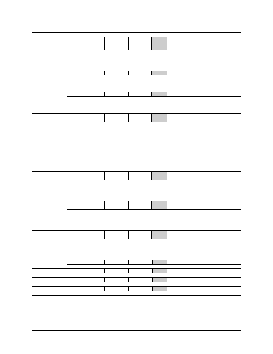
OZ998
OZ998-SF-2.2
Page
4
Name Pin
No.
Type
Input Drive
Definition
GPIO[7:3]/ID[7:3]
[17:15],
[13:12]
I/O TTL 12mA
General Purpose I/Os
Fully programmable GPIOs that can be used for a variety of dedicated or specific functions. GPIO[7:3] pins
default as inputs. They are programmable to function as GPI[7:3] inputs, GPO[7:3] outputs, ALF[7:3]
outputs, or ID[7:3] inputs. In addition, if this pin is configured as output, TTL output, Open Drain or Open
collector can be selected. Refer to GPIO Config.1&2 Registers for more details and GPIO Config. Tables
(section 8) for input/output selections.
GPIO[10:8]
[20:18] I/O
TTL
4mA
General Purpose I/Os
Fully programmable GPIOs that can be used for a variety of dedicated or specific functions. Pins
GPIO[10:8] default as inputs. Pins GPIO[10:8] as inputs are programmable to generate SMI/SMB
interrupts. They are also programmable to function as GPI[10:8] inputs, GPO[10:8] outputs. Refer to GPIO
Config.1&2 Registers for more details and GPIO Config. Tables (section 8) for input/output selections.
GPIO[11]
21 I/O TTL 4mA
General Purpose I/O
Fully programmable GPIO that can be used for a variety of dedicated or specific functions. Pin GPIO[11] is
default as input. Pin GPIO[11] as input is programmable to generate SMI/SMB interrupts. They are also
programmable to function as GPI[11] input, GPO[11] output. Refer to GPIO Config.1&2 Registers for more
details and GPIO Config. Tables (section 8) for input/output selections.
GPIO[12]/
SMB_SEL[0]
22 I/O TTL 4mA
General Purpose I/O /
Secondary SMBus Select 0
Fully programmable GPIO that can be used for a variety of dedicated or specific functions. By default,
GPIO[12] becomes SMB_SEL[0] input to be used to select Secondary SMBus. Pin GPIO[12] default as
input. Pin GPIO[12] as input is programmable to generate SMI/SMB interrupts. It is also programmable to
function as GPI[12] input, GPO[12] output. Refer to GPIO Config.1&2 Registers for more details and GPIO
Config. Tables (section 8) for input/output selections.
SMB_SEL[1:0] Selected Secondary SMBus
00 None
01 Secondary SMBus-1
10 Secondary SMBus-2
11 Secondary SMBus-3
GPIO[13]/
SMB_SEL[1]
23 I/O TTL 4mA
General Purpose I/O /
Secondary SMBus Select 1
Fully programmable GPIO that can be used for a variety of dedicated or specific functions. On default,
GPIO[13] becomes SMB_SEL[1] input to be used to select Secondary SMBus. Pin GPIO[13] default as
input. Pin GPIO[13], as input is programmable to generate SMI/SMB interrupts. It is also programmable to
function as GPI[13] input, GPO[13] output. Refer to GPIO Config.1&2 Registers for more details and GPIO
Config. Tables (section 8) for input/output selections.
GPIO[14]/
S_SMBDATA3
24 I/O TTL 4mA
General Purpose I/O /
Secondary SMBus-3 Data I/O
Fully programmable GPIO that can be used for a variety of dedicated or specific functions. Pin GPIO[14]
default as input. Pin GPIO[14], as input is programmable to generate SMI/SMB interrupts. It is also
programmable to function as GPI[14] input, GPO[14] outputs or secondary SMBus-3 Data Input/Output.
Refer to GPIO Config.1&2 Registers for more details and GPIO Config. Tables (section 8) for input/output
selections.
GPIO[15]/
S_SMBCLK3
25 I/O TTL 4mA
General Purpose I/O /
Secondary SMBus-3 Clock I/O
Fully programmable GPIO that can be used for a variety of dedicated or specific functions. Pin GPIO[15]
default as input. Pin GPIO[15], as input is programmable to generate SMI/SMB interrupts. It is also
programmable to function as GPI[15] input, GPO[15] output or secondary SMBus-3 Clock Input/Output.
Refer to GPIO Config.1&2 Registers for more details and GPIO Config. Tables (section 8) for input/output
selections.
XOUT
26 O
-
-
XOUT Output
Crystal output pin. See application diagram on p.18.
XIN/32KHZ
27 I TTL
-
XIN Input/32KHZ
32KHZ input clock source. Crystal input pin as alternate. See application diagram on p.18.
GND
14 GND
-
-
Ground
Ground.
VCC
28 PWR
-
-
3.3V/5V Power Supply
3.3V or 5V Power Supply.
OZ998
OZ998-SF-2.2
Page
5
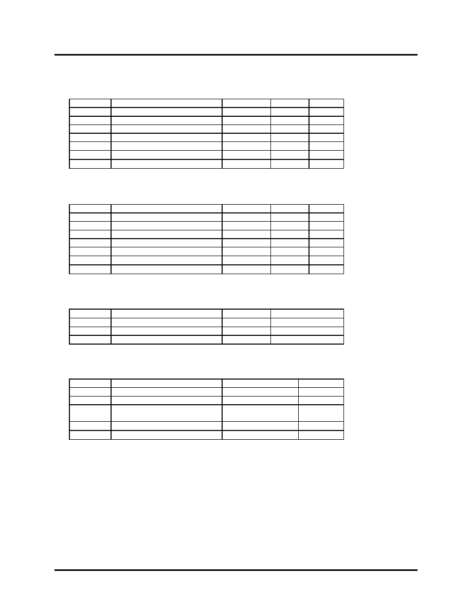
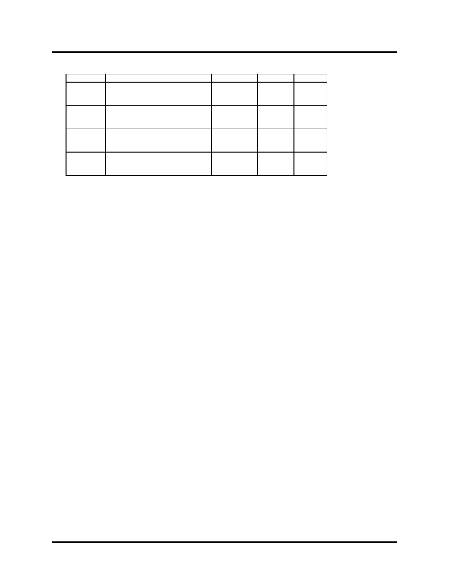
DC CHARACTERISTICS
DC TABLE FOR VCC = 5.0V
r
10%
Symbol
Parameter Min
Max
Units
V
CC
Power Supply Voltage
4.5
5.5
V
V
IH
Input HIGH Voltage
2.0
-
V
V
Il
Input LOW Voltage
-
0.8
V
V
OH
Output HIGH Voltage
2.4
-
V
V
OL
Output LOW Voltage
-
0.4
V
I
IL
Maximum Input Leakage Current
-10
10
µ
A
I
OL
Maximum Output Leakage
-10
10
µ
A
DC TABLE FOR VCC = 3.3V
r
10%
Symbol
Parameter Min
Max
Units
V
CC
Power Supply Voltage
3.0
3.6
V
V
IH
Input HIGH Voltage
2.0
-
V
V
Il
Input LOW Voltage
-
0.8
V
V
OH
Output HIGH Voltage
2.4
-
V
V
OL
Output LOW Voltage
-
0.4
V
I
IL
Maximum Input Leakage Current
-10
10
µ
A
I
OL
Maximum Output Leakage
-10
10
µ
A
CAPACITANCE
Symbol
Parameter
0
q
C to 70
q
C
Units
C
IN
Maximum Input Capacitance
10
pF
C
OUT
Maximum Output Capacitance
10
pF
C
IO
Maximum I/O Capacitance
10
pF
ABSOLUTE MAXIMUM RATINGS
Symbol
Parameter Value
Units
V
CC
DC Power Supply Voltage
-0.3 to 5.5
V
V
IN,
V
OUT
DC Input, Output Voltage
-0.3 to V
CC
+ 0.3
V
I
IN
DC Current Drain V
CC
and V
CC
Pins
±
25
mA
T
STG
Storage Temperature
-40 to +125
°
C
T
OPER|
Operation Temperature
0 to 70
°
C
OZ998
OZ998-SF-2.2
Page
6
I
CC
SPECIFICATIONS
Symbol Parameter
Typ
Max
Units
I
CC5V
Supply Current, V
CC
= 5V (when
32KHZ input clock source is
used)
8
15
µ
A
I
CC3V
Supply Current, V
CC
= 3.3V
(when 32KHZ input clock source
is used)
5
10
µ
A
I
CC5V
Supply Current, V
CC
= 5V (when
external OSC is used based on
configuration on p.18)
150 200
µ
A
I
CC3V
Supply Current, V
CC
= 3.3V
(when external OSC is used
based on configuration on p.18)
50
80
µ
A
OZ998
OZ998-SF-2.2
Page
7
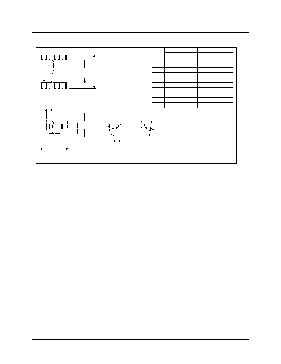
13. OZ998 PACKAGE INFORMATION
D
L
C
A
A1
D
B
e
E
H
SSOP
PACKAGE
(209 mil)
INCHES MILLIMETERS
DIM
MIN MAX MIN MAX
A 0.084
2.13
A1 0.002 0.010 0.05 0.25
B 0.009 0.015 0.22 0.38
C 0.004 0.008 0.09 0.20
D 0.390 0.413 9.90 10.50
E 0.197 0.220 5.00 5.60
e 0.0256
0.65
H 0.291 0.323 7.40 8.20
L 0.025
0.041 0.63 1.03
0
°
8
°
0
°
8
°
Document Outline