
Preliminary Information
T73327 / 73327A / 73327B
15-36 MHz, 3.3V VCXO
Applications
∑ Crystal-driven clock source for low cost set top boxes
General Description
The TLSI T73327/73327A is a single-chip, low-jitter Voltage-Controlled-Crystal-Oscillator. The device
accepts a 15 MHz-36 MHz crystal input and produces a low-jitter output at the same frequency. A 0V to
+3.3V control signal is used to fine-tune the output clock frequency in the ±120ppm range.
Features
∑ +3.3V operating voltage
∑ Uses inexpensive pullable crystals
∑ 12mA drive capability at TTL levels
∑ Low Cost
∑ 240 ppm pull range (±120 ppm)
∑ Excellent pull range linearity
∑ 8-pin SOIC, 8-pin MSOP packages available
∑ Alternate industry pinouts available
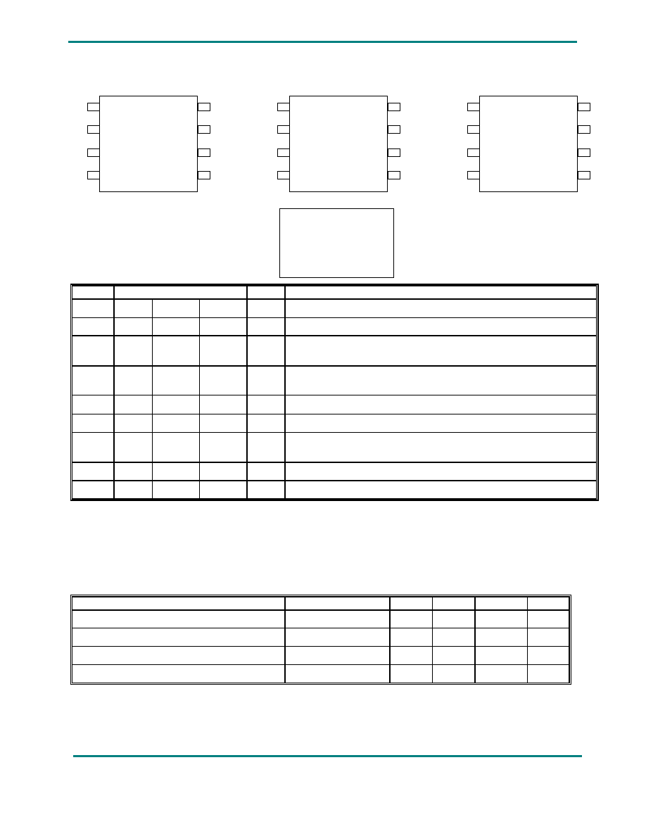
Figure 1. Functional Block Diagram
T73327/73327A/73327BPI Page
1
Rev J, January 14, 2005
TLSI Incorporated, 770 Park Avenue
, Huntington NY 11743 ∑ (631) 755-7005 ∑ Fax 631-755-7626 ∑ www.tlsi.com
VDD
CLK
X2
15 MHz ≠ 36MHz
Pullable Crystal
VIN
Output
Buffer
X1
Oscillator
GND
T73327/T73327A/T73327B
Preliminary Information
T73327/73327A/73327BPI
Page
2
Rev J, January 14, 2005
Figure 2. Pin Configuration
8-pin SOIC/MSOP
8-pin SOIC/MSOP
8-pin SOIC/MSOP
X1
X2
X1
X2
X1
X2
1
8
1
8
1
8
NC
NC
GND
V
DD
**
NC
V
DD
2
7
2
7
2
7
T73327A
T73327B
T73327
V
DD
CLK
V
IN
NC**
V
IN
V
IN
3
6
3
6
3
6
GND
GND
GND
CLK
CLK
NC
4
5
4
5
4
5
8-pin SOIC/MSOP
(See pages 4 & 5
for package outlines
&
ordering information)
Table 1. Pin Description
Name Pin
No. Type
Description
73327 73327A 73327B
X1
1
1
1
Xi
Crystal connection. Connect to a 15 MHz - 36MHz pullable crystal
V
DD
**
2** 6 2 P
This pin can alternately be used to connect
V
DD
instead of pin 6 or left
unconnected (for T73327 only).
V
IN
3
3
3
I
Tuning control input. Zero to +3.3V signal controls the frequency of the
VCXO.
GND
4, 7
4
4
P
Connect to ground.
CLK
5
5
6
O
Clock output
NC** 6** -
5 NC
This pin can alternately be used to connect
V
DD
instead of pin 2 or left
unconnected (for T73327 only).
NC
-
2, 7
7
NC
Do not connect
X2
8
8
8
Xi
Crystal connection. Connect to a 15 MHz ≠ 36 MHz pullable crystal.
Legend:
I = Input
Xi = Crystal connections
O = Output
NC = No connection
P = Power supply connection
**Note:
On the T73327 only, both pin 2 and pin 6 are internally connected to V
DD
. Either pin or both can safely be connected to
V
DD
without damaging the part. Alternately, at the user's option, one pin may be used for V
DD
with the other pin being left
unconnected (NC).
Table 2. Absolute Maximum Ratings
Parameter Conditions
Min
Typ
Max
Units
Supply voltage, V
DD
Referenced to GND
7
V
Inputs and Clock Outputs
Referenced to GND
-0.5
VDD+0.5
V
Soldering Temperature
Max of 10 seconds
+260
∞C
Storage temperature
-65
+150
∞C
Stresses above those listed under Absolute Maximum Ratings may cause permanent damage to the device. These
ratings are stress specifications only and correct functional operation of the device at these or any other conditions
above those listed in the operational sections of the specifications is not implied. Exposure to absolute maximum rating
conditions for extended periods may affect product reliability.
TLSI Incorporated, 770 Park Avenue
, Huntington NY 11743 ∑ (631) 755-7005 ∑ Fax 631-755-7626 ∑ www.tlsi.com

T73327/T73327A/T73327B
Preliminary Information
T73327/73327A/73327BPI Page
3
Rev J, January 14, 2005
Table 3. Operating Conditions
Parameter Conditions
Min
Typ
Max
Units
Operating Voltage, V
DD
+3.135
+3.3
+3.465
V
Input High Voltage, V
IH
, X1 pin only
+2.5
V
Input Low Voltage, V
IL
, X1 pin only
+0.4
V
Operating Temperature
0
+70
∞C
VCXO control voltage, V
IN
0
+3.3
V
Table 4. DC Electrical Characteristics
T
A
= 0
∞C to +70∞C, V
DD
= +3.135 V to +3.465 V
Parameter Condition
Min
Typ
(1)
Max Units
Output High Voltage, V
OH
I
OH
= -12mA
2.4
V
Output Low Voltage, V
OL
I
OL
= 12mA
0.4
V
Operating Supply Current, I
DD
No Load, 27 MHz
14.0
20.0
mA
Short Circuit Current
Each output
±50
mA
Input Capacitance
7
pF
Note:
1. Typical values are at V
DD
= 3.3V and +25∞C
Table 5. AC Electrical Characteristics
T
A
= 0
∞C to +70∞C, V
DD
= +3.135 V to +3.465 V
Symbol Parameter
Condition
Min
Typ
(1)
Max Units
fosc
Input Crystal Frequency
15
27
36
MHz
tr
Output Clock Rise Time
+0.8 to +2.0V
1.5
ns
tf
Output Clock Fall Time
+2.0 to +0.8V
1.5
ns
t
od
Output Clock Duty Cycle
At V
DD
/2 45
50
55
%
Lin
Pull Range Linearity
(2)
V
IN
= 0.1 V
DD
~ 0.9 V
DD
5 %
Frequency vs Supply voltage
5
%
t
jit
(pk ≠ pk)
Maximum Absolute Jitter
(Peak to Peak)
C
L
= 15pF
50
ps
Phase Noise
27 MHz @ 10 KHz
27 MHz @ 100 KHz
-154
-156
dBc/Hz
dBc/Hz
f
PULL
Output frequency pullability
0V
V
IN
+3.3V
±100 ±120
ppm
Note:
1.
Typical values are at V
DD
= +3.3V and +25∞C
2.
Mil-PRF-55310D 4.8.31.5 Deviation Linearity
TLSI Incorporated, 770 Park Avenue
, Huntington NY 11743 ∑ (631) 755-7005 ∑ Fax 631-755-7626 ∑ www.tlsi.com

T73327/T73327A/T73327B
Preliminary Information
T73327/73327A/73327BPI Page
4
Rev J, January 14, 2005
Table 6. Pullable Crystal Specifications
Parameter Symbol
Value
Correlation (Load) Capacitance
C
L
18 pF (typ)
Capacitance Ratio
C
O
/C
1
240
max
Equivalent Series Resistance
ESR
30
max
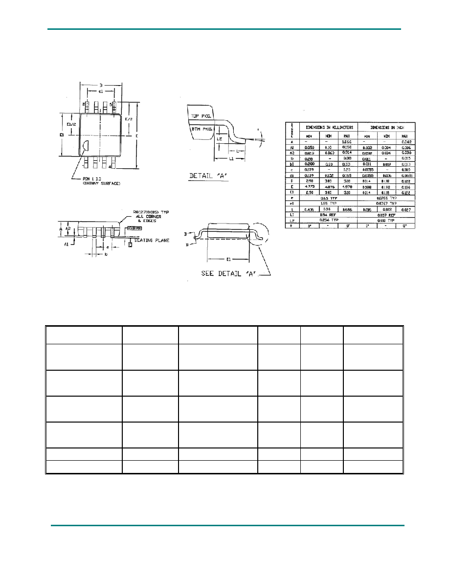
Figure 3. Package Outline (8-pin SOIC)
TLSI Incorporated, 770 Park Avenue
, Huntington NY 11743 ∑ (631) 755-7005 ∑ Fax 631-755-7626 ∑ www.tlsi.com
T73327/T73327A/T73327B
Preliminary Information
T73327/73327A/73327BPI Page
5
Rev J, January 14, 2005
Figure 4. Package Outline (8-pin MSOP)
Table 7. Ordering Information
Part Number
Marking
Shipping/Packaging
No. of
Pins
Package
Temperature
T73327-SO8
T73327A-SO8
T73327B-SO8
T73327
T73327A
T73327B
Tubes 8
SOIC
0
∞C to +70∞C
T73327-SO8-TNR
T73327A-SO8-TNR
T73327B-SO8-TNR
T73327
T73327A
T73327B
Tape & Reel
8
SOIC
0
∞C to +70∞C
T73327-MO8
T73327A-MO8
T73327B-MO8
T73327
T73327A
T73327B
Tubes 8
MSOP
0
∞C to +70∞C
T73327-MO8-TNR
T73327A-MO8-TNR
T73327B-MO8-TNR
T73327
T73327A
T73327B
Tape & Reel
8
MSOP
0
∞C to +70∞C
T73327-DIE
N/A
Die in Waffle Pack
8
N/A
0
∞C to +70∞C
T73327-DPW
N/A
Die in Probed Wafer
8
N/A
0
∞C to +70∞C
TLSI Incorporated, 770 Park Avenue
, Huntington NY 11743 ∑ (631) 755-7005 ∑ Fax 631-755-7626 ∑ www.tlsi.com