 | –≠–ª–µ–∫—Ç—Ä–æ–Ω–Ω—ã–π –∫–æ–º–ø–æ–Ω–µ–Ω—Ç: T73LVP22 | –°–∫–∞—á–∞—Ç—å:  PDF PDF  ZIP ZIP |
Preliminary Information
T73LVP22
Dual 3.3V LVTTL/LVCMOS-to-Differential
LVPECL Translator
Applications
∑ Multiple LVPECL clock sources
General Description
The TLSI T73LVP22 is a general-purpose dual LVTTL (LVCMOS)-to-differential LVPECL translator
operating from a single +3.3V supply. The device has two independent channels that accept an LVTTL or
LVCMOS input and provide differential LVPECL outputs referenced to the positive supply rail. The small 8-
pin SOIC package makes it ideal for applications which require the translation of multiple clocks or data
signals, and where cost, performance and size are of critical importance. The T73LVP22 is 100K PECL
compatible and is a pin-for-pin replacement for the MC100EPT22D.
Features
∑ 350pS typical propagation delay
∑ Operating Frequency > 1 GHz
∑ Differential LVPECL outputs
∑ Flow-through pinout
∑ Q, Q1 outputs default low with input
(D) open
∑ ESD rating >2000V (Human Body
Model) or >200V (Machine Model)
∑ -40
o
C to +85
o
C operating temperature
range
∑ Available in standard 8-pin SOIC
package
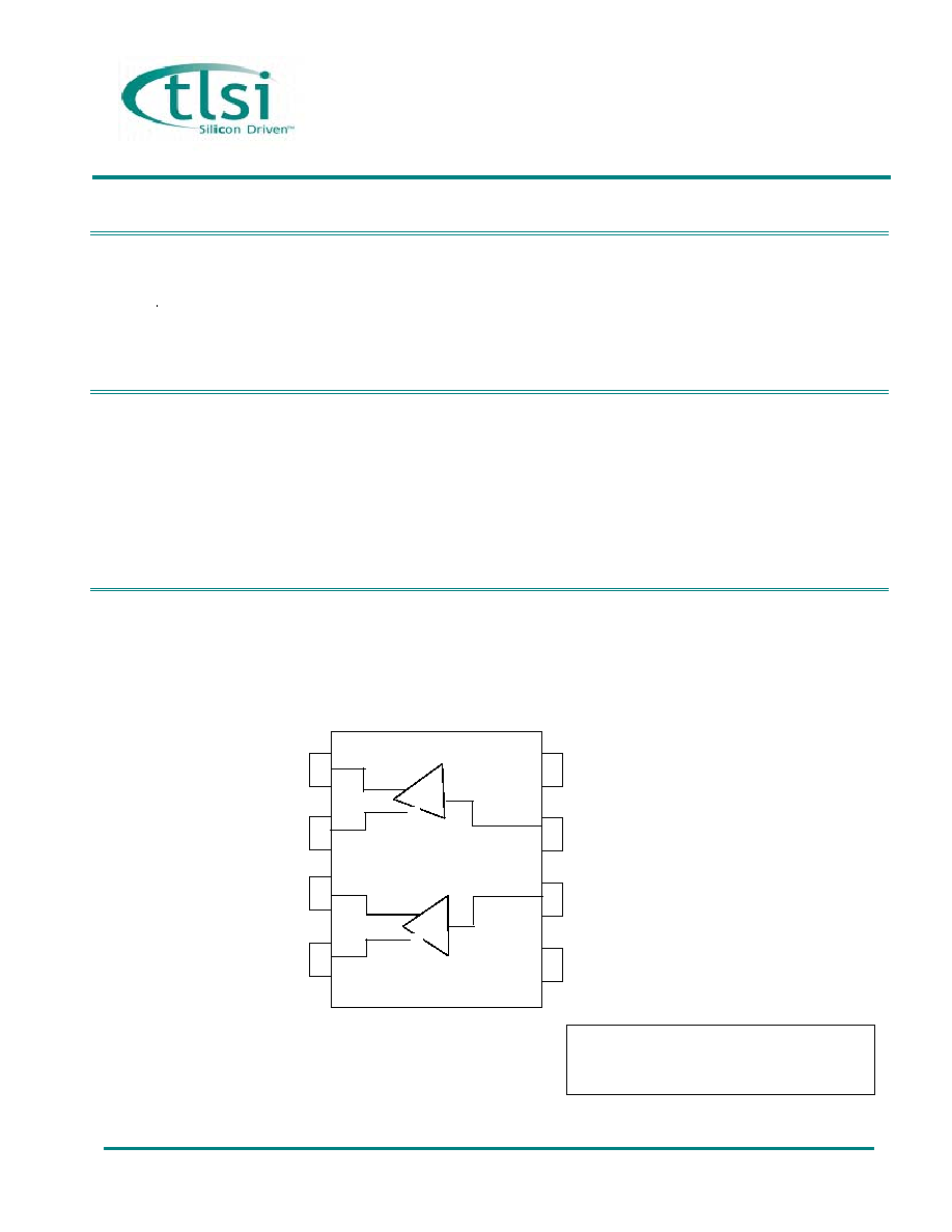
Figure 1. Functional Block Diagrams & Pin Assignments (Top View)
8-pin SOIC
4
1
2
3
6
7
8
5
Q
V
DD
LVTTL/
LVCMOS
LVPECL
Q
n
D
Q1
D1
LVTTL/
LVCMOS
LVPECL
Q1
n
GND
See page 4 for package outline drawing
and
ordering information.
T73LVP22PI Page
1
Rev A February 23, 2004
TLSI Incorporated, 770 Park Avenue
, Huntington NY 11743 ∑ (631) 755-7005 ∑ Fax 631-755-7626 ∑ www.tlsi.com
T73LVP22 Preliminary Information
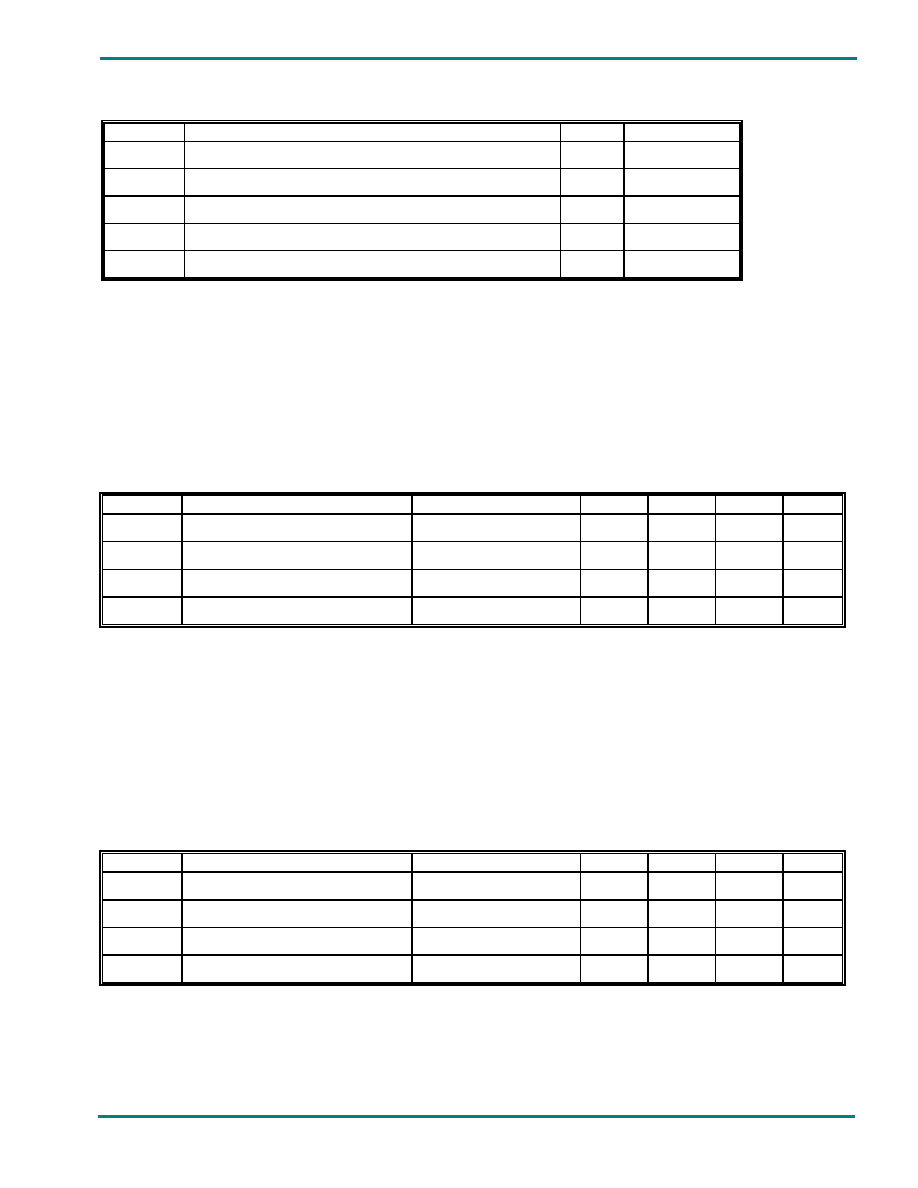
Table 1. Pin Description
Name Description Type
Pin
#
Q, Q1
LVPECL data outputs
O
1, 3
Q
n
, Q1
n
LVPECL complementary data outputs
O
2, 4
V
DD
Connect to +3.3V
P
8
D, D1
LVCMOS/LVTTL data inputs
I
7, 6
GND
Connect to ground
P
5
Legend: I = Input
O = Output
P = Power supply connection
Table 2. Absolute Maximum Ratings (each channel)
Symbol Parameter
Conditions
Min
Typ
Max
Units
V
DD
Supply voltage
Referenced to GND
+5.0
V
V
IN
Input voltage
Referenced to GND
-0.5
V
DD
V
I
OUT
Output current
Continuous
50
mA
T
STG
Storage
temperature
-65 +150
o
C
Stresses above those listed under Absolute Maximum Ratings may cause permanent damage to the device. These ratings are stress
specifications only and correct functional operation of the device at these or any other conditions above those listed in the operational
sections of the specifications is not implied. Exposure to absolute maximum rating conditions for extended periods may affect product
reliability.
Table 3. Operating Conditions (each channel)
Symbol Parameter
Conditions
Min
Typ
Max
Units
V
DD
Power Supply Voltage
+3.0
+3.3
+3.6
V
T
A
Ambient
Temperature
-40
+85
o
C
V
IH
Input HIGH Voltage
+2.0
V
V
IL
Input LOW Voltage
+0.8
V
T73LVP22PI Page
2
Rev A February 23, 2004
TLSI Incorporated, 770 Park Avenue
, Huntington NY 11743 ∑ (631) 755-7005 ∑ Fax 631-755-7626 ∑ www.tlsi.com

T73LVP22 Preliminary Information
Table 4. DC Characteristics (each channel)
T
A
= -40
o
C to +85
o
C, V
DD
= +3.0V to +3.6V unless otherwise stated below.
Symbol Parameter
Conditions Min
Typ
Max
Units
I
IH
Input HIGH Current
V
IN
=+2.7V
100
µA
I
IL
Input LOW Current
V
IN
= +0.5V
1
µA
V
IK
Input Clamp Diode Voltage
I
IN
= -18mA
-1.2
V
-40
o
C 2220
2320
2420
mV
+25
o
C 2220
2320
2420
mV
V
OH
Output HIGH Voltage
(1, 2)
+85
o
C
V
DD
= +3.3V
2220 2320 2420 mV
-40
o
C 1420
1520
1620
mV
+25
o
C 1420
1520
1620
mV
V
OL
Output LOW Voltage
(1, 2)
+85
o
C
V
DD
= +3.3V
1420 1520 1620 mV
I
DD
Power Supply Current
Total both channels, no load
46
mA
Notes:
1. The T73LVP22 is designed to meet these specifications after thermal equilibrium has been established.
The circuit is in a test socket or mounted on a printed circuit board.
2. Q, Q1 and Qn, Q1n outputs are loaded with 50 ohms to V
DD
-2 volts.
Table 5. AC Characteristics (each channel)
T
A
= -40
o
C to +85
o
C, V
DD
= +3.0V to +3.6V
Symbol Parameter
Conditions
Min
Typ
Max
Units
t
PLH
Propagation
Delay
(1)
To Output Differential
350
500
ps
t
PHL
Propagation
Delay
(1)
To Output Differential
350
500
ps
t
r
/t
f
Output Rise/Fall time
20%-80%, Q/Q
n
80 130 200 ps
f
MAX
Maximum Input Frequency
LVTTL or LVCMOS
input
>
1 GHz
f
MAX
Maximum Input Frequency
(2)
750mV
peak-to-peak
sine wave centered
around 1.5V
>
1 GHz
Notes:
1. Q, Q1 and Qn, Q1n outputs are loaded with 50 ohms to V
DD
-2 volts.
2. Measured using a 750mV peak-to-peak, 50% duty cycle clock source.
T73LVP22PI Page
3
Rev A February 23, 2004
TLSI Incorporated, 770 Park Avenue
, Huntington NY 11743 ∑ (631) 755-7005 ∑ Fax 631-755-7626 ∑ www.tlsi.com
T73LVP22 Preliminary Information
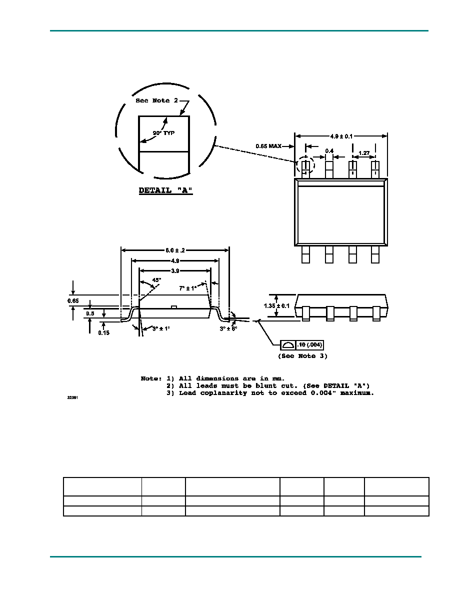
Figure 2. Package Outline (8-pin SOIC)
Table 6. Ordering Information
Part Number
Marking
Shipping/Packaging
No. of
Pins
Package
Temperature
T73LVP22-S08 T73LVP22
Tubes
8 SOIC
-40
∞C to +85∞C
T73LVP22-S08-TNR T73LVP22
Tape & Reel
8
SOIC
-40
∞C to +85∞C
T73LVP22PI Page
4
Rev A February 23, 2004
TLSI Incorporated, 770 Park Avenue
, Huntington NY 11743 ∑ (631) 755-7005 ∑ Fax 631-755-7626 ∑ www.tlsi.com