
1
V55C2256164VB
256Mbit MOBILE SDRAM
2.5 VOLT FBGA PACKAGE 16M X 16
V55C2256164VB Rev. 1.0 April 2005
7
8PC
10
System Frequency (f
CK
)
143 MHz
125 MHz
100MHz
Clock Cycle Time (t
CK3
)
7 ns
8 ns
10 ns
Clock Access Time (t
AC3
) CAS Latency = 3
5.4 ns
6 ns
7 ns
Clock Access Time (t
AC2
) CAS Latency = 2
6 ns
6 ns
8 ns
Clock Access Time (t
AC1
) CAS Latency = 1
19 ns
19 ns
22 ns
Features
4 banks x 4Mbit x 16 organization
High speed data transfer rates up to 143 MHz
Full Synchronous Dynamic RAM, with all signals
referenced to clock rising edge
Single Pulsed RAS Interface
Data Mask for Read/Write Control
Four Banks controlled by BA0 & BA1
Programmable CAS Latency:1, 2, 3
Programmable Wrap Sequence: Sequential or
Interleave
Programmable Burst Length:
1, 2, 4, 8, Full page for Sequential Type
1, 2, 4, 8 for Interleave Type
Multiple Burst Read with Single Write Operation
Automatic and Controlled Precharge Command
Random Column Address every CLK (1-N Rule)
Power Down Mode and Clock Suspend Mode
Deep Power Mode
Auto Refresh and Self Refresh
Refresh Interval: 8192 cycles/64 ms
Available in 54-ball FBGA, with 9x6 ball array
with 3 depupulated rows, 13x8 mm and 54 pin
TSOP II
VDD=2.5V, VDDQ=1.8V
Programmable Power Reduction Feature by par-
tial array activation during Self-Refresh
Operating Temperature Range
Commercial (
0
∞
C to 70
∞
C)
Industrial
(-40
∞
C to +85
∞
C)
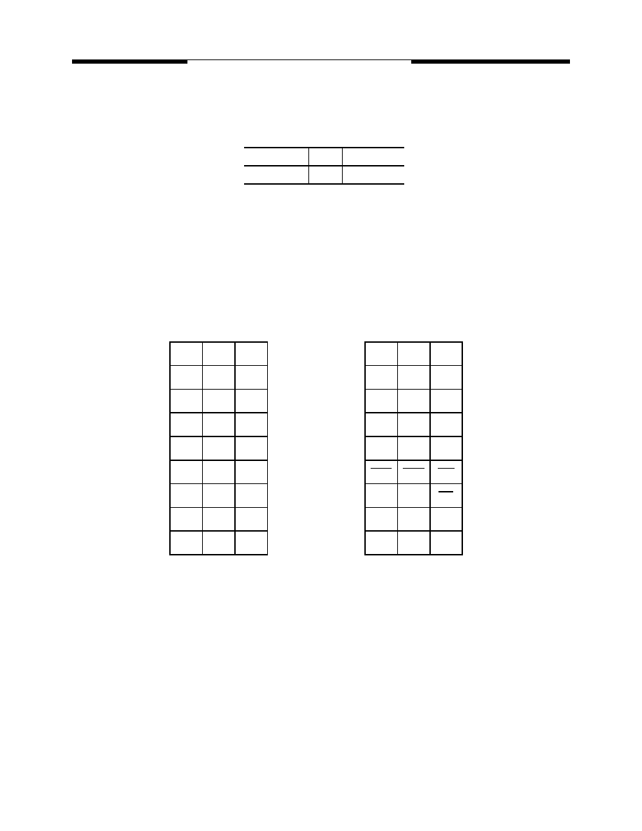
Device Usage Chart
Operating
Temperature
Range
Package Outline
Access Time (ns)
Temperature
Mark
C/T
7
8PC
10
0
∞
C to 70
∞
C
∑
∑
∑
∑
Commercial
-40
∞
C to 85
∞
C
∑
∑
∑
∑
Extended

2
V55C2256164VB Rev. 1.0 April 2005
ProMOS TECHNOLOGIES
V55C2256164VB
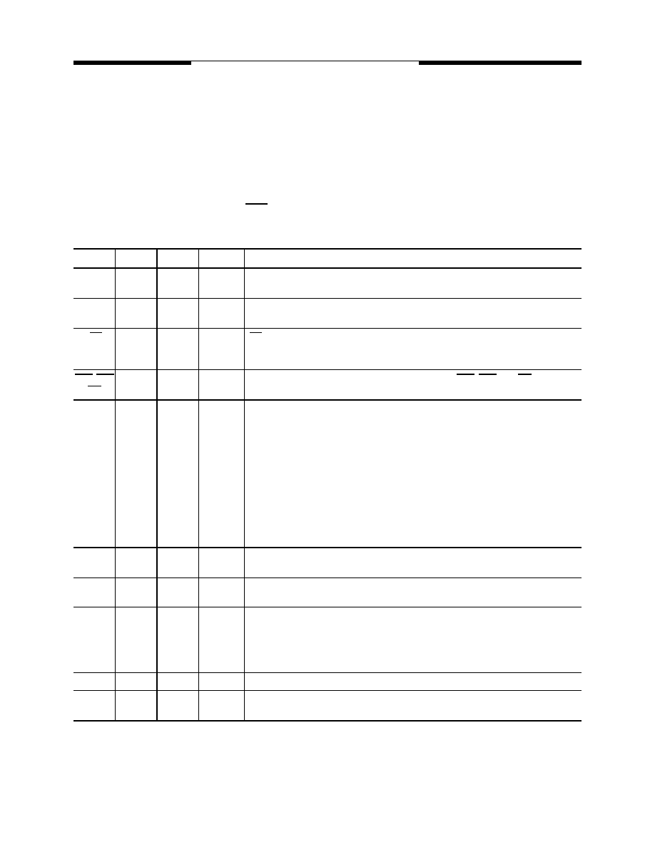
Part Number Information
V
5 5
C
2
2 5 6 1 6
4
V
T
7
ORGANIZATION
ProMOS
& REFRESH
OTHER
PC
: CL2
TYPE
16Mx16, 8K : 25616
BLANK: CL3
53 DRAM
54
SDRAM
TEMPERATURE
55
MOBILE SDRAM
BLNK: 0 - 70C
I :
-40 - 85C
E :
-40 - 125C
CMOS
BANKS
SPEED
VOLTAGE
2 : 2 BANKS
I/O
10 :
100MHz
7 : 143MHz
3 : 3.3 V
4 : 4 BANKS
V: LVTTL
8 : 125MHz
: 6 : 166MHz
2 :
2.5 V
8 : 8 BANKS
75
: 133MHz
5 : 200MHz
1 : 1.8 V
REV LEVEL
A: 1st C: 3rd
PACKAGE
B: 2nd D: 4th
LEAD PLATING
LEAD FREE
GREEN
PACKAGE DESC.
TSOP
SPECIAL FEATURE
60-Ball FBGA
L: STANDARD LOW POWER
54-Ball FBGA
U: ULTRA LOW POWER
BGA
Die-Stacked TSOP
Die-Stacked FBGA
TI
SI
E
F
G
H
TE
SF
I
J
K
M
TS
SS
T
S
C
B
B
3
V55C2256164VB Rev.1.0 April 2005
ProMOS TECHNOLOGIES
V55C2256164VB
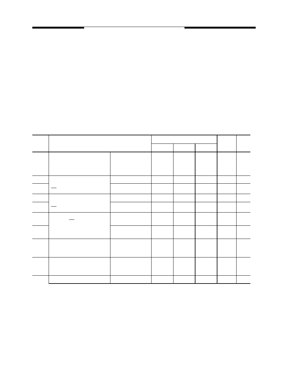
60 Pin WBGA PIN CONFIGURATION
Top View
Description
Pkg.
Pin Count
FBGA
C
54
Pin Configuration for x16 devices:
< Top-view >
1
2
3
7
8
9
VSS DQ15 VSSQ
A
VDDQ DQ0
VDD
DQ14 DQ13 VDDQ
B
VSSQ DQ2
DQ1
DQ12 DQ11 VSSQ
C
VDDQ DQ4
DQ3
DQ10 DQ9 VDDQ
D
VSSQ DQ6
DQ5
DQ8
NC
VSS
E
VDD LDQM DQ7
UDQM CLK
CKE
F
CAS
RAS
WE
A12
A11
A9
G
BA0
BA1
CS
A8
A7
A6
H
A0
A1
A10
VSS
A5
A4
J
A3
A2
VDD

4
V55C2256164VB Rev. 1.0 April 2005
ProMOS TECHNOLOGIES
V55C2256164VB
54 Pin Plastic TSOP-II
PIN CONFIGURATION
Top View
Pin Names
CLK
Clock Input
CKE
Clock Enable
CS
Chip Select
RAS
Row Address Strobe
CAS
Column Address Strobe
WE
Write Enable
A
0
≠A
12
Address Inputs
BA0, BA1
Bank Select
I/O
1
≠I/O
16
Data Input/Output
LDQM, UDQM
Data Mask
V
CC
Power (+3.3V)
V
SS
Ground
V
CCQ
Power for I/O's (+3.3V)
V
SSQ
Ground for I/O's
NC
Not connected
Description
Pkg.
Pin Count
TSOP-II
T
54
V
CC
I/O
1
V
CCQ
NC
I/O
2
V
SSQ
NC
I/O
3
V
CCQ
NC
I/O
4
V
SSQ
NC
V
CC
NC
WE
CAS
RAS
CS
BA0
BA1
A
10
A
0
A
1
A
2
A
3
V
CC
V
SS
I/O
8
V
SSQ
NC
I/O
7
V
CCQ
NC
I/O
6
V
SSQ
NC
I/O
5
V
CCQ
NC
V
SS
NC
DQM
CLK
CKE
A
12
A
11
A
9
A
8
A
7
A
6
A
5
A
4
V
SS
1
2
3
4
5
6
7
8
9
10
11
12
13
14
15
16
17
18
19
20
21
22
23
24
25
26
27
54
53
52
51
50
49
48
47
46
45
44
43
42
41
40
39
38
37
36
35
34
33
32
31
30
29
28
356804V-01
5
V55C2256164VB Rev. 1.0 April 2005
ProMOS TECHNOLOGIES
V55C2256164VB
Description
The V55C2256164VB is a four bank Synchronous DRAM organized as 4 banks x 4Mbit x 16. The
V55C2256164VB achieves high speed data transfer rates up to 143 MHz by employing a chip architecture
that prefetches multiple bits and then synchronizes the output data to a system clock.
All of the control, address, data input and output circuits are synchronized with the positive edge of an ex-
ternally supplied clock.
Operating the four memory banks in an interleaved fashion allows random access operation to occur at
higher rate than is possible with standard DRAMs. A sequential and gapless data rate of up to 143 MHz is
possible depending on burst length, CAS latency and speed grade of the device.
Signal Pin Description
Pin
Type
Signal
Polarity
Function
CLK
Input
Pulse
Positive
Edge
The system clock input. All of the SDRAM inputs are sampled on the rising edge of the
clock.
CKE
Input
Level
Active High Activates the CLK signal when high and deactivates the CLK signal when low, thereby
initiates either the Power Down mode or the Self Refresh mode.
CS
Input
Pulse
Active Low CS enables the command decoder when low and disables the command decoder when
high. When the command decoder is disabled, new commands are ignored but previous
operations continue.
RAS, CAS
WE
Input
Pulse
Active Low When sampled at the positive rising edge of the clock, CAS, RAS, and WE define the
command to be executed by the SDRAM.
A0 - A12
Input
Level
--
During a Bank Activate command cycle, A0-A12 defines the row address (RA0-RA12)
when sampled at the rising clock edge.
During a Read or Write command cycle, A0-An defines the column address (CA0-CAn)
when sampled at the rising clock edge.CAn depends from the SDRAM organization:
∑ 8M x 16 SDRAM CA0≠CA8.
In addition to the column address, A10(=AP) is used to invoke autoprecharge operation
at the end of the burst read or write cycle. If A10 is high, autoprecharge is selected and
BA0, BA1 defines the bank to be precharged. If A10 is low, autoprecharge is disabled.
During a Precharge command cycle, A10(=AP) is used in conjunction with BA0 and BA1
to control which bank(s) to precharge. If A10 is high, all four banks will BA0 and BA1 are
used to define which bank to precharge.
BA0,
BA1
Input
Level
--
Selects which bank is to be active.
DQx
Input
Output
Level
--
Data Input/Output pins operate in the same manner as on conventional DRAMs.
LDQM
UDQM
Input
Pulse
Active High The Data Input/Output mask places the DQ buffers in a high impedance state when sam-
pled high. In Read mode, DQM has a latency of two clock cycles and controls the output
buffers like an output enable. In Write mode, DQM has a latency of zero and operates as
a word mask by allowing input data to be written if it is low but blocks the write operation
if DQM is high.
VCC, VSS
Supply
Power and ground for the input buffers and the core logic.
VCCQ
VSSQ
Supply
--
--
Isolated power supply and ground for the output buffers to provide improved noise
immunity.

6
V55C2256164VB Rev. 1.0 April 2005
ProMOS TECHNOLOGIES
V55C2256164VB
Operation Definition
All of SDRAM operations are defined by states of control signals CS, RAS, CAS, WE, and DQM at the
positive edge of the clock. The following list shows the thruth table for the operation commands.
Notes:
1.
V = Valid , x = Don't Care, L = Low Level, H = High Level
2.
CKEn signal is input level when commands are provided, CKEn-1 signal is input level one clock before the commands
are provided.
3.
These are state of bank designated by BS0, BS1 signals.
4.
Power Down Mode can not entry in the burst cycle.
5. After Deep Power Down mode exit a full new initialization of memory device is mandatory
Operation
Device
State
CKE
n-1
CKE
n
CS
RAS
CAS
WE
DQM
A0-9,
A11
A10
BS0
BS1
Row Activate
Idle
3
H
X
L
L
H
H
X
V
V
V
Read
Active
3
H
X
L
H
L
H
X
V
L
V
Read w/Autoprecharge
Active
3
H
X
L
H
L
H
X
V
H
V
Write Active
3
H
X
L
H
L
L
X
V
L
V
Write with Autoprecharge
Active
3
H
X
L
H
L
L
X
V
H
V
Row Precharge
Any
H
X
L
L
H
L
X
X
L
V
Precharge All
Any
H
X
L
L
H
L
X
X
H
X
Mode Register Set
Idle
H
X
L
L
L
L
X
V
V
V
No Operation
Any
H
X
L
H
H
H
X
X
X
X
Device Deselect
Any
H
X
H
X
X
X
X
X
X
X
Auto Refresh
Idle
H
H
L
L
L
H
X
X
X
X
Self Refresh Entry
Idle
H
L
L
L
L
H
X
X
X
X
Self Refresh Exit
Idle
(Self Refr.)
L
H
H
X
X
X
X
X
X
X
L
H
H
X
Power Down Entry
Idle
Active
4
H
L
H
X
X
X
X
X
X
X
L
H
H
X
Power Down Exit
Any
(Power
Down)
L
H
H
X
X
X
X
X
X
X
L
H
H
L
Data Write/Output Enable
Active
H
X
X
X
X
X
L
X
X
X
Data Write/Output Disable
Active
H
X
X
X
X
X
H
X
X
X
Deep Pwoer Down Entry
Idle
H
L
L
H
H
L
H
X
X
X
Deep Pwoer Down Exit
Deep power-
Down
L
H
X
X
X
X
H
X
X
X

7
V55C2256164VB Rev.1.0 April 2005
ProMOS TECHNOLOGIES
V55C2256164VB
Power On and Initialization
The default power on state of the mode register is
supplier specific and may be undefined. The
following power on and initialization sequence
guarantees the device is preconditioned to each
users specific needs. Like a conventional DRAM,
the Synchronous DRAM must be powered up and
initialized in a predefined manner. During power on,
all VCC and VCCQ pins must be built up
simultaneously to the specified voltage when the
input signals are held in the "NOP" state. The power
on voltage must not exceed VCC+0.3V on any of
the input pins or VCC supplies. The CLK signal
must be started at the same time. After power on,
an initial pause of 200
µ
s is required followed by a
precharge of both banks using the precharge
command. To prevent data contention on the DQ
bus during power on, it is required that the DQM and
CKE pins be held high during the initial pause
period. Once all banks have been precharged, the
Mode Register and Low Power Mode Register Set
Command must be issued to initialize the Mode
Register. A minimum of two Auto Refresh cycles
(CBR) are also required.These may be done before
or after programming the Mode Register. Failure to
follow these steps may lead to unpredictable start-
up modes.
Programming the Mode Register
The Mode register designates the operation
mode at the read or write cycle. This register is di-
vided into 4 fields. A Burst Length Field to set the
length of the burst, an Addressing Selection bit to
program the column access sequence in a burst cy-
cle (interleaved or sequential), a CAS Latency Field
to set the access time at clock cycle and a Opera-
tion mode field to differentiate between normal op-
eration (Burst read and burst Write) and a special
Burst Read and Single Write mode. The mode set
operation must be done before any activate com-
mand after the initial power up. Any content of the
mode register can be altered by re-executing the
mode set command. All banks must be in pre-
charged state and CKE must be high at least one
clock before the mode set operation. After the mode
register is set, a Standby or NOP command is re-
quired. Low signals of RAS, CAS, and WE at the
positive edge of the clock activate the mode set op-
eration. Address input data at this timing defines pa-
rameters to be set as shown in the previous table.
Low Power Mode Register
The Low Power Mode Register controls functions
beyond those controlled by the Mode Register.
These additional functions are unique to the Low-
Power DRM and includes a Refresh Period field
(TCR) for temperature compensated self-refresh
and a Partial-Array Self-Refresh field (PAS). The
PASR field is used to specify whether only one
quarter (bank 0), one half (bank 0+1) or all banks of
the SDRAM array are enabled. Disabled banks will
not be refreshed in Self-Refresh mode and written
data will be lost. When only bank 0 is selected, it's
possible to partially select only half or mone quarter
of bank 0. The TCR field has four entries to set Re-
fresh Period during self-refresh depending on the
case temperature of the Low power RAM. It's re-
quired during the initialization seuqence and can be
modified when the part id idle.
Read and Write Operation
When RAS is low and both CAS and WE are high
at the positive edge of the clock, a RAS cycle starts.
According to address data, a word line of the select-
ed bank is activated and all of sense amplifiers as-
sociated to the wordline are set. A CAS cycle is
triggered by setting RAS high and CAS low at a
clock timing after a necessary delay, t
RCD
, from the
RAS timing. WE is used to define either a read
(WE = H) or a write (WE = L) at this stage.
SDRAM provides a wide variety of fast access
modes. In a single CAS cycle, serial data read or
write operations are allowed at up to a 125 MHz
data rate. The numbers of serial data bits are the
burst length programmed at the mode set operation,
i.e., one of 1, 2, 4, 8. Column addresses are seg-
mented by the burst length and serial data accesses
are done within this boundary. The first column ad-
dress to be accessed is supplied at the CAS timing
and the subsequent addresses are generated auto-
matically by the programmed burst length and its
sequence. For example, in a burst length of 8 with
interleave sequence, if the first address is `2', then
the rest of the burst sequence is 3, 0, 1, 6, 7, 4, and
5.

ProMOS TECHNOLOGIES
V55C2256164VB
8
V55C2256164VB Rev. 1.0 April 2005
Address Input for Mode Set (Mode Register Operation)
Similar to the page mode of conventional
DRAM's, burst read or write accesses on any col-
umn address are possible once the RAS cycle
latches the sense amplifiers. The maximum t
RAS
or
the refresh interval time limits the number of random
column accesses. A new burst access can be done
even before the previous burst ends. The interrupt
operation at every clock cycles is supported. When
the previous burst is interrupted, the remaining ad-
dresses are overridden by the new address with the
full burst length. An interrupt which accompanies
with an operation change from a read to a write is
possible by exploiting DQM to avoid bus contention.
When two or more banks are activated
sequentially, interleaved bank read or write
operations are possible. With the programmed
burst length, alternate access and precharge
operations on two or more banks can realize fast
serial data access modes among many different
pages. Once two or more banks are activated,
column to column interleave operation can be done
between different pages.
A12 ...
A3
A4
A2
A1
A0
A7
A6
A5
Address Bus (Ax)
BT
Burst Length
CAS Latency
Mode Register
CAS Latency
A6
A5
A4
Latency
0
0
0
Reserve
0
0
1
1
0
1
0
2
0
1
1
3
1
0
0
Reserve
1
0
1
Reserve
1
1
0
Reserve
1
1
1
Reserve
Burst Length
A2
A1
A0
Length
Sequential
Interleave
0
0
0
1
1
0
0
1
2
2
0
1
0
4
4
0
1
1
8
8
1
0
0
Reserve
Reserve
1
0
1
Reserve
Reserve
1
1
0
Reserve
Reserve
1
1
1
Full page
Reserve
Burst
Type
A3
Type
0
Sequential
1
Interleave
Operation Mode
BA1 BA0 A12 A11 A10 A9 A8 A7
Mode
0
0
0
0
0
0
0
0
Burst Read/Burst
Write
0
0
0
0
0
1
0
0
Burst Read/Single
Write
Operation Mode
BA0
BA1

9
V55C2256164VB Rev. 1.0 April 2005
ProMOS TECHNOLOGIES
V55C2256164VB
A12 to A5
A3
A4
A2
A1
A0
Address Bus (Ax)
TCR
PASR
Mode Register
A4
A3
Max case temp
0
0
70
O
C
0
1
45
O
C
1
0
15
O
C
1
1
85
O
C
all have to be set to "0"
BA0
BA1
Partial-Array Self Refresh:
A2
A1
A0
banks to be self-refreshed
0
0
0
all banks
0
0
1
1/2 array (BA1=0)
0
1
0
1/4 array (BA1=0, BA0=0)
0
1
1
Reserved
1
0
0
Reserved
1
0
1
1/8 array (BA1=BA0=0, A11=0)
1
1
0
1/16 array (BA1=BA0=0,
A11=A10=0)
1
1
1
Reserved
1*)
0*)
Temperature-Compensated
Self-Refresh:
*)BA1 and BA0 must be 1, 0 to select the Extended Mode Register (Vs. the Mode Register)
The Low Power Mode Register must be set during the initialization sequence. Once the device is operational, the
Low Power Mode Register set can be issued anytime when the part is idle.
Low Power Mode Register Table

10
V55C2256164VB Rev. 1.0 April 2005
ProMOS TECHNOLOGIES
V55C2256164VB
Burst Length and Sequence:
Refresh Mode
SDRAM has two refresh modes, Auto Refresh
and Self Refresh. Auto Refresh is similar to the CAS
-before-RAS refresh of conventional DRAMs. All of
banks must be precharged before applying any re-
fresh mode. An on-chip address counter increments
the word and the bank addresses and no bank infor-
mation is required for both refresh modes.
The chip enters the Auto Refresh mode, when
RAS and CAS are held low and CKE and WE are
held high at a clock timing. The mode restores word
line after the refresh and no external precharge
command is necessary. A minimum tRC time is re-
quired between two automatic refreshes in a burst
refresh mode. The same rule applies to any access
command after the automatic refresh operation.
The chip has an on-chip timer and the Self Re-
fresh mode is available. It enters the mode when
RAS, CAS, and CKE are low and WE is high at a
clock timing. All of external control signals including
the clock are disabled. Returning CKE to high en-
ables the clock and initiates the refresh exit opera-
tion. After the exit command, at least one t
RC
delay
is required prior to any access command.
DQM Function
DQM has two functions for data I/O read and
write operations. During reads, when it turns to
"high" at a clock timing, data outputs are disabled
and become high impedance after two clock delay
(DQM Data Disable Latency t
DQZ
). It also provides
a data mask function for writes. When DQM is acti-
vated, the write operation at the next clock is prohib-
ited (DQM Write Mask Latency t
DQW
= zero clocks).
Power Down
In order to reduce standby power consumption, a
power down mode is available. All banks must be
precharged and the necessary Precharge delay
(trp) must occur before the SDRAM can enter the
Power Down mode. Once the Power Down mode is
initiated by holding CKE low, all of the receiver cir-
cuits except CLK and CKE are gated off. The Power
Down mode does not perform any refresh opera-
tions, therefore the device can't remain in Power
Down mode longer than the Refresh period (tref) of
the device. Exit from this mode is performed by tak-
ing CKE "high". One clock delay is required for
mode entry and exit.
Auto Precharge
Two methods are available to precharge
SDRAMs. In an automatic precharge mode, the
CAS timing accepts one extra address, CA10, to
determine whether the chip restores or not after the
operation. If CA10 is high when a Read Command
is issued, the Read with Auto-Precharge function
is initiated. The SDRAM automatically enters the
precharge operation one clock before the last data
out for CAS latencies 2, two clocks for CAS laten-
cies 3 and three clocks for CAS latencies 4. If CA10
is high when a Write Command is issued, the Write
a data mask function for writes. When DQM is
Burst
Length
Starting Address
(A2 A1 A0)
Sequential Burst Addressing
(decimal)
Interleave Burst Addressing
(decimal)
2
xx0
xx1
0, 1
1, 0
0, 1
1, 0
4
x00
x01
x10
x11
0, 1, 2, 3
1, 2, 3, 0
2, 3, 0, 1
3, 0, 1, 2
0, 1, 2, 3
1, 0, 3, 2
2, 3, 0, 1
3, 2, 1, 0
8
000
001
010
011
100
101
110
111
0 1 2 3 4 5 6 7
1 2 3 4 5 6 7 0
2 3 4 5 6 7 0 1
3 4 5 6 7 0 1 2
4 5 6 7 0 1 2 3
5 6 7 0 1 2 3 4
6 7 0 1 2 3 4 5
7 0 1 2 3 4 5 6
0 1 2 3 4 5 6 7
1 0 3 2 5 4 7 6
2 3 0 1 6 7 4 5
3 2 1 0 7 6 5 4
4 5 6 7 0 1 2 3
5 4 7 6 1 0 3 2
6 7 4 5 2 3 0 1
7 6 5 4 3 2 1 0
Full Page nnn Cn, Cn+1, Cn+2 Not supported

ProMOS TECHNOLOGIES
V55C2256164VB
11
V55C2256164VB Rev. 1.0 April 2005
with Auto-Precharge function is initiated. The
SDRAM automatically enters the precharge opera-
tion a time delay equal to t
WR
(Write recovery time)
after the last data in.
Precharge Command
There is also a separate precharge command
available. When RAS and WE are low and CAS is
high at a clock timing, it triggers the precharge
operation. Three address bits, BA0, BA1 and A10
are used to define banks as shown in the following
list. The precharge command can be imposed one
clock before the last data out for CAS latency = 2,
two clocks before the last data out for CAS latency
= 3. Writes require a time delay twr from the last
data out to apply the precharge command.
Bank Selection by Address Bits:
Burst Termination
Once a burst read or write operation has been ini-
tiated, there are several methods in which to termi-
nate the burst operation prematurely. These
methods include using another Read or Write Com-
mand to interrupt an existing burst operation, use a
Precharge Command to interrupt a burst cycle and
close the active bank, or using the Burst Stop Com-
mand to terminate the existing burst operation but
leave the bank open for future Read or Write Com-
mands to the same page of the active bank. When
interrupting a burst with another Read or Write
Command care must be taken to avoid I/O conten-
tion. The Burst Stop Command, however, has the
fewest restrictions making it the easiest method to
use when terminating a burst operation before it has
been completed. If a Burst Stop command is issued
during a burst write operation, then any residual
data from the burst write cycle will be ignored. Data
that is presented on the I/O pins before the Burst
Stop Command is registered will be written to the
memory.
A10
BA0
BA1
0
0
0
Bank 0
0
0
1
Bank 1
0
1
0
Bank 2
0
1
1
Bank 3
1
X
X
all Banks
Recommended Operation and Characteristics
T
A
= 0 to 70
∞
C(Commercial)/-40 to 85
∞
C(Extended); V
SS
= 0 V; V
CC
= 2.5 V,V
CCQ
= 1.8V
Note:
1.
All voltages are referenced to V
SS
.
2.
V
IH
may overshoot to V
CC
+ 0.8 V for pulse width of < 4ns with 2.5V. V
IL
may undershoot to -0.8 V for pulse width < 4.0 ns with
2.5V. Pulse width measured at 50% points with amplitude measured peak to DC reference.
Parameter
Symbol
Limit Values
Unit
Notes
min.
max.
Supply voltage
V
CC
2.3
2.9
V
I/O Supply Voltage
V
CCQ
1.65
2.9
V
1, 2
Input high voltage
V
IH
0.8xV
CCQ
Vcc+0.3
V
1, 2
Input low voltage
V
IL
≠ 0.3
0.3
V
1, 2
Output high voltage (I
OUT
= ≠ 4.0 mA)
V
OH
V
CCQ
-0.2
≠
V
Output low voltage (I
OUT
= 4.0 mA)
V
OL
≠
0.4
V
Input leakage current, any input
(0 V < V
IN
< 3.6 V, all other inputs = 0 V)
I
I(L)
≠ 5
5
µ
A
Output leakage current
(DQ is disabled, 0 V < V
OUT
< V
CC
)
I
O(L)
≠ 5
5
µ
A
Deep Power Down Mode
TheDeep Power Down mode is an unique functi
on with very low standby currents. All internal volat
ge generators inside the RAM are stopped and all
memory data is lost in this mode. To enter the Deep
Power Down mode all banks must be precharged.
12
V55C2256164VB Rev. 1.0 April 2005
ProMOS TECHNOLOGIES
V55C2256164VB
Absolute Maximum Ratings*
Operating temperature range (commercial)0 to 70 ∞C
Operating temperature range (extended) -25 to 85 ∞C
Storage temperature range ............... -55 to 150 ∞C
Input/output voltage .................. -0.3 to (V
CC
+0.3) V
Power supply voltage .......................... -0.3 to 3.6 V
Power dissipation .......................................... 0.7 W
Data out current (short circuit) ...................... 50 mA
*Note:
Stresses above those listed under "Absolute Maximum
Ratings" may cause permanent damage of the device.
Exposure to absolute maximum rating conditions for
extended periods may affect device reliability.
Operating Currents
T
A
= 0 to 70
∞
C(Commercial)/-40 to 85
∞
C(Extended);
V
SS
= 0 V; V
CC
= 2.5 V,V
CCQ
= 1.8V(Recommended Operating Conditions unless otherwise noted)
Notes:
7.
These parameters depend on the cycle rate and these values are measured by the cycle rate under the minimum value of t
CK
and
t
RC
. Input signals are changed one time during t
CK
.
8.
These parameter depend on output loading. Specified values are obtained with output open.
Symbol
Parameter & Test Condition
Max.
Unit
Note
-7
-8PC
10
ICC1
Operating Current
t
RC
= t
RCMIN.
, t
RC
= t
CKMIN
.
Active-precharge command cy-
cling, without Burst Operation
1 bank operation
110
100
90
mA
7
ICC2P
Precharge Standby Current
in Power Down Mode
CS =V
IH
, CKE
V
IL(max)
t
CK
= min.
0.5
0.5
0.5
mA
7
ICC2PS
t
CK
= Infinity
0.5
0.5
0.5
mA
7
ICC2N
Precharge Standby Current
in Non-Power Down Mode
CS =V
IH
, CKE
V
IL(max)
t
CK
= min.
20
20
20
mA
ICC2NS
t
CK
= Infinity
5
5
5
mA
ICC3N
No Operating Current
t
CK
= min, CS = V
IH(min)
bank ; active state ( 4 banks)
CKE
V
IH(MIN.)
25
25
25
mA
ICC3P
CKE
V
IL(MAX.)
(Power down mode)
5
5
5
mA
ICC4
Burst Operating Current
t
CK
= min
Read/Write command cycling
110
90
70
mA
7,8
ICC5
Auto Refresh Current
t
CK
= min
Auto Refresh command cycling
165
155
150
mA
7
ICC7
Deep Power down Current
10
10
10
uA

13
V55C2256164VB Rev. 1.0 April 2005
ProMOS TECHNOLOGIES
V55C2256164VB
Temperature Compensated/Partial Array Self-Refresh Currents
Parameter & Test Condition
Extended Mode
Register M[4:3]
Tcase[
O
C]
Symb.
Max.
Unit
Self Refresh Current
Self refresh Mode
CKE=0.2V, tck=infinity,
full array activations, all banks
85
O
C max
ICC6
900
uA
70
O
C max
600
uA
45
O
C max
500
uA
15
O
C max
400
uA
Self Refresh Current
Self refresh Mode
CKE=0.2V, tck=infinity,
1/2 array activations, Bank 0+1
85
O
C max
ICC6
600
uA
70
O
Cmax
500
uA
45
O
C max
400
uA
15
O
Cmax
350
uA
Self Refresh Current
Self refresh Mode
CKE=0.2V, tck=infinity,
1/4 array activations, Bank 0
85
O
C max
ICC6
450
uA
70
O
C max
420
uA
45
O
C max
350
uA
15
O
C max
300
uA
Self Refresh Current
Self refresh Mode
CKE=0.2V, tck=infinity,
1/8 array activations, Bank 0
85
O
C max
ICC6
400
uA
70
O
C max
350
uA
45
O
C max
310
uA
15
O
C max
290
uA
Self Refresh Current
Self refresh Mode
CKE=0.2V, tck=infinity,
1/16 array activations, Bank 0
85
O
C max
ICC6
350
uA
70
O
C max
320
uA
45
O
C max
295
uA
15
O
C max
280
uA

14
V55C2256164VB Rev. 1.0 April 2005
ProMOS TECHNOLOGIES
V55C2256164VB
AC Characteristics
1,2, 3
T
A
= 0 to 70
∞
C(Commercial)/-40 to 85
∞
C(Extended);V
SS
= 0 V; V
CC
= 2.5 V,V
CCQ
= 1.8V,
t
T
=1 ns
#
Symbol Parameter
Limit Values
Unit
Note
-7
-8PC
-10
Min.
Max.
Min.
Max.
Min.
Max.
Clock and Clock Enable
1
t
CK
Clock Cycle Time
CAS Latency = 3
CAS Latency = 2
CAS Latency = 1
7
10
20
≠
≠
≠
8
10
20
≠
≠
≠
10
12
25
≠
≠
≠
ns
ns
ns
2
t
CK
Clock Frequency
CAS Latency = 3
CAS Latency = 2
CAS Latency = 1
≠
≠
≠
143
100
50
≠
≠
≠
125
100
50
≠
≠
≠
100
83
40
MHz
MHz
MHz
3
t
AC
Access Time from Clock
CAS Latency = 3
CAS Latency = 2
CAS Latency = 1
≠
_
_
5.4
6
19
≠
_
_
6
6
19
≠
_
_
7
8
22
ns
ns
ns
2, 4
4
t
CH
Clock High Pulse Width
2.5
≠
3
≠
3
≠
ns
5
t
CL
Clock Low Pulse Width
2.5
≠
3
≠
3
≠
ns
6
t
T
Transition Tim
0.3
1.2
0.5
10
0.5
10
ns
Setup and Hold Times
7
t
IS
Input Setup Time
1.5
≠
2
≠
2.5
≠
ns
5
8
t
IH
Input Hold Time
0.8
≠
1
≠
1
≠
ns
5
9
t
CKS
Input Setup Time
1.5
≠
2
≠
2.5
≠
ns
5
10
t
CKH
CKE Hold Time
0.8
≠
1
≠
1
≠
ns
5
11
t
RSC
Mode Register Set-up Time
14
≠
16
≠
20
≠
ns
12
t
SB
Power Down Mode Entry Time
0
7
0
8
0
8
ns
Common Parameters
13
t
RCD
Row to Column Delay Time
15
≠
20
≠
20
≠
ns
6
14
t
RP
Row Precharge Time
15
≠
20
≠
20
≠
ns
6
15
t
RAS
Row Active Time
42
100K
45
100k
50
100k
ns
6
16
t
RC
Row Cycle Time
60
≠
60
≠
70
≠
ns
6
17
t
RRD
Activate(a) to Activate(b) Command
Period
14
≠
16
≠
20
≠
ns
6
18
t
CCD
CAS(a) to CAS(b) Command Period
1
≠
1
≠
1
≠
CLK

15
V55C2256164VB Rev. 1.0 April 2005
ProMOS TECHNOLOGIES
V55C2256164VB
Notes for AC Parameters:
1.
For proper power-up see the operation section of this data sheet.
2.
AC timing tests are referenced to the 0.9V crossover point for VCCQ=1.8V components. The transition time is mea-
sured between V
IH
and V
IL
. All AC measurements assume t
T
= 1ns with the AC output load circuit shown in
Figure 1.
4.
If clock rising time is longer than 1 ns, a time (t
T
/2 ≠ 0.5) ns has to be added to this parameter.
5.
If t
T
is longer than 1 ns, a time (t
T
≠ 1) ns has to be added to this parameter.
6.
These parameter account for the number of clock cycle and depend on the operating frequency of the clock, as
follows:
the number of clock cycle = specified value of timing period (counted in fractions as a whole number)
Self Refresh Exit is a synchronous operation and begins on the 2nd positive clock edge after CKE returns high.
Self Refresh Exit is not complete until a time period equal to tRC is satisfied once the Self Refresh Exit command
is registered.
Refresh Cycle
19
t
REF
Refresh Period (8192 cycles)
--
64
--
64
--
64
ms
20
t
SREX
Self Refresh Exit Time
1
--
1
--
1
--
CLK
Read Cycle
21
t
OH
Data Out Hold Time
3
≠
3
≠
3
≠
ns
2
22
t
LZ
Data Out to Low Impedance Time
1
≠
1
≠
1
≠
ns
23
t
HZ
Data Out to High Impedance Time
3
7
3
7
3
7
ns
7
24
t
DQZ
DQM Data Out Disable Latency
≠
2
≠
2
≠
2
CLK
Write Cycle
25
t
WR
Write Recovery Time
1
≠
1
≠
1
≠
CLK
26
t
DQW
DQM Write Mask Latency
0
≠
0
≠
0
≠
CLK
#
Symbol Parameter
Limit Values
Unit
Note
-7
-8PC
-10
Min.
Max.
Min.
Max.
Min.
Max.
1.4V
1.4V
tCS
tCH
tAC
tAC
tLZ
tOH
tHZ
CLK
COMMAND
OUTPUT
50 pF
I/O
Z=50 Ohm
+ 1.4 V
50 Ohm
VIH
VIL
t
T
Figure 1.
tCK
AC Characteristics
(Cont'd)

16
V55C2256164VB Rev. 1.0 April 2005
ProMOS TECHNOLOGIES
V55C2256164VB
Timing Diagrams
1. Bank Activate Command Cycle
2. Burst Read Operation
3. Read Interrupted by a Read
4. Read to Write Interval
4.1 Read to Write Interval
4.2 Minimum Read to Write Interval
4.3 Non-Minimum Read to Write Interval
5. Burst Write Operation
6. Write and Read Interrupt
6.1 Write Interrupted by a Write
6.2 Write Interrupted by Read
7. Burst Write & Read with Auto-Precharge
7.1 Burst Write with Auto-Precharge
7.2 Burst Read with Auto-Precharge
8. Burst Termination
8.1 Termination of a Burst Write Operation
8.2 Termination of a Burst Write Operation
9. AC- Parameters
9.1 AC Parameters for a Write Timing
9.2 AC Parameters for a Read Timing
10. Mode Register Set
11. Power on Sequence and Auto Refresh (CBR)
12. Power Down Mode
13. Self Refresh (Entry and Exit)
14. Auto Refresh (CBR)

17
V55C2256164VB Rev. 1.0 April 2005
ProMOS TECHNOLOGIES
V55C2256164VB
Timing Diagrams
(Cont'd)
15. Random Column Read ( Page within same Bank)
15.1 CAS Latency = 2
15.2 CAS Latency = 3
16. Random Column Write ( Page within same Bank)
16.1 CAS Latency = 2
16.2 CAS Latency = 3
17. Random Row Read ( Interleaving Banks) with Precharge
17.1 CAS Latency = 2
17.2 CAS Latency = 3
18. Random Row Write ( Interleaving Banks) with Precharge
18.1 CAS Latency = 2
18.2 CAS Latency = 3
19. Precharge Termination of a Burst
19.1 CAS Latency = 2
19.2 CAS Latency = 3

18
V55C2256164VB Rev. 1.0 April 2005
ProMOS TECHNOLOGIES
V55C2256164VB
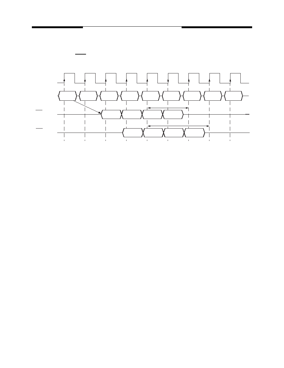
1. Bank Activate Command Cycle
(CAS latency = 3)
2. Burst Read Operation
(Burst Length = 4, CAS latency = 2, 3)
ADDRESS
CLK
T0
T
T1
T
T
T
T
COMMAND
NOP
NOP
NOP
Bank A
Row Addr.
Bank A
Activate
Write A
with Auto
Bank A
Col. Addr.
. . . . . . . . . .
. . . . . . . . . .
. . . . . . . . . .
Bank B
Activate
Bank A
Row Addr.
Bank A
Activate
t
RCD
: "H" or "L"
t
RC
Precharge
t
RRD
Bank B
Row Addr.
COMMAND
READ A
NOP
NOP
NOP
NOP
NOP
NOP
NOP
DOUT A
0
CAS latency = 2
t
CK3,
I/O's
CAS latency = 3
DOUT A
1
DOUT A
2
DOUT A
3
NOP
CLK
T0
T2
T1
T3
T4
T5
T6
T7
T8
t
CK2,
I/O's
DOUT A
0
DOUT A
1
DOUT A
2
DOUT A
3

19
V55C2256164VB Rev. 1.0 April 2005
ProMOS TECHNOLOGIES
V55C2256164VB
3. Read Interrupted by a Read
(Burst Length = 4, CAS latency = 2, 3)
4.1 Read to Write Interval
(Burst Length = 4, CAS latency = 3)
COMMAND
READ A
READ B
NOP
NOP
NOP
NOP
NOP
NOP
t
CK2,
I/O's
CAS latency = 2
t
CK3,
I/O's
CAS latency = 3
NOP
CLK
T0
T2
T1
T3
T4
T5
T6
T7
T8
DOUT B
0
DOUT B
1
DOUT B
2
DOUT B
3
DOUT A
0
DOUT B
0
DOUT B
1
DOUT B
2
DOUT B
3
DOUT A
0
COMMAND
NOP
READ A
NOP
NOP
NOP
NOP
WRITE B
NOP
NOP
DQM
DOUT A0
DIN B0
DIN B1
DIN B2
Must be Hi-Z before
the Write Command
I/O's
Minimum delay between the Read and Write Commands = 4+1 = 5 cycles
CLK
T0
T2
T1
T3
T4
T5
T6
T7
T8
t
DQZ
t
DQW
: "H" or "L"

20
V55C2256164VB Rev. 1.0 April 2005
ProMOS TECHNOLOGIES
V55C2256164VB
4.2 Minimum Read to Write Interval
(Burst Length = 4, CAS latency = 2)
4.3 Non-Minimum Read to Write Interval
(Burst Length = 4, CAS latency = 2, 3)
COMMAND
NOP
BANK A
NOP
READ A
WRITE A
NOP
NOP
NOP
DQM
DIN A0
DIN A1
DIN A2
DIN A3
Must be Hi-Z before
the Write Command
t
CK2,
I/O's
CAS latency = 2
CLK
T0
T2
T1
T3
T4
T5
T6
T7
T8
NOP
ACTIVATE
1 Clk Interval
t
DQZ
t
DQW
: "H" or "L"
NOP
READ A
NOP
NOP
READ A
NOP
WRITE B
NOP
NOP
DQM
DIN B0
DIN B1
DIN B2
t
CK1,
I/O's
CAS latency = 2
t
CK2,
I/O's
CAS latency = 3
CLK
T0
T2
T1
T3
T4
T5
T6
T7
T8
DOUT A0
COMMAND
DIN B0
DIN B1
DIN B2
DOUT A1
DOUT A0
Must be Hi-Z before
the Write Command
t
DQZ
t
DQW
: "H" or "L"

21
V55C2256164VB Rev. 1.0 April 2005
ProMOS TECHNOLOGIES
V55C2256164VB
5. Burst Write Operation
(Burst Length = 4, CAS latency = 2, 3)
6.1 Write Interrupted by a Write
(Burst Length = 4, CAS latency = 2, 3)
COMMAND
NOP
WRITE A
NOP
NOP
NOP
NOP
NOP
NOP
I/O's
DIN A0
DIN A1
DIN A2
DIN A3
NOP
CLK
T0
T2
T1
T3
T4
T5
T6
T7
T8
Extra data is ignored after
The first data element and the Write
are registered on the same clock edge.
termination of a Burst.
don't care
COMMAND
NOP
WRITE A
WRITE B
NOP
NOP
NOP
NOP
NOP
I/O's
DIN A
0
DIN B
0
DIN B
1
DIN B
2
NOP
DIN B
3
CLK
T0
T2
T1
T3
T4
T5
T6
T7
T8
1 Clk Interval
22
V55C2256164VB Rev. 1.0 April 2005
ProMOS TECHNOLOGIES
V55C2256164VB
6.2 Write Interrupted by a Read
(Burst Length = 4, CAS latency = 2, 3)
7. Burst Write with Auto-Precharge
Burst Length = 2, CAS latency = 2, 3)
COMMAND
NOP
WRITE A
READ B
NOP
NOP
NOP
NOP
NOP
NOP
t
CK2,
I/O's
CAS latency = 2
DIN A0
t
CK3,
I/O's
CAS latency = 3
DIN A0
CLK
T0
T2
T1
T3
T4
T5
T6
T7
T8
DOUT B3
DOUT B0
DOUT B1
DOUT B2
DOUT B3
don't care
don't care
don't care
DOUT B0
DOUT B1
DOUT B2
Input data must be removed from the I/O's at least one clock
cycle before the Read dataAPpears on the outputs to avoid
data contention.
COMMAND
NOP
NOP
NOP
WRITE A
Auto-Precharge
CLK
T0
T2
T1
T3
T4
T5
T6
T7
T8
NOP
BANK A
ACTIVE
NOP
NOP
DIN A0
DIN A1
I/O's
CAS latency = 3
I/O's
CAS latency = 2
Begin Autoprecharge
Bank can be reactivated after trp
*
t
WR
t
RP
DIN A0
DIN A1
t
WR
t
RP
NOP
*
23
V55C2256164VB Rev. 1.0 April 2005
ProMOS TECHNOLOGIES
V55C2256164VB
7.2 Burst Read with Auto-Precharge
Burst Length = 4, CAS latency = 2, 3)
COMMAND
READ A
NOP
NOP
NOP
NOP
NOP
NOP
t
CK2,
I/O's
CAS latency = 2
t
CK3,
I/O's
CAS latency = 3
CLK
T0
T2
T1
T3
T4
T5
T6
T7
T8
DOUT A3
DOUT A
tRP
tRP
*
*
*
0
DOUT A1
DOUT A2
DOUT A3
DOUT A
Begin Autoprecharge
Bank can be reactivated after tRP
0
DOUT A1
DOUT A2
NOP
NOP

24
V55C2256164VB Rev. 1.0 April 2005
ProMOS TECHNOLOGIES
V55C2256164VB
8.1 Termination of a Burst Read Operation
(CAS latency = 2, 3)
8.2 Termination of a Burst Write Operation
(CAS latency = 2, 3)
COMMAND
READ A
NOP
NOP
NOP
Burst
NOP
NOP
NOP
NOP
t
CK2,
I/O's
CAS latency = 2
t
CK3,
I/O's
CAS latency = 3
Stop
CLK
T0
T2
T1
T3
T4
T5
T6
T7
T8
DOUT A
0
DOUT A
1
DOUT A
2
DOUT A
3
DOUT A
0
DOUT A
1
DOUT A
2
DOUT A
3
COMMAND
NOP
WRITE A
NOP
NOP
Burst
NOP
NOP
NOP
NOP
DIN A0
DIN A1
DIN A2
Stop
CLK
T0
T2
T1
T3
T4
T5
T6
T7
T8
Input data for the Write is masked.
I/O's
CAS latency = 2,3
don't care

25
V55C2256164VB Rev. 1.0 April 2005
ProMOS TECHNOLOGIES
V55C2256164VB
CLK
CKE
CS
I/
O
RAS
CAS
WE
B
A
DQM
9
.
1
A
C
P
a
ra
m
e
t
e
rs
f
o
r
W
r
it
e
Ti
m
i
n
g
T2
T
3
T4
T0
T1
T6
T7
T8
T9
T5
T1
1
T1
2
T1
3
T
1
4
T1
0
T1
6
T1
7
T1
8
T
1
9
T1
5
T
2
2
T2
0
T2
1
Hi
-
Z
AP
Bur
s
t
L
engt
h
= 4,
CAS
La
t
enc
y
=
2
A
d
d
r
t
CK
S
t
CS
t
CH
t
CK
H
t
AS
t
RC
D
t
RC
t
RP
t
DS
A
c
ti
v
a
te
C
o
mma
nd
Ba
n
k
A
Wr
it
e
w
i
t
h
A
u
to P
r
ec
har
ge
C
o
m
m
and
B
ank
A
A
c
ti
v
a
te
C
o
mman
d
B
ank
B
Wr
it
e
w
i
t
h
A
u
to
P
r
ec
har
ge
C
o
mm
and
B
ank
B
A
c
ti
v
a
te
C
o
m
m
and
B
ank
A
Wr
it
e
C
o
mma
nd
Ba
n
k
A
Pr
e
c
h
a
r
g
e
C
o
m
m
and
B
ank
A
Ac
t
i
v
a
t
e
C
o
mm
and
Ba
n
k
A
t
DH
Ax
0
Ax
3
Ax
2
Ax
1
Bx
0
Bx
3
Bx
2
Bx
1
Ay
0
Ay
3
Ay
2
Ay
1
t
CK
2
t
CH
t
CL
B
egi
n A
u
to P
r
ec
har
ge
B
ank
A
Be
g
i
n
Au
t
o
Pr
e
c
h
a
r
g
e
Ba
n
k
B
t
DP
L
t
RR
D
A
c
ti
v
a
te
C
o
m
m
and
B
ank
B
RA
y
CB
x
R
A
y
RA
y
RB
x
RB
x
CAx
RB
y
RB
y
RA
z
RA
z
RA
x
RA
x
t
AH
26
V55C2256164VB Rev. 1.0 April 2005
ProMOS TECHNOLOGIES
V55C2256164VB
\
CLK
CKE
CS
I/O
RAS
CAS
WE
B
A
DQM
9
.
2
AC P
a
ra
m
e
t
e
rs
f
o
r
Re
a
d
T
i
m
i
ng
T2
T3
T
4
T0
T1
T6
T7
T8
T9
T5
T1
1
T1
2
T1
3
T1
0
Hi
-
Z
AP
Bur
s
t
Leng
t
h
= 2,
CAS
Lat
e
n
cy = 2
A
d
d
r
t
CS
t
CH
t
CK
H
t
AS
t
AH
t
RRD
t
RC
D
t
RA
S
t
LZ
A
c
ti
v
a
te
C
o
mmand
B
ank
A
A
c
ti
v
a
te
C
o
mmand
B
ank
B
A
c
ti
v
a
te
C
o
m
m
and
B
ank
A
P
r
ec
har
ge
C
o
mm
and
B
ank
A
t
CK
S
t
CK
2
Ax
0
Ax
1
R
ead
C
o
mman
d
Ba
n
k
A
R
ead w
i
th
Au
t
o
Pr
e
c
h
a
r
g
e
C
o
mmand
B
ank
B
t
RC
t
RP
t
AC
2
t
AC
2
t
OH
t
HZ
t
CH
t
CL
Bx
0
B
egi
n A
u
to
Pr
e
c
h
a
r
g
e
B
ank
B
Bx
1
t
HZ
RB
x
R
A
y
RB
x
RB
x
RA
y
CA
x
RA
x
RA
x

27
V55C2256164VB Rev. 1.0 April 2005
ProMOS TECHNOLOGIES
V55C2256164VB
\
1
0
.
Mode
R
e
gis
t
e
r
S
e
t
CLK
CKE
CS
RAS
CAS
WE
BA
T2
T3
T4
T0
T1
T6
T7
T8
T9
T5
T11
T12
T13
T14
T10
T16
T17
T18
T19
T15
T22
T20
T21
AP
Addr
Precharge
Command
All Banks
Mode Register
Set Command
Any
Command
Address Key
2 Clock min.

28
V55C2256164VB Rev. 1.0 April 2005
ProMOS TECHNOLOGIES
V55C2256164VB
\
1
1
.
P
o
w
e
r
on S
e
que
nc
e
a
n
d
Aut
o Re
f
r
e
s
h
(
CBR)
CLK
CKE
CS
I/O
RAS
CAS
WE
BA
DQM
TT
T
T0
TT
T
TT
T
T
T
TT
T1
T
T
TT
TT
T
T
Hi-Z
AP
Addr
Precharge
Command
All Banks
t
RP
Minimum of 2 Refresh Cycles are required
1st Auto Refresh
Command
t
RC
High level
is required
2nd Auto Refresh
Command
Inputs must be
stable for 200
s
Low Power Mode Register
Set Command
2 Clock min.
Mode Register
Address Key
Set Command

29
V55C2256164VB Rev. 1.0 April 2005
ProMOS TECHNOLOGIES
V55C2256164VB
\
1
2
. P
o
w
e
r Dow
n
Mode
Bur
s
t
L
engt
h
= 4,
CAS
La
t
enc
y
=
2
CLK
CKE
CS
I/O
RAS
CAS
WE
BA
DQM
T2
T3
T4
T0
T1
T6
T7
T8
T9
T5
T11
T12
T13
T14
T10
T16
T17
T18
T19
T15
T22
T20
T21
Hi-Z
AP
Addr
t
CKSP
RAx
RAx
Activate
Command
Bank A
Precharge
Command
Bank A
Power Down
Mode Entry
Power Down
Mode Exit
Any
Command

30
V55C2256164VB Rev. 1.0 April 2005
ProMOS TECHNOLOGIES
V55C2256164VB
1
3
. S
e
lf
Re
f
r
e
s
h (
E
nt
ry
a
nd E
x
it
)
BA
Addr
AP
t
CLK
CKE
CS
I/O
RAS
CAS
WE
D
QM
T2
T3
T4
T0
T1
T
T
TT
T5
T
T
TT
T
T
T
TT
TT
T
T
Hi-Z
All Banks
must be idle
Self Refresh
Entry
Begin Self Refresh
Exit Command
t
SREX
Self Refresh Exit
Command issued
Self Refresh
Exit
t
RC
CKSR
31
V55C2256164VB Rev. 1.0 April 2005
ProMOS TECHNOLOGIES
V55C2256164VB
\
1
4
. Aut
o
Re
f
r
e
s
h (
CBR)
Bu
r
s
t
L
engt
h
= 4,
CAS
L
a
te
n
c
y
=
2
CLK
CKE
CS
I/O
RAS
CAS
WE
BA
DQM
T2
T3
T4
T0
T1
T6
T7
T8
T9
T5
T11
T12
T13
T14
T10
T16
T17
T18
T19
T15
T22
T20
T21
Hi-Z
AP
Addr
Ax0
Ax1
Activate
Command
Read
Command
Precharge
Command
Auto Refresh
Command
Auto Refresh
Command
t
RC
t
RP
t
RC
t
CK2
All Banks
CAx
RAx
RAx
Bank A
Bank A
Ax2
Ax3
(Minimum Interval)

32
V55C2256164VB Rev. 1.0 April 2005
ProMOS TECHNOLOGIES
V55C2256164VB
\
)
1
5
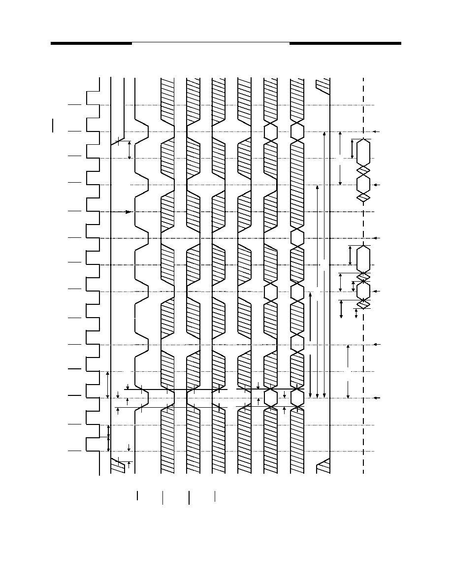
.1
Ra
n
dom
Colum
n
Re
a
d
(
P
a
g
e
w
i
t
h
i
n
s
a
m
e
Ba
nk
)
(
1
of
2
)
Bur
s
t
Len
gt
h
=
4,
CAS
Lat
ency
= 2
CLK
CKE
CS
I/O
RAS
CAS
WE
BA
DQM
T2
T3
T4
T0
T1
T6
T7
T8
T9
T5
T11
T12
T13
T14
T10
T16
T17
T18
T19
T15
T22
T20
T21
Hi-Z
AP
Addr
Activate
Command
Bank A
CAx
Read
Command
Bank A
CAy
Read
Command
Bank A
Aw0
Aw1
Aw2
Aw3
Ax0
Ax1
Ay0
Ay1
Az0
Az1
Az2
Az3
Ay2
Ay3
CAw
Read
Command
Bank A
RAw
RAw
Precharge
Command
Bank A
Activate
Command
Bank A
CAz
Read
Command
Bank A
RAz
RAz
t
CK2

33
V55C2256164VB Rev. 1.0 April 2005
ProMOS TECHNOLOGIES
V55C2256164VB
\
)
1
5
.2
Ra
ndom
Colum
n
Re
a
d
(
P
a
g
e
w
i
t
h
i
n
s
a
m
e
Ba
nk
)
(
2
of
2
)
Bur
s
t
L
engt
h
= 4,
CAS
La
t
enc
y
=
3
CLK
CKE
CS
I/O
RAS
CAS
WE
BA
D
QM
T2
T3
T4
T0
T1
T6
T7
T8
T9
T5
T11
T12
T13
T14
T10
T16
T17
T18
T19
T15
T22
T20
T21
Hi-Z
AP
Addr
Activate
Command
Bank A
CAx
Read
Command
Bank A
CAy
Read
Command
Bank A
Aw0
Aw1
Aw2
Aw3
Ax0
Ax1
Ay0
Ay1
Ay2
Ay3
CAw
Read
Command
Bank A
RAw
RAw
Precharge
Command
Bank A
Activate
Command
Bank A
CAz
Read
Command
Bank A
RAz
RAz
t
CK3

34
V55C2256164VB Rev. 1.0 April 2005
ProMOS TECHNOLOGIES
V55C2256164VB
\
)
1
6
.1
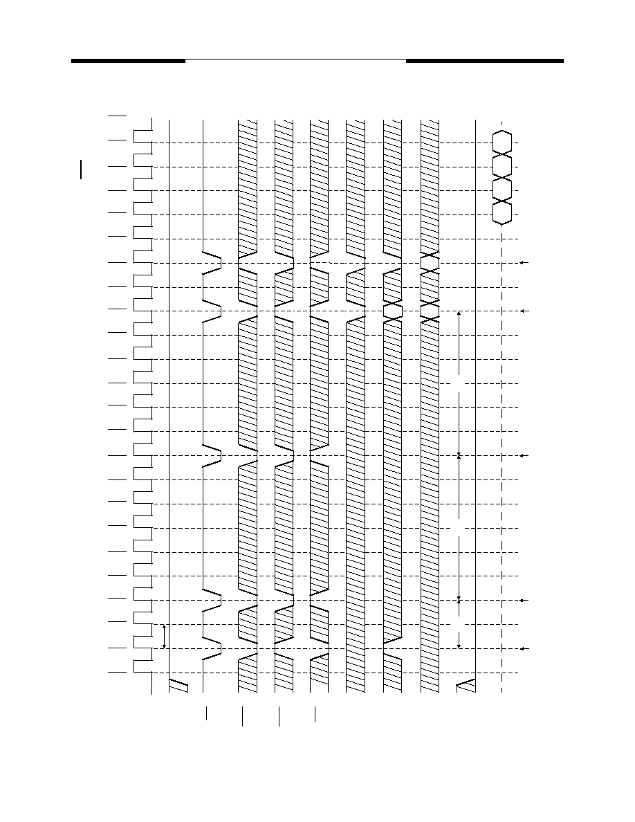
Ra
ndom
Colum
n
Wr
it
e
(
P
a
g
e
w
i
t
h
in s
a
m
e
Ba
nk
)
(
1
of
2
)
Bur
s
t
L
engt
h
= 4,
CAS
La
t
enc
y
=
2
CLK
CKE
CS
I/O
RAS
CAS
WE
BA
DQM
T2
T3
T4
T0
T1
T6
T7
T8
T9
T5
T11
T12
T13
T14
T10
T16
T17
T18
T19
T15
T22
T20
T21
Hi-Z
AP
Addr
CBx
Write
Command
Bank B
CBy
Write
Command
Bank B
Precharge
Command
Bank B
DBw0
DBw3
DBw2
DBw1
DBx1
DBx0
DBy0
DBy3
DBy2
DBy1
DBz0
DBz3
DBz2
DBz1
t
CK2
Activate
Command
Bank B
CAx
Write
Command
Bank B
RAw
RAw
Activate
Command
Bank B
CBz
Write
Command
Bank B
RBz
RBz
Activate
Command
Bank B
CBz
Write
Command
Bank B
RBz
RBz

35
V55C2256164VB Rev. 1.0 April 2005
ProMOS TECHNOLOGIES
V55C2256164VB
\
)
1
6
.2
Ra
ndom
Colum
n
Wr
it
e
(
P
a
g
e
w
i
t
h
in s
a
m
e
Ba
nk
)
(
2
of
2
)
Bur
s
t
L
engt
h
= 4,
CAS
La
t
enc
y
=
3
CLK
CKE
CS
I/O
RAS
CAS
WE
BA
DQM
T2
T3
T4
T0
T1
T6
T7
T8
T9
T5
T11
T12
T13
T14
T10
T16
T17
T18
T19
T15
T22
T20
T21
Hi-Z
AP
Addr
CBx
Write
Command
Bank B
CBy
Write
Command
Bank B
Precharge
Command
Bank B
DBw0
DBw3
DBw2
DBw1
DBx1
DBx0
DBy0
DBy3
DBy2
DBy1
DBz0
DBz1
t
CK3
Activate
Command
Bank B
CBz
Write
Command
Bank B
RBz
RBz
Activate
Command
Bank B
CBz
Write
Command
Bank B
RBz
RBz

36
V55C2256164VB Rev. 1.0 April 2005
ProMOS TECHNOLOGIES
V55C2256164VB
1
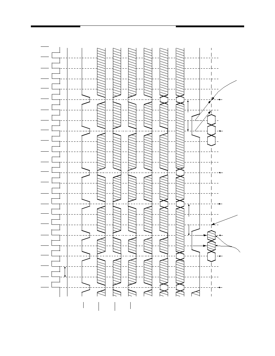
7
.
1
Ra
ndom
Row
Re
a
d
(
I
nt
e
r
l
e
a
v
i
ng Ba
nk
s
)
(
1
of
2
)
Bur
s
t
Le
ngt
h =
8,
CAS
Lat
enc
y =
2
CLK
CKE
CS
I/O
RAS
CAS
WE
A11(BS)
DQM
T2
T3
T4
T0
T1
T6
T7
T8
T9
T5
T11
T12
T13
T14
T10
T16
T17
T18
T19
T15
T22
T20
T21
Hi-Z
A10
A0 - A9
CBy
Read
Command
Bank B
Read
Command
Bank A
Bx0
Bx1
Bx2
Bx3
Bx4
Bx5
Bx6
Bx7
By0
By1
t
CK2
High
t
RCD
t
AC2
t
RP
CAx
Precharge
Command
Bank B
Ax0
Ax1
Ax2
Ax3
Ax4
Ax5
Ax6
Ax7
Activate
Command
Bank B
RBx
RBx
Activate
Command
Bank A
RAx
RAx
CBx
Read
Command
Bank B
Activate
Command
Bank B
RBy
RBy

37
V55C2256164VB Rev. 1.0 April 2005
ProMOS TECHNOLOGIES
V55C2256164VB
17.
2 R
a
n
d
o
m
R
o
w
R
e
ad
(I
n
t
e
r
l
e
avi
n
g
B
a
n
k
s) (2
o
f
2)
Bur
s
t
Le
ngt
h =
8,
CAS
Lat
enc
y =
3
CLK
CKE
CS
I/O
RAS
CAS
WE
A
11(BS)
DQM
T2
T3
T4
T0
T1
T6
T7
T8
T9
T5
T11
T12
T13
T14
T10
T16
T17
T18
T19
T15
T22
T20
T21
Hi-Z
A10
A0 - A9
CBy
Read
Command
Bank B
By0
t
CK3
High
t
AC3
Activate
Command
Bank B
RBx
RBx
Activate
Command
Bank A
RAx
RAx
CBx
Read
Command
Bank B
Activate
Command
Bank B
RBy
RBy
t
RCD
Precharge
Command
Bank B
CAx
Read
Command
Bank A
t
RP
Bx0
Bx1
Bx2
Bx3
Bx4
Bx5
Bx6
Bx7
Ax0
Ax1
Ax2
Ax3
Ax4
Ax5
Ax6
Ax7
Precharge
Command
Bank A

38
V55C2256164VB Rev. 1.0 April 2005
ProMOS TECHNOLOGIES
V55C2256164VB
1
8
.1
Ra
ndom
Row
Wri
t
e
(
I
nt
e
r
le
a
v
ing Ba
nk
s
)
(
1
of
2
)
Bu
r
s
t
Lengt
h =
8,
CAS
L
a
te
n
c
y
=
2
CLK
CKE
CS
I/O
RAS
CAS
WE
A
11(BS)
DQM
T2
T3
T4
T0
T1
T6
T7
T8
T9
T5
T11
T12
T13
T14
T10
T16
T17
T18
T19
T15
T22
T20
T21
Hi-Z
A10
A0 - A9
t
CK2
High
t
RCD
t
RP
Write
Command
Bank A
CAy
DAx0
DAx3
DAx2
DAx1
DAx4
DAx7
DAx6
DAx5
DBx0
DBx3
DBx2
DBx1
DBx4
DBx7
DBx6
DBx5
DAy0
DAy3
DAy2
DAy1
t
DPL
Write
Command
Bank A
CAX
Activate
Command
Bank A
RAx
RAx
Activate
Command
Bank B
RBx
RBx
CBx
Precharge
Command
Bank A
Write
Command
Bank B
Activate
Command
Bank A
RAy
RAy
CAy
Precharge
Command
Bank B
Write
Command
Bank A
DAy4
t
DPL

39
V55C2256164VB Rev. 1.0 April 2005
ProMOS TECHNOLOGIES
V55C2256164VB
1
8
.2
Ra
ndom
Row
Wri
t
e
(
I
nt
e
r
le
a
v
ing Ba
nk
s
)
(
2
of
2
)
Bu
r
s
t
Lengt
h =
8,
CAS
L
a
te
n
c
y
=
3
CLK
CKE
CS
I/O
RAS
CAS
WE
A11(BS)
DQM
T2
T3
T4
T0
T1
T6
T7
T8
T9
T5
T11
T12
T13
T14
T10
T16
T17
T18
T19
T15
T22
T20
T21
Hi-Z
A10
A0 - A9
t
CK3
High
DAx0
DAx3
DAx2
DAx1
DAx4
DAx7
DAx6
DAx5
DBx0
DBx3
DBx2
DBx1
DBx4
DBx7
DBx6
DBx5
DAy2
DAy1
DAy0
Write
Command
Bank A
CAX
Activate
Command
Bank B
RBx
RBx
Activate
Command
Bank A
RAy
RAy
DAy3
t
DPL
CBx
Write
Command
Bank B
Precharge
Command
Bank A
Write
Command
Bank A
CAy
Precharge
Command
Bank B
t
RP
t
DPL
t
RCD
Activate
Command
Bank A
RAx
RAx

40
V55C2256164VB Rev. 1.0 April 2005
ProMOS TECHNOLOGIES
V55C2256164VB
1
9
.1
P
r
e
c
h
a
r
ge
T
e
r
m
ina
t
ion of
a
Burs
t
(
1
of
2
)
Bur
s
t
L
engt
h =
8,
C
A
S Lat
enc
y
= 2
CLK
CKE
CS
I/O
RAS
CAS
WE
BA
DQM
T2
T3
T4
T0
T1
T6
T7
T8
T9
T5
T11
T12
T13
T14
T10
T16
T17
T18
T19
T15
T22
T20
T21
Hi-Z
AP
Addr
t
CK2
Precharge
Command
Bank A
DAx0
DAx3
DAx2
DAx1
Precharge Termination
of a Write Burst. Write
data is masked.
Ay0
Ay1
Ay2
Precharge Termination
of a Read Burst.
Precharge
Command
Bank A
t
RP
Activate
Command
Bank A
RAx
RAx
Write
Command
Bank A
CAx
CAy
Read
Command
Bank A
High
Activate
Command
Bank A
RAy
RAy
t
RP
Activate
Command
Bank A
RAz
RAz
CAz
Read
Command
Bank A
Az0
Az1
Az2
Precharge
Command
Bank A
t
RP
41
V55C2256164VB Rev. 1.0 April 2005
ProMOS TECHNOLOGIES
V55C2256164VB
1
9
.2
P
r
e
c
h
a
r
ge
T
e
r
m
ina
t
ion of
a
Burs
t
(
2
of
2
)
Bur
s
t
Leng
t
h
= 4,
8,
CAS Lat
ency
= 3
CLK
CKE
CS
I/O
RAS
CAS
WE
BA
D
QM
T2
T3
T4
T0
T1
T6
T7
T8
T9
T5
T11
T12
T13
T14
T10
T16
T17
T18
T19
T15
T22
T20
T21
Hi-Z
AP
Addr
t
CK3
Precharge
Command
Bank A
DAx0
Precharge Termination
of a Write Burst.
Write Data
is masked
Ay0
Ay1
Ay2
Precharge Termination
Precharge
Command
Bank A
t
RP
Activate
Command
Bank A
RAx
RAx
Write
Command
Bank A
CAx
CAy
Read
Command
Bank A
High
Activate
Command
Bank A
RAy
RAy
t
RP
Activate
Command
Bank A
RAz
RAz
of a Read Burst.

42
V55C2256164VB Rev. 1.0 April 2005
ProMOS TECHNOLOGIES
V55C2256164VB
20.1 Deep Power Down Mode Entry
The deep power down mode has to be maintained for a minimum of 100µs.
CLK
CKE
CS
WE
CAS
RAS
Addr.
DQM
DQ
input
DQ
output
High-Z
t
RP
Precharge Command
Deep Power Down Entry
Deep Power Down Mode
DP1.vsd
Normal Mode

43
V55C2256164VB Rev. 1.0 April 2005
ProMOS TECHNOLOGIES
V55C2256164VB
20.2 Deep Power Down Exit
The deep power down mode is exited by asserting CKE high. After the exit, the following sequence is needed to
enter a new command:
1. Maintain NOP input conditions for a minimum of 200
µs
2. Issue precharge commands for all banks of the device
3. Issue eight or more autorefresh commands
4. Issue a mode register set command to initialize the mode register
5. Issue an extended mode register set command to initialize the extende mode register
CLK
CK E
CS
RAS
CAS
WE
tRP
All banks
200
s
Au to
Deep Power Do wn
Auto
tRC
Mode
exi t
prec harge
refresh
refresh
Register
Set
Exte nded
Mode
Regis ter
Set
New
Com mand
Acce pted
Here

44
V55C2256164VB Rev. 1.0 April 2005
ProMOS TECHNOLOGIES
V55C2256164VB
Package Diagram
54-Pin Plastic TSOP-II (400 mil)
0.881 -0.01
[22.38 -0.25]
0.031
[0.80]
.004 [0.1]
54
Index Marking
M
28
1
Does not include plastic or metal protrusion of 0.15 max. per side
1
27
0.047 [1.20] MAX
0.04
±0.002
[1
±0.05]
Unit in inches [mm]
0.400
±0.005
[10.16
±0.13]
0.463
± 0.008
[11.76
± 0.20]
0.006 [0.15] MAX
+0.004
-0.002
0
∞
≠5
∞
0.024
± 0.008
[0.60
± .020]
1
0.006
+0.01
-0.05
0.15
.008 [0.2]
54x
+0.002
-0.004
0.016
+0.05
-0.10
0.40

45
V55C2256164VB Rev. 1.0 April 2005
ProMOS TECHNOLOGIES
V55C2256164VB
FBGA-BOC package 54 BGA package with 3 depop. rows
FBGA-BOC package 54 BGA package with 3 depop. rows
Units (mm)
13

46
V55C2256164VB Rev. 1.0 April 2005
ProMOS TECHNOLOGIES
V55C2256164VB
WORLDWIDE OFFICES
© Copyright ,ProMOS TECHNOLOGY.
Printed in U.S.A.
The information in this document is subject to change without
notice.
ProMOS TECH makes no commitment to update or keep cur-
rent the information contained in this document. No part of this
document may be copied or reproduced in any form or by any
means without the prior written consent of ProMOS TECH.
ProMOS TECH subjects its products to normal quality control
sampling techniques which are intended to provide an assurance
of high quality products suitable for usual commercial applica-
tions. ProMOS TECH does not do testing appropriate to provide
100% product quality assurance and does not assume any liabil-
ity for consequential or incidental arising from any use of its prod-
ucts. If such products are to be used in applications in which
personal injury might occur from failure, purchaser must do its
own quality assurance testing appropriate to such applications.
TAIWAN(Taipei)
7F, NO. 102 MIN-CHUAN E. ROAD
SEC. 3, Taipei, Taiwan, R.O.C
PHONE: 886-2-2545-1213
FAX: 886-2-2545-1209
NO. 19 LI HSIN ROAD
SCIENCE BASED IND. PARK
HSIN CHU, TAIWAN, R.O.C.
PHONE: 886-3-566-3952
FAX: 886-3-578-6028
JAPAN
ONZE 1852 BUILDING 6F
2-14-6 SHINTOMI, CHUO-KU
TOKYO 104-0041
PHONE: 81-3-3537-1400
FAX: 81-3-3537-1402
USA(West)
3910 NORTH FIRST STREET
SAN JOSE, CA 95134
PHONE: 408-433-6000
FAX: 408-433-0952
SALES OFFICES:
TAIWAN(Hsinchu)
USA(East)
25 Creekside Road
Hopewell Jct, NY 12533
PHONE:845-223-1689
FAX:845-223-1684