MDC5001T≠1/10
1
3
2
MDC5001T1
SOT-363
CASE 419B≠01 STYLE 19
6
4
5
Low Voltage Bias Stabilizer with Enable
SILICON
SMALLBLOCK
TM
INTEGRATED CIRCUIT
∑ Maintains Stable Bias Current in N≠Type Discrete Bipolar Junction and
Field Effect Transistors
∑ Provides Stable Bias Using a Single Component Without Use of Emitter
Ballast and Bypass Components
∑ Operates Over a Wide Range of Supply Voltages Down to 1.8 Vdc
∑ Reduces Bias Current Variation Due to Temperature and Unit≠to≠Unit
Parametric Changes
∑ Consumes <0.5 mW at V
CC
= 2.75 V
∑ Active High Enable is CMOS Compatible
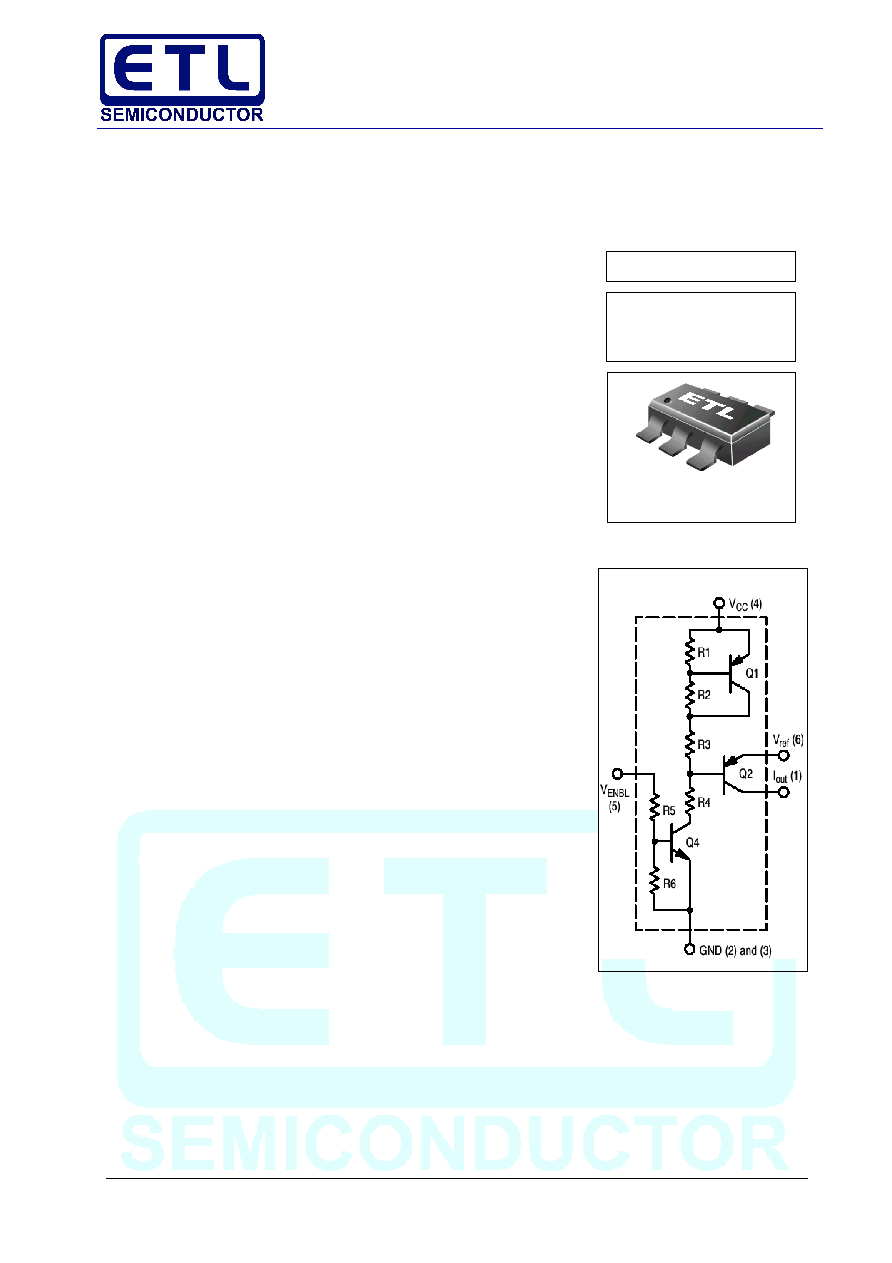
This device provides a reference voltage and acts as a DC feedback ele-
ment around an external discrete, NPN BJT or N≠Channel FET. It allows the
external transistor to have its emitter/source directly grounded and still oper-
ate with a stable collector/drain DC current. It is primarily intended to stabilize
the bias of discrete RF stages operating from a low voltage regulated supply,
but can also be used to stabilize the bias current of any linear stage in order to
eliminate emitter/source bypassing and achieve tighter bias regulation over
temperature and unit variations. The "ENABLE" polarity nulls internal current,
Enable current, and RF transistor current in "STANDBY." This device is in-
tended to replace a circuit of three to six discrete components.
The combination of low supply voltage, low quiescent current drain, and
small package make the MDC5001T1 ideal for portable communications ap-
plications such as:
∑ Cellular Telephones
∑ Pagers
∑ PCN/PCS Portables
∑ GPS Receivers
∑ PCMCIA RF Modems
∑ Cordless Phones
∑ Broadband and Multiband Transceivers and Other Portable Wireless
Products.
INTERNAL CIRCUIT DIAGRAM

MDC5001T≠2/10
MAXIMUM RATINGS
Rating
Symbol
Value
Unit
Power Supply Voltage
V
CC
15
V
dc
Ambient Operating Temperature Range
T
A
≠40 to +85
∞C
Storage Temperature Range
T
stg
≠65 to +150
∞C
Junction Temperature
T
J
150
∞C
Collector Emitter Voltage (Q2)
V
CEO
≠15
V
Enable Voltage (Pin 5)
V
ENBL
V
CC
V
THERMAL CHARACTERISTICS
Characteristic
Symbol
Max
Unit
Total Device Power Dissipation
P D
mW
(FR≠5 PCB of 1, ◊ 0.75, ◊ 0.062,, T
A
= 25∞C)
150
Derate above 25∞C
1.2
mW/∞C
Thermal Resistance, Junction to Ambient
R
JA
833
∞C/W
ELECTRICAL CHARACTERISTICS (T
A
= 25∞C unless otherwise noted)
Characteristic
Symbol
Min
Typ
Max
Unit
Recommended Operating Supply Voltage
V
CC
1.8
2.75
10
Volts
Power Supply Current (V
CC
= 2.75 V)
I
CC
--
130
200
mA
V
ref
, I
out
are unterminated
See Figure 8
Q2 Collector Emitter Breakdown Voltage
V
(BR)CEO2
15
Volts
(I
C2
= 10
µ
A, I
B2
= 0)
Reference Voltage (V
ENBL
= V
CC
= 2.75 V, V
out
= 0.7 V)
V ref
Volts
(I
out
= 30
µ
A)
2.050
2.075
2.100
(I
out
= 150
µ
A)
2.110
2.135
2.160
See Figure 1
Reference Voltage (V
ENBL
= V
CC
= 2.75 V, V
out
= 0.7 V,
≠40∞C < T
A
<+85∞C)
V
CC
Pulse Width = 10 mS, Duty Cycle = 1%
V
ref
mV
(I
out
= 10
µ
A)
±5.0
±10
(I
out
= 30
µ
A)
±15
±30
(I
out
= 100
µ
A)
±25
±50
See Figures 2 and 11
MDC5001T1

MDC5001T≠3/10
MDC5001T1
The following SPICE models are provided as a convenience to the user and every effort has been ade
to insure their accuracy. However, no responsibility for their accuracy is assumed by ON Semiconductor.
.MODEL Q4 NPN
BF = 136
BR = 0.2
CJC = 318.6 f
CJE = 569.2 f
CJS = 1.9 p
EG = 1.215
FC = 0.5
IKF = 24.41 m
IKR = 0.25
IRB = 0.0004
IS = 256E≠18
ISC = 1 f
ISE = 500E≠18
ITF = 0.9018
MJC = 0.2161
MJE = 0.3373
MJS = 0.13
NC = 1.09
NE = 1.6
NF = 1.005
RB = 140
RBM = 70
RC = 180
RE = 1.6
TF = 553.6 p
TR = 10 n
VAF = 267.6
VAR = 12
VJC = 0.4172
VJE = 0.7245
VJS = 0.39
VTF = 10
XTB = 1.5
XTF = 2.077
XTI = 3
.MODEL Q1, Q2 PNP
BF = 87
BR = 0.6
CJC = 800E≠15
CJE = 46E≠15
EG = 1.215
FC = 0.5
IKF = 3.8E≠04
IKR = 2.0
IRB = 0.9E≠3
IS = 1.027E≠15
ISC = 10E≠18
ISE = 1.8E≠15
ITF = 2E≠3
MJC = 0.2161
MJE = 0.2161
NC = 0.8
NE = 1.38
NF = 1.015
NK = 0.5
NR = 1.0
RB = 720
RBM = 470
RC = 180
RE = 26
TF = 15E≠9
TR = 50E≠09
VAF = 54.93
VAR = 20
VAR = 20
VJC = 0.4172
VJE = 0.4172
VTF = 10
XTB = 1.5
XTF = 2.0
XTI = 3
These models can be retrieved
electronically by accessing the ON
Semiconductor Web page at
http://design≠net.sps.mot.com/models
and searching the section on
SMALLBLOCKE models
RESISTOR VALUES
R
1
= 12 K
R
2
= 6 K
R
3
= 3.4 K
R
4
= 12 K
R
5
= 20 K
R
6
= 40 K
MDC5001T≠5/10
MDC5001T1
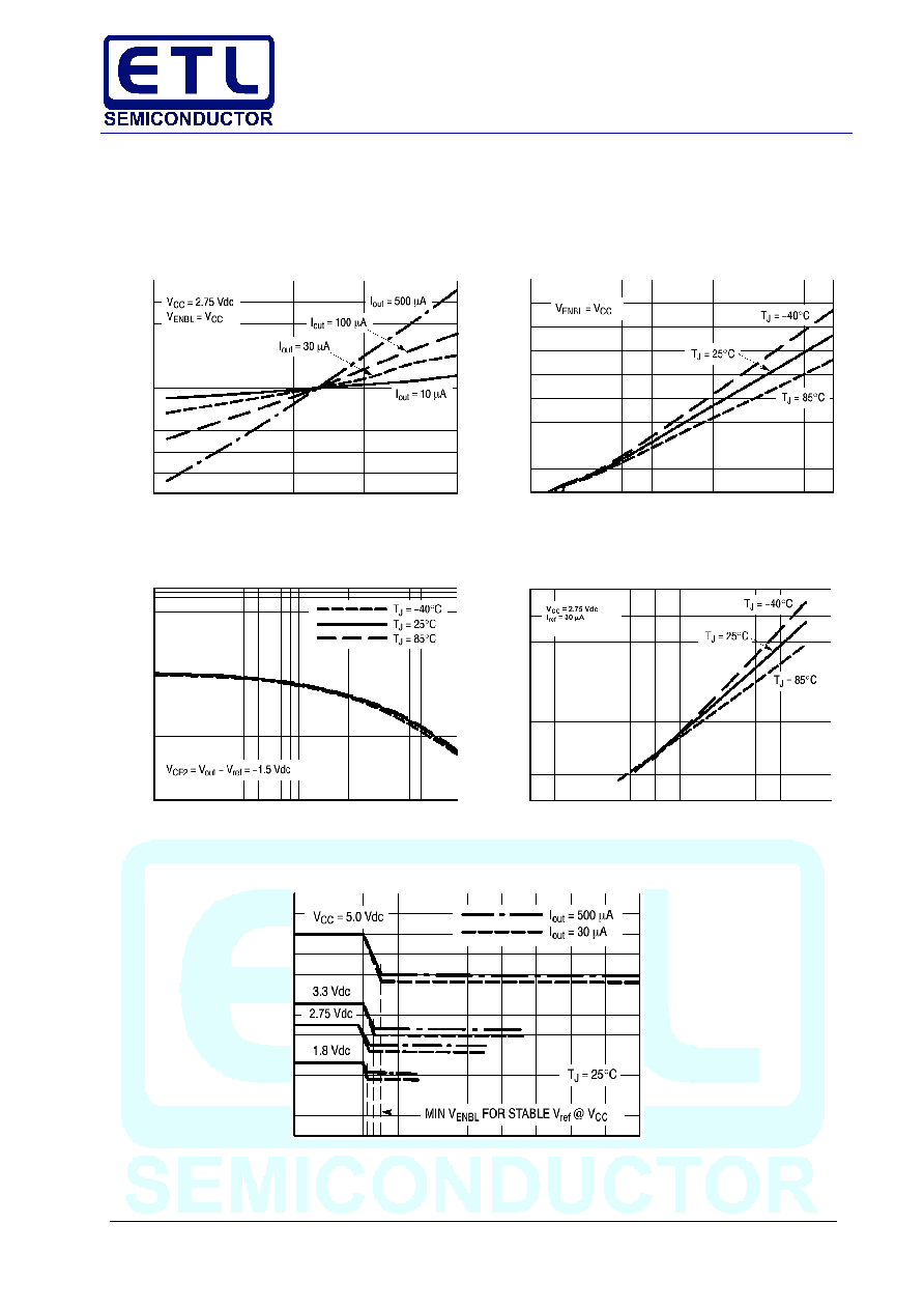
TYPICAL OPEN LOOP CHARACTERISTICS
(Refer to Circuits of Figures 10 through 15)
T
J
, JUNCTION TEMPERATURE (∞C)
Figure 2.
V
ref
versus T
J
@ I
out
I
CC
, SUPPL
Y
CURRENT
(
µ
Adc)
I
ENABLE
(
µ
Adc)
V
CC
, SUPPLY VOLTAGE (V
dc
)
Figure 3. I
CC
versus V
CC
@ T
J
I
out
, DC OUTPUT CURRENT (
µ
Adc)
Figure 4. Q2 Current Gain versus Output Current @ T
J
V
ENABLE
(V
dc
)
Figure 5. I enable versus V enable
V
ENABLE
(V
dc
)
Figure 6. V ref versus V enable @ V CC and I out
V
ref
(mA)
V
ref
(Vdc)
H
FE
, Q2 DC CURRENT GAIN
-45 -35
-25
-15
-5
5
15
25
35
45
55
65
75
85
0
1
2
3
4
5
6
7
8
9
10
50
40
30
20
10
0
-10
-20
-30
-40
-50
900
800
700
600
500
400
300
200
100
0
10
20
30
50
100
200
300
500
1000
1000
500
300
200
100
50
30
20
10
0
0.5
1.0
1.5
2.0
2.5
3.0
160
140
120
100
80
60
40
20
0
0
0.5
1.0
1.5
2.0
2.5
3.0
3.5
4.0
4.5
5.0
6.0
5.0
4.0
3.0
2.0
1.0
0
