 | –≠–ª–µ–∫—Ç—Ä–æ–Ω–Ω—ã–π –∫–æ–º–ø–æ–Ω–µ–Ω—Ç: MSQA6V1W5 | –°–∫–∞—á–∞—Ç—å:  PDF PDF  ZIP ZIP |
MSQA6V≠1/3
1
3
2
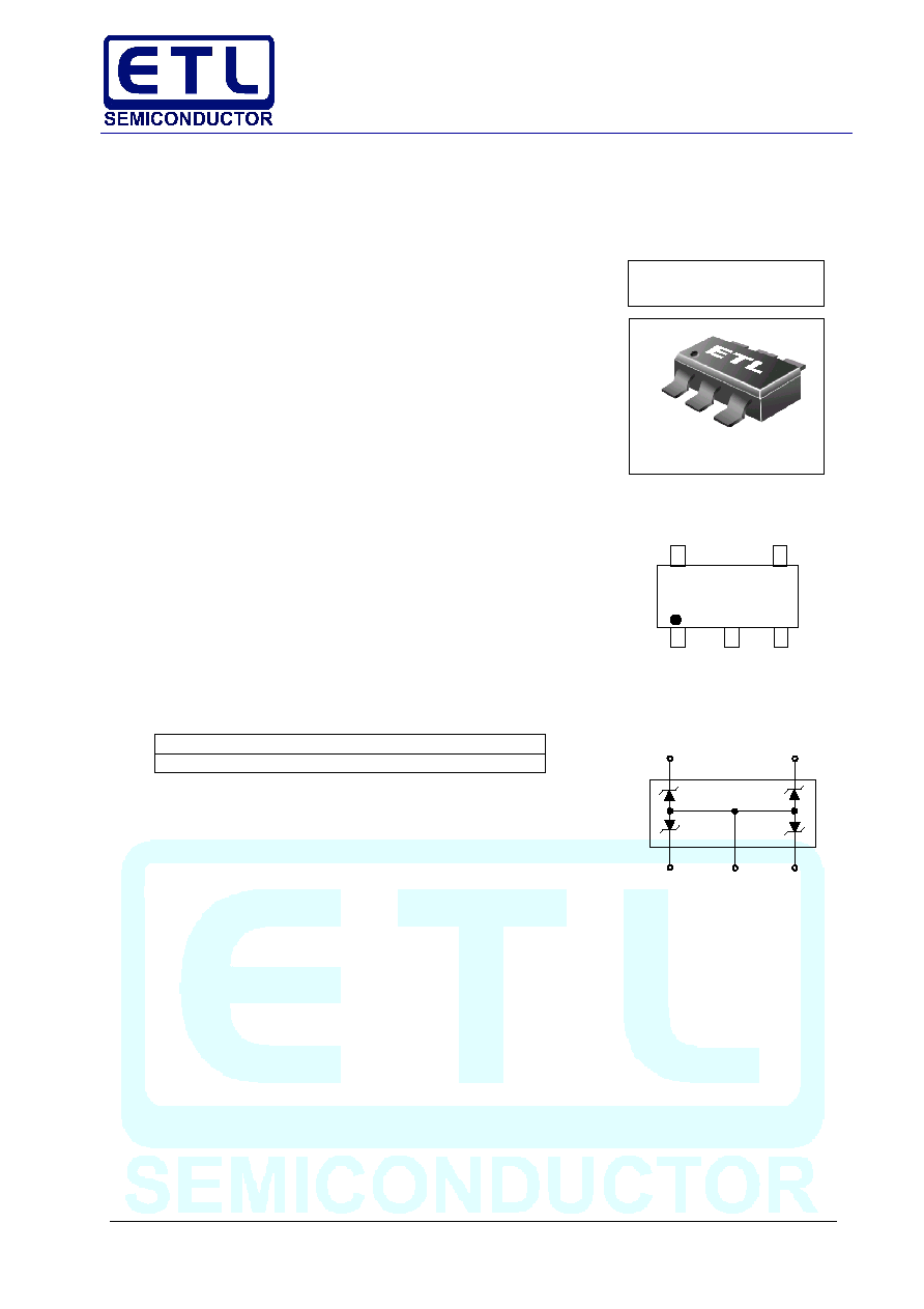
MSQA6V1W5
SOT-353 /SC-88A
CASE 419A
4
5
Quad Array for ESD Protection
This quad monolithic silicon voltage suppressor is designed for applications
requiring transient overvoltage protection capability. It is intended for use in volt-
age and ESD sensitive equipment such as computers, printers, business
machines, communication systems, medical equipment, and other applications.
Its quad junction common anode design protects four separate lines using only
one package. These devices are ideal for situations where board space is at a
premium.
Specification Features
∑ SC88A Package Allows Four Separate Unidirectional Configurations
∑ Low Leakage < 1
µ
A @ 3 Volt
∑ Breakdown Voltage: 6.1 Volt ≠ 7.2 Volt @ 1 mA
∑ Low Capacitance (90 pF typical)
∑ ESD Protection Meeting IEC1000≠4≠2
Mechanical Characteristics
∑ Void Free, Transfer≠Molded, Thermosetting Plastic Case
∑ Corrosion Resistant Finish, Easily Solderable
∑ Package Designed for Optimal Automated Board Assembly
∑ Small Package Size for High Density Applications
61 = Device Marking
D = One Digit Date Code
MARKING DIAGRAM
61
1
2
3
4
5
D
1
3
2
5
4
ORDERING INFORMATION
Device
Package
Shipping
MSQA6V1W5
SC≠88A
3000/Tape & Reel
MSQA6V≠2/3
MAXIMUM RATINGS
(T
A
= 25∞C unless otherwise noted)
Characteristic
Symbol
Value
Unit
Peak Power Dissipation @ 20
µ
s @T
A
< 25∞C (Note 1.)
P
pk
150
Watts
Steady State Power ≠ 1 Diode (Note 2.)
P
D
385
mW
Thermal Resistance Junction to Ambient
R
JA
325
∞C/W
Above 25∞C, Derate
3.1
mW/∞C
Maximum Junction Temperature
T
JMax
150
∞C
Operating Junction and Storage Temperature Range
T
J
,T
stg
≠55 to +150
∞C
ESD Discharge
MIL STD 883C ≠ Method 3015≠6
V
PP
16
kV
IEC1000≠4≠2, Air Discharge
16
IEC1000≠4≠2, Contact Discharge
9
Lead Solder Temperature (10 seconds duration)
T
L
260
∞C
ELECTRICAL CHARACTERISTICS
MSQA6V1W5
Breakdown Voltage
V
BR
@ 1 mA (Volts)
Leakage Current
I
RM
@ V
RM
= 3 V
Capacitance
@ 0 V Bias
Max
V
F
@ I
F
= 200 mA
Device
Min
Nom
Max
(
µµ
µµ
µ
A)
(pF)
(V)
MSQA6V1W5
6.1
6.6
7.2
1.0
90
1.25
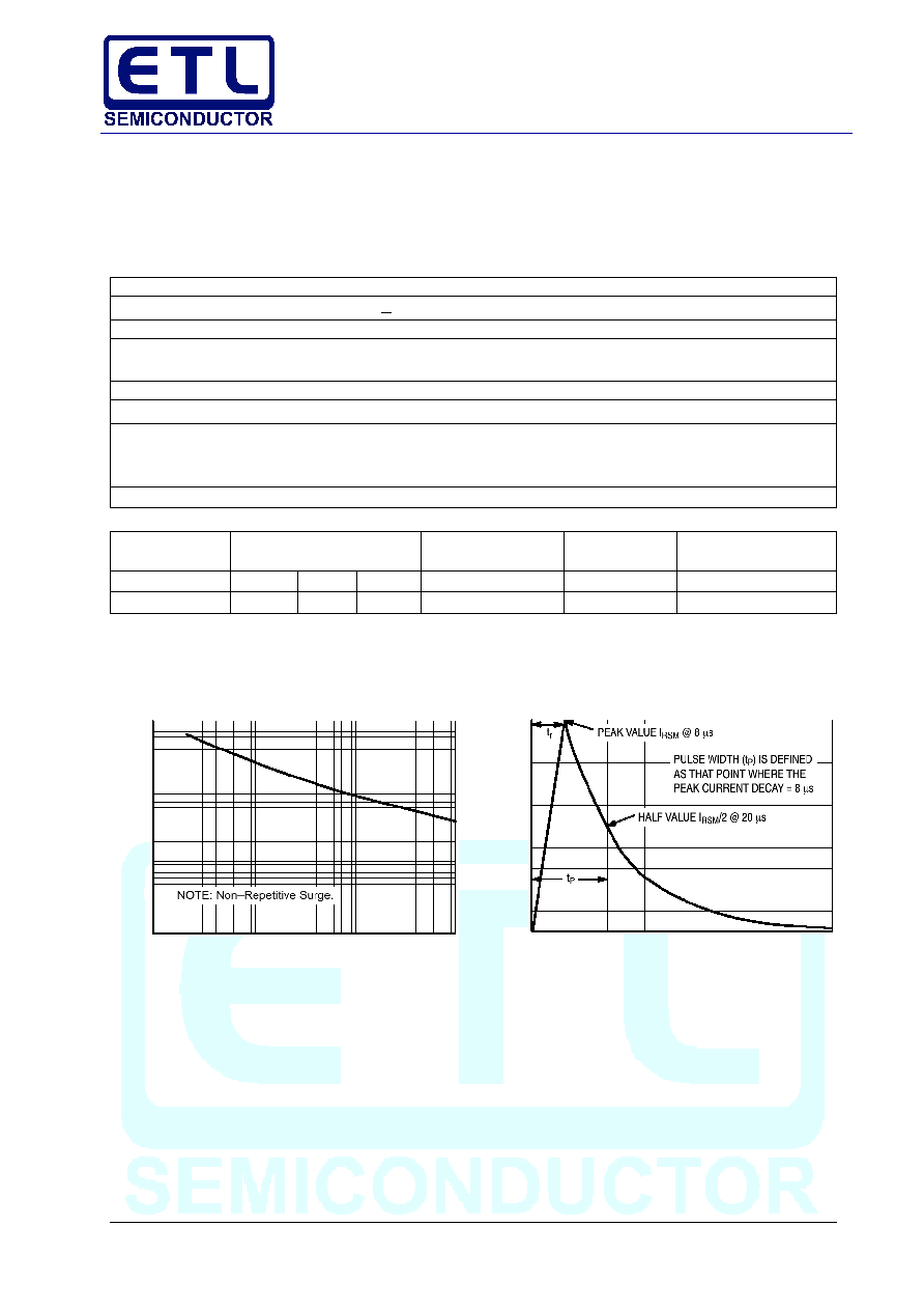
1. Non≠repetitive current per Figure 1. Derate per Figure 2.
2. Only 1 diode under power. For all 4 diodes under power, P
D
will be 25%. Mounted on FR≠4 board with min pad.
P
pk
, PEAK SURGE POWER (W
A
TTS)
t, TIME (ms)
Figure 1. Pulse Width
t, TIME (
µ
s)
Figure 2. 8
◊
20
µµ
µµ
µ
s Pulse Waveform
100
90
80
70
60
50
40
30
20
10
0
% OF PEAK PULSE CURRENT
0
20
40
60
80
1000
100
100
1
1
10
100
1000
MSQA6V≠3/3
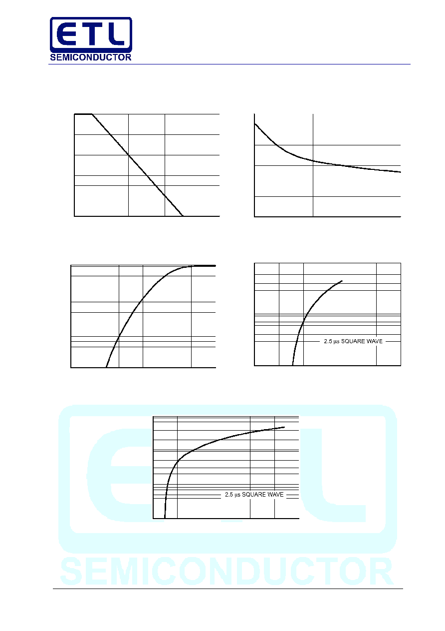
0
25
50
75
100
125
150
175
200
0
1.0
2.0
3.0
4.0
5.0
100
90
80
70
60
50
40
30
20
10
0
TYPICAL
CAP
ACIT
ANCE (pF)
1 MHz FREQUENCY
0.6
0.7
0.8
0.9
1.0
1.0
1.2
1.0
0.1
0.01
0.001
I pp, PEAK PULSE CURRENT (AMPS)
100
10
1.0
0
5.0
10
15
20
25
30
I
F
, FOR
W
ARD CURRENT
(A)
MSQA6V1W5
T
A
, AMBIENT TEMPERATURE (∞C)
Figure 3. Pulse Derating Curve
BIAS VOLTAGE (VOLTS)
Figure 4. Capacitance
V
F
, FORWARD VOLTAGE (VOLTS)
Figure 5. Forward Voltage
V
C
, CLAMPING VOLTAGE (VOLTS)
Figure 6. Clamping Voltage versus Peak
Pulse Current (Reverse Direction)
OR CURRENT
@
T
A
= 25 C ∞
V
C
, FORWARD CLAMPING VOLTAGE (VOLTS)
Figure 7. Clamping Voltage versus Peak
Pulse Current (Forward Direction)
I pp , PEAK FOR
W
ARD
PULSE CURRENT (AMPS)
100
90
80
70
60
50
40
30
20
10
0
0
2.0
4.0
6.0
8.0
10
12
100
10
1.0
0.1