
EtronTech
EM639165
Etron Technology, Inc.
No. 6, Technology Rd. V, Science-Based Industrial Park, Hsinchu, Taiwan 30077, R.O.C.
TEL: (886)-3-5782345
FAX: (886)-3-5778671
Etron Technology, Inc., reserves the right to make changes to its products and specifications without notice.
8Mega x 16bits SDRAM
Preliminary (Rev 1.0, 2/2001)
Features
∑
Single 3.3
±
0.3V power supply
∑
Fast clock rate
-
PC133: 133 MHz (CL3)
-
PC100: 100 MHz (CL2)
∑
Fully synchronous operation referenced to clock
rising edge
∑
4-bank operation controlled by BA0, BA1 (Bank
Address)
∑
Programmable Mode registers
- /CAS Latency: 2 or 3
- Burst Length: 1, 2, 4, 8 or full page
- Burst Type: interleaved or linear burst
∑
Byte Control ≠ DQML and DQMU
∑
Random column access
∑
Auto precharge / All banks precharge controlled
by A10
∑
Auto and self-refresh
∑
Self-refresh mode: standard and low power
∑
4096 refresh cycles/64ms
∑
Interface: LVTTL
∑
54-pin 400 mil plastic TSOP II package
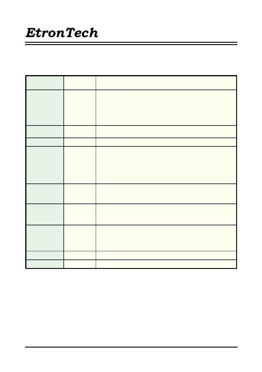
Key Specifications
EM639165
-
75/8
t
CK2
Clock Cycle time (min., CL=2)
10/10 ns
t
CK3
Clock Cycle time (min., CL=3)
7.5/8 ns
t
AC2
Access time (max., CL=2)
6/6 ns
t
AC3
Access time (max., CL=3)
5.4/6 ns
t
RAS
Row Active time (max.)
45/48 ns
t
RC
Row Cycle time(min.)
67.5/70 ns
Overview
EM639165 is a high-speed Synchronous Dynamic
Random Access Memory (SDRAM), organized as 4
banks x 2,097,152 words x 16 bits. All inputs and
outputs are referenced to the rising edge of CLK.
It achieves very high-speed data rates up to
133MHz, and is suitable for main memories or graphic
memories in computer systems. For handheld device
application, we also provide a low power option, with
self-refresh current under 800
µ
A.
Pin Assignment (Top View)
Ordering Information
Part Number
Speed
Grade
Self refresh
current (Max.)
EM639165TS-75
PC133/CL3
2 mA
EM639165TS-75L
PC133/CL3
800
µ
A
EM639165TS-8
PC100/CL2
2 mA
EM639165TS-8L
PC100/CL2
800
µ
A
V D D
D Q 0
V D D Q
D Q 1
D Q 2
V S S Q
D Q 3
D Q 4
V D D Q
D Q 5
D Q 6
V S S Q
D Q 7
V D D
D Q M L
/WE
/ C A S
/ R A S
/CS
B A 0
B A 1
A 1 0 ( A P )
A 0
A 1
A 2
A 3
V D D
1
2
3
4
5
6
7
8
9
1 0
1 1
1 2
1 3
1 4
1 5
1 6
1 7
1 8
1 9
2 0
2 1
2 2
2 3
2 4
2 5
2 6
2 7
5 4
5 3
5 2
5 1
5 0
4 9
4 8
4 7
4 6
4 5
4 4
4 3
4 2
4 1
4 0
3 9
3 8
3 7
3 6
3 5
3 4
3 3
3 2
3 1
3 0
2 9
2 8
V S S
D Q 1 5
V S S Q
D Q 1 4
D Q 1 3
V D D Q
D Q 1 2
D Q 1 1
V S S Q
D Q 1 0
D Q 9
V D D Q
D Q 8
V S S
N C
D Q M U
C L K
C K E
N C
A 1 1
A 9
A 8
A 7
A 6
A 5
A 4
V S S
EM639165
Preliminary
Rev 1.0 Feb. 2001
2
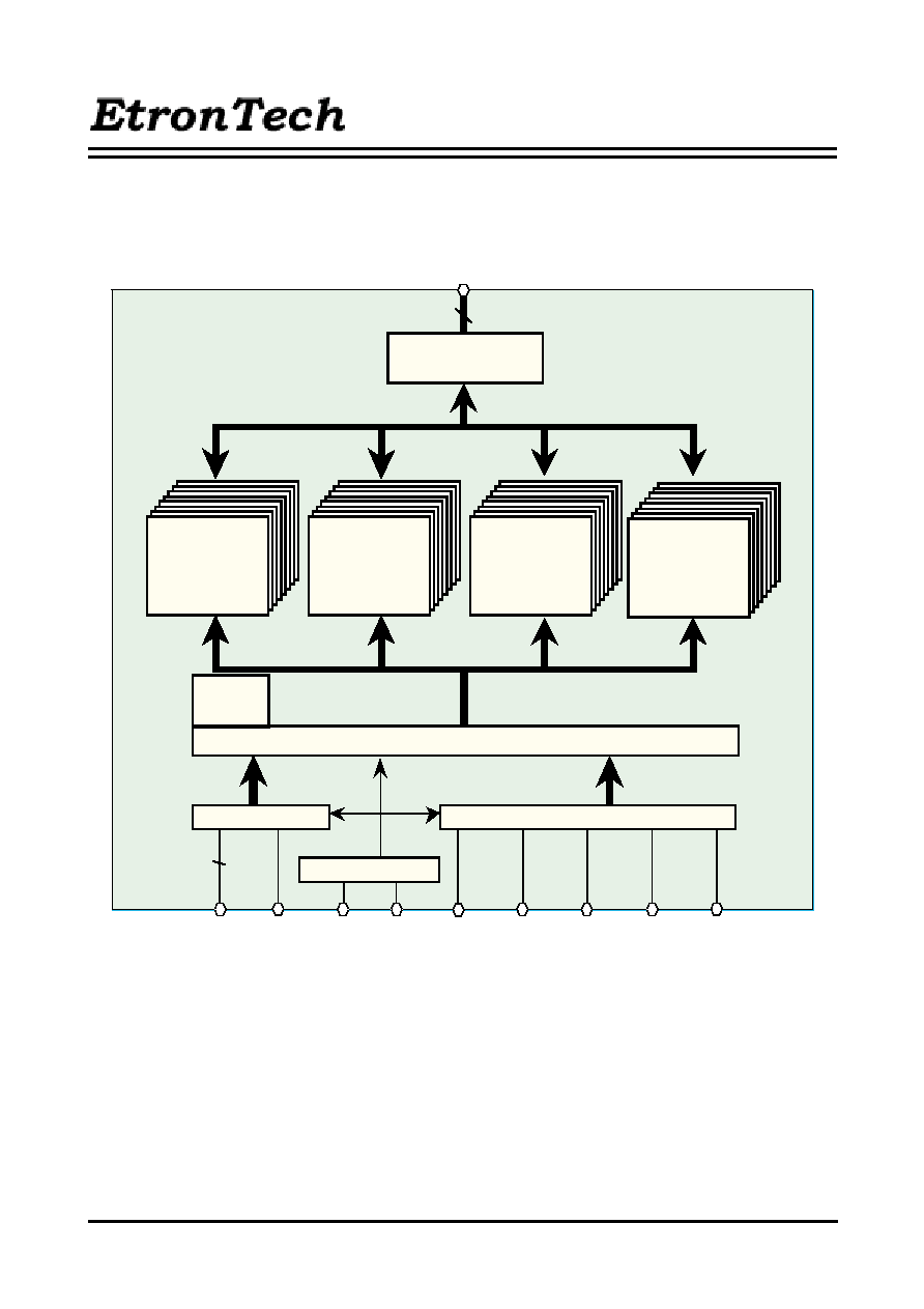
BLOCK DIAGRAM
Address Buffer
A0-11
BA0,1
Control Signal Buffer
/CS
/RAS
/CAS
/WE
CLK
CKE
Clock Buffer
Control Circuitry
I/O Buffer
DQ0-15
Mode
Register
DQM
Memory Array
Bank #0
4096 x512x16
Cell Array
Memory Array
Bank #1
Cell Array
Memory Array
Bank #2
Cell Array
Memory Array
Bank #3
Cell Array
4096 x512x16
4096 x512x16
4096 x512x16
Preliminary
Rev 1.0 Feb. 2001
EM639165
3
PIN FUNCTION
CLK
Input
Master Clock:
All other inputs are referenced to the rising edge of CLK
CKE
Input
Clock Enable:
CKE controls internal clock.When CKE is low, internal clock for
the following cycle is ceased. CKE is also used to select
auto / self-refresh.
After self-refresh mode is started, CKE becomes asynchronous input.
Self-refresh is maintained as long as CKE is low.
/CS
Input
Chip Select:
When /CS is high, any command means No Operation.
/RAS, /CAS, /WE
Input
Combination of /RAS, /CAS, /WE defines basic commands.
A0-11
Input
A0-11 specify the Row / Column Address in conjunction with BA0,1.
The Row Address is specified by A0-11.
The Column Address is specified byA0-8.
A10 is also used to indicate precharge option. When A10 is high at a
read / write command, an auto precharge is performed. When A10 is
high at a precharge command, all banks are precharged.
BA0,1
Input
Bank Address:
BA0,1 specifies one of four banks to which a command is applied.
BA0,1 must be set with ACT, PRE , READ , WRITE commands.
Input / Output
Input
Din Mask / Output Disable:
When DQM(U/L) is high in burst write, Din for the current cycle is
masked. When DQM(U/L) is high in burst read,
Dout is disabled at the next but one cycle.
VDD,VSS
Power Supply
Power Supply for the memory array and peripheral circuitry.
VDDQ,VSSQ
Power Supply
VDDQ and VSSQ are supplied to the Output Buffers only.
Data In and Data out are referenced to the rising edge of CLK.
DQ0-15
DQMU/L
EM639165
Preliminary
Rev 1.0 Feb. 2001
4
Activate (ACT) [/RAS =L, /CAS =/WE =H]
ACT command activates a row in an idle bank indicated by BA.
Read (READ) [/RAS =H, /CAS =L, /WE =H]
READ command starts burst read from the active bank indicated by BA. First output
data appears after /CAS latency. When A10 =H at this command, the bank is deac-
tivated after the burst read (auto-precharge, READA).
Write (WRITE) [/RAS =H, /CAS =/WE =L]
WRITE command starts burst write to the active bank indicated by BA. Total data
length to be written is set by burst length. When A10 =H at this command, the bank
is deactivated after the burst write (auto-precharge, WRITEA).
Precharge (PRE) [/RAS =L, /CAS =H, /WE =L]
PRE command deactivates the active bank indicated by BA. This command also
terminates burst read / write operation. When A10 =H at this command, all banks
are deactivated (precharge all, PREA ).
Auto-Refresh (REFA) [/RAS =/CAS =L, /WE =CKE =H]
REFA command starts auto-refresh cycle. Refresh address including bank address
are generated internally. After this command, the banks are precharged automatically.
BASIC FUNCTIONS
The EM639165 provides basic functions, bank (row)
activate, burst read / write, bank (row) precharge, and auto
/ self refresh.
Each command is defined by control signals of /RAS, /CAS
and /WE at CLK rising edge. In addition to 3 signals, /CS
,CKE and A10 are used as chip select, refresh opt ion, and
precharge option, respectively .
To know the detailed definition of commands, please see
the command truth table.
/CS
Chip Select : L=select, H=deselect
/RAS
Command
/CAS
Command
/WE
Command
CKE
Refresh Option @ refresh command
A10
Precharge Option @ precharge or read/write command
CLK
define basic command

Preliminary
Rev 1.0 Feb. 2001
EM639165
5
H=High Level, L=Low Level, V=Valid, X=Don't Care, n=CLK cycle number
NOTE: 1. A7-A9 =0, A0-A6 =Mode Address
COMMAND TRUTH TABLE
COMMAND
MNEMONIC
CKE
n-1
CKE
n
/CS
/RAS /CAS
/WE
BA0,1 A1 1
A1 0
A0-9
DESEL
H
X
H
X
X
X
X
X
X
X
No Operation
NOP
H
X
L
H
H
H
X
X
X
X
ACT
H
X
L
L
H
H
V
V
V
V
PRE
H
X
L
L
H
L
V
X
L
X
PREA
H
X
L
L
H
L
X
H
X
WRIT E
H
X
L
H
L
L
V
V
L
V
WRITE A
H
X
L
H
L
L
V
V
H
V
READ
H
X
L
H
L
H
V
V
L
V
READA
H
X
L
H
L
H
V
V
H
V
Auto-Refresh
REFA
H
H
L
L
L
H
X
X
X
X
Self-Refresh Entry
REFS
H
L
L
L
L
H
X
X
X
X
Self-Refresh Exit
REFSX
L
H
H
X
X
X
X
X
X
X
L
H
L
H
H
H
X
X
X
X
Mode Register Set
MRS
H
X
L
L
L
L
L
L
L
V*1
X
Burst Terminate
TBST
H
X
L
H
H
L
X
X
X
X
Deselect
Row Address Entry &
Bank Active
Single Bank Precharge
Precharge All Banks
Column Address Entry
&Write
Column Address Entry &
Write with Auto-Precharge
Column Address Entry
& Read
Column Address Entry &
Read with Auto-Precharge