Et r onT ech
EM6A9320
Etron Technology, Inc.
No. 6, Technology Rd. V, Science-Based Industrial Park, Hsinchu, Taiwan 30077, R.O.C.
TEL: (886)-3-5782345
FAX: (886)-3-5778671
Etron Technology, Inc., reserves the right to make changes to its products and specifications without notice.
4M x 32 DDR SDRAM
Etron Confidential
Preliminary (Rev 0.3 7/2002)
Features
∑
Fast clock rate: 350/333/300/285/250/200 MHz
∑
Differential Clock CK & CK# input
∑
4 Bi-directional DQS. Data transactions on both
edges of DQS (1DQS / Byte)
∑
DLL aligns DQ and DQS transitions
∑
Edge aligned data & DQS output
∑
Center aligned data & DQS input
∑
4 internal banks, 1M x 32-bit for each bank
∑
Programmable mode and extended mode registers
- CAS# Latency: 3, 4, 5
- Burst length: 2, 4, 8
- Burst Type: Sequential & Interleave
∑
Full page burst length for sequential type only
∑
Start address of full page burst should be even
∑
All inputs except DQ's & DM are at the positive
edge of the system clock
∑
No Write-Interrupted by Read function
∑
4 individual DM control for write masking only
∑
Auto Refresh and Self Refresh
∑
4096 refresh cycles / 32ms
∑
Power supplies up to 350/333/300/285MHz:
V
DD
= 2.8V
±
5%
V
DDQ
= 2.8V
±
5%
∑
Power supplies up to 250/200MHz:
V
DD
= 2.5V
±
5%
V
DDQ
= 2.5V
±
5%
∑
Interface : SSTL_2 I/O compatible
∑
6WDQGDUG EDOO )%*$ SDFNDJH
Overview
The EM6A9320 DDR SDRAM is a high-speed CMOS
double data rate synchronous DRAM containing 128
Mbits. It is internally configured as a quad 1M x 32
DRAM with a synchronous interface (all signals are
registered on the positive edge of the clock signal, CK).
Data outputs occur at both rising edges of CK and CK#.
Read and write accesses to the SDRAM are burst
oriented; accesses start at a selected location and
continue for a programmed number of locations in a
programmed sequence.
Accesses begin with the registration of a BankActivate
command, which is then followed by a Read or Write
command.
The EM6A9320 provides programmable Read or Write
burst lengths of 2, 4, 8. An auto precharge function may
be enabled to provide a self-timed row precharge that is
initiated at the end of the burst sequence.
The refresh functions, either Auto or Self Refresh are
easy to use.
In addition, EM6A9320 features programmable DLL
option. By having a programmable mode register and
extended mode register, the system can choose the
most suitable modes to maximize its performance.
These devices are well suited for applications requiring
high memory bandwidth, result in a device particularly
well suited to high performance main memory and
graphics applications.
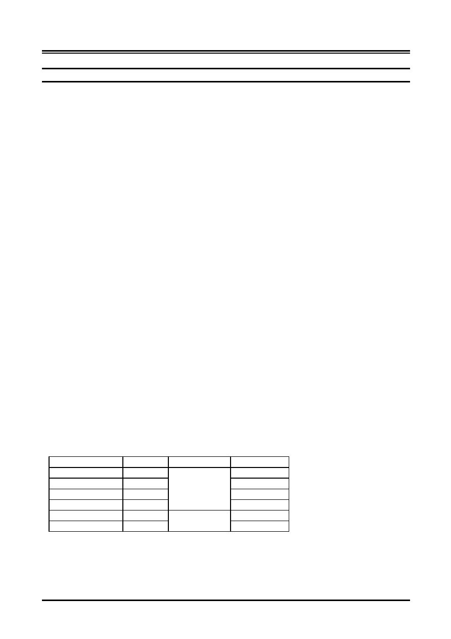
Ordering Information
Part Number
Frequency
Power Supply
Package
EM6A9320BI-2.8 350MHz
FBGA
EM6A9320BI-3.0 333MHz
FBGA
EM6A9320BI-3.3 300MHz
FBGA
EM6A9320BI-3.5 285MHz
V
DD
2.8V
V
DDQ
2.8V
FBGA
EM6A9320BI-4 250MHz
FBGA
EM6A9320BI-5 200MHz
V
DD
2.5V
V
DDQ
2.5V
FBGA

Et r onT ech
4Mx32 DDR SDRAM
EM6A9320
Etron Confidential
2
Rev 0.3
July. 2002
Pin Assignment (FBGA 144Ball Top View)
Pin Assignment by Name (FBGA 144Ball)
Symbol Location Symbol Location Symbol Location Symbol Location Symbol Location Symbol Location Symbol Location Symbol Location
A0 M4 DQ6 C1 DQ24
D12 CK L10
VDDQ B6 VSS E5 VSS J7 VSSQ G4
A1 M5 DQ7 D1 DQ25
C12 CK# L11
VDDQ B7 VSS E6 VSS J8 VSSQ G9
A2 L5 DQ8 J12
DQ26
C11 CKE M11
VDDQ B9 VSS E7 VSS K4 VSSQ H4
A3 M6 DQ9 J11 DQ27 B12 CS# M1 VDDQ B11 VSS E8 VSS K9 VSSQ H9
A4 M7 DQ10 H12 DQ28 A9 RAS# L1 VDDQ D2 VSS F5 VSSQ A3
VSSQ J4
A5 L8 DQ11 H11 DQ29 A8 CAS# K1 VDDQ D11 VSS F6 VSSQ A10 VSSQ J9
A6
M8
DQ12
F12
DQ30
B8
WE#
K2
VDDQ
E3
VSS
F7
VSSQ
C3
NC B3
A7
M9
DQ13
F11
DQ31
A7
VREF M12 VDDQ E10
VSS
F8
VSSQ
C4
NC B10
A8/AP M10 DQ14
E12 DQS0
A1
VDD
C6
VDDQ
F3
VSS
G5
VSSQ
C5
NC G3
A9
L7
DQ15
E11 DQS1 G12
VDD
C7
VDDQ F10
VSS
G6
VSSQ
C8
NC G10
A10
K5
DQ16
E2
DQS2
G1
VDD
D3
VDDQ
H3
VSS
G7
VSSQ
C9
NC K8
A11
L6
DQ17
E1
DQS3
A12
VDD
D10 VDDQ H10
VSS
G8
VSSQ C10
NC K11
DQ0
A6
DQ18
F2
DM0
A2
VDD
K3
VDDQ
J3
VSS
H5
VSSQ
D5
NC K12
DQ1
B5
DQ19
F1
DM1
G11
VDD
K6
VDDQ J10
VSS
H6
VSSQ
D8
NC L2
DQ2
A5
DQ20
H2
DM2
G2
VDD
K7
VSS
D4
VSS
H7
VSSQ
E4
NC L3
DQ3
A4
DQ21
H1
DM3
A11
VDD
K10
VSS
D6
VSS
H8
VSSQ
E9
NC L9
DQ4
B1
DQ22
J1
BA0
M3
VDDQ
B2
VSS
D7
VSS
J5
VSSQ
F4
NC L12
DQ5 C2 DQ23 J2 BA1 L4 VDDQ B4 VSS D9 VSS J6 VSSQ F9 NC M2
12
11
10
9
8
7
6
5
4
3
2
1
M
L
K
J
H
G
F
E
D
C
B
A
DQS0
DM0
DQ4
VDDQ
VSSQ
DQ3
NC
VDDQ
DQ6
DQ5
DQ7
VDDQ
VSSQ
VSSQ
VDD
VSS
DQ2
DQ0
DQ1
VDDQ
DQ31
DQ29
VDDQ
DQ30
VSSQ
VDD
VSSQ
VSS
VDD
VSSQ
VSS
VSSQ
DQ28
VSSQ
VDDQ
NC
DM3
DQS3
VDDQ
DQ27
VSSQ
VSSQ
VSS
VDD
DQ26
DQ25
VDDQ
DQ24
DQ17
DQ16
DQ19
DQ18
VDDQ
VSSQ
VDDQ
VSSQ
DQS2
DM2
DQ21
DQ20
NC
VSSQ
VDDQ
VSSQ
VSS
Thermal
VSS
Thermal
VSS
Thermal
VSS
Thermal
VSS
Thermal
VSS
Thermal
VSS
Thermal
VSS
Thermal
VSS
Thermal
VSS
Thermal
VSS
Thermal
VSS
Thermal
VSS
Thermal
VSS
Thermal
VSS
Thermal
VSS
Thermal
VSSQ
VDDQ
VSSQ
VDDQ
DQ15
DQ14
DQ13
DQ12
VSSQ
NC
VSSQ
VDDQ
DM1
DQS1
DQ11
DQ10
DQ22
DQ23
CAS#
WE#
VDDQ
VSSQ
VDD
VSS
RAS#
NC
CS#
NC
NC
BA1
BA0
A0
VSS
VSS
A10
VDD
VSS
VSS
VDD
NC
A2
A11
A1
A3
A9
A5
A4
A6
VSSQ
VDDQ
VSS
VDD
DQ9
DQ8
NC
NC
NC
CK
A7
A8/
AP
CK#
NC
CKE
VREF
Et r onT ech
4Mx32 DDR SDRAM
EM6A9320
Etron Confidential
3
Rev 0.3
July. 2002
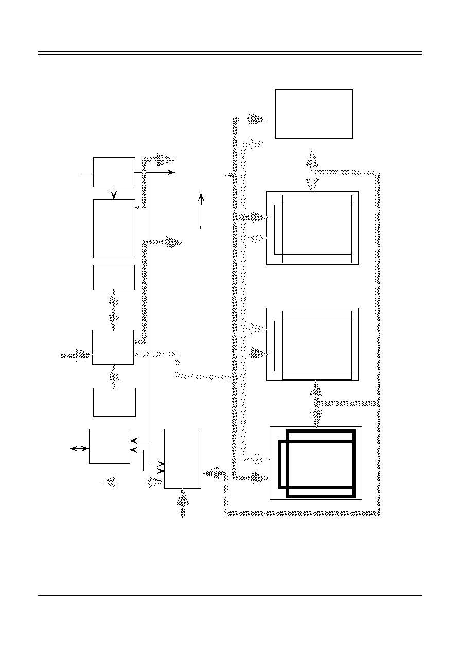
Block Diagram
SFGSFTI
DPVO
UFS
COLUMN
COUNTER
ADDRESS
BUFFER
A0
A10
A11
BA0
BA1
CONTROL
SIGNAL
GENERATOR
DM0~3
DLL
CLOCK
BUFFER
COMMAND
DECODER
Column Decoder
Sense Amplifier
Row
Decoder
4096 X 256 X 32
CELL ARRAY
(BANK #0)
Sense Amplifier
Column Decoder
Row
Decoder
4096 X 256 X 32
CELL ARRAY
(BANK #3)
MODE
REGISTER
CK
CK#
CKE
CS#
RAS#
CAS#
WE#
A8/AP
DQ0
D
DQ31
Sense Amplifier
Column Decoder
Row Decoder
4096 X 256 X 32
CELL ARRAY
(BANK #1)
Sense Amplifier
Column Decoder
Row Decoder
4096 X 256 X 32
CELL ARRAY
(BANK #2)
DQS0~3
DATA
STROBE
BUFFER
DQ
BUFFER

Et r onT ech
4Mx32 DDR SDRAM
EM6A9320
Etron Confidential
4
Rev 0.3
July. 2002
Pin Descriptions
Table 1. Pin Details of EM6A9320
Symbol Type
Description
CK, CK#
Input
Differential Clock: CK, CK# are driven by the system clock. All SDRAM input
commands are sampled on the positive edge of CK. Both CK and CK# increment the
internal burst counter and controls the output registers.
CKE Input
Clock Enable: CKE activates (HIGH) and deactivates (LOW) the CK signal. If CKE
goes low synchronously with clock, the internal clock is suspended from the next clock
cycle and the state of output and burst address is frozen as long as the CKE remains
low. When all banks are in the idle state, deactivating the clock controls the entry to
the Power Down and Self Refresh modes.
BA0, BA1
Input
Bank Select: BA0 and BA1 defines to which bank the BankActivate, Read, Write, or
BankPrecharge command is being applied. They also define which Mode Register or
Extended Mode Register is loaded during a Mode Register Set command.
A0-A11 Input
Address Inputs: A0-A11 are sampled during the Bank Activate command (row
address A0-A11) and Read/Write command (column address A0-A7 with A8 defining
Auto Precharge) to select one location out of the 256K available in the respective
bank. During a Precharge command, A8 is sampled to determine if all banks are to be
precharged (A8 = HIGH). The address inputs also provide the op-code during a Mode
Register Set or Extended Mode Register Set command.
CS# Input
Chip Select: CS# enables (sampled LOW) and disables (sampled HIGH) the
command decoder. All commands are masked when CS# is sampled HIGH. CS#
provides for external bank selection on systems with multiple banks. It is considered
part of the command code.
RAS# Input
Row Address Strobe: The RAS# signal defines the operation commands in
conjunction with the CAS# and WE# signals and is latched at the positive edges of
CK. When RAS# and CS# are asserted "LOW" and CAS# is asserted "HIGH" either
the BankActivate command or the Precharge command is selected by the WE# signal.
When the WE# is asserted "HIGH," the BankActivate command is selected and the
bank designated by BS is turned on to the active state. When the WE# is asserted
"LOW," the Precharge command is selected and the bank designated by BS is
switched to the idle state after the precharge operation.
CAS#
Input
Column Address Strobe: The CAS# signal defines the operation commands in
conjunction with the RAS# and WE# signals and is latched at the positive edges of
CK. When RAS# is held "HIGH" and CS# is asserted "LOW" the column access is
started by asserting CAS# "LOW" Then, the Read or Write command is selected by
asserting WE# "HIGH " or "LOW".
WE# Input
Write Enable: The WE# signal defines the operation commands in conjunction with
the RAS# and CAS# signals and is latched at the positive edges of CK. The WE#
input is used to select the BankActivate or Precharge command and Read or Write
command.
DQS0-DQS3
Input /
Output
Bidirectional Data Strobe: The DQSx signals are mapped to the following data
bytes: DQS0 to DQ0-DQ7, DQS1 to DQ8-DQ15, DQS2 to DQ16-DQ23, DQS3 to
DQ24-DQ31.
DM0 - DM3
Input
Data Input Mask: DM0-DM3 are byte specific. Input data is masked when DM is
sampled HIGH during a write cycle. DM3 masks DQ31-DQ24, DM2 masks DQ23-
DQ16, DM1 masks DQ15-DQ8, and DM0 masks DQ7-DQ0.
DQ0 - DQ31
Input /
Output
Data I/O: The DQ0-DQ31 input and output data are synchronized with the positive
edges of CK and CK#. The I/Os are byte-maskable during Writes.
V
DD
Supply
3RZHU 6XSSO\ 3RZHU IRU WKH LQSXW EXIIHUV DQG FRUH ORJLF
Et r onT ech
4Mx32 DDR SDRAM
EM6A9320
Etron Confidential
5
Rev 0.3
July. 2002
V
SS
Supply Ground: Ground
IRU WKH LQSXW EXIIHUV DQG FRUH ORJLF
V
DDQ
Supply DQ Power: Provide isolated power to DQs for improved noise immunity.
V
SSQ
Supply DQ Ground: Provide isolated ground to DQs for improved noise immunity.
V
REF
Supply Reference Voltage for Inputs: +0.5 x V
DDQ
NC -
No Connect: These pins should be left unconnected.
Note: The timing reference point for the differential clocking is the cross point of the CK and CK#. For any
applications using the single ended clocking, apply V
REF
to CK# pin.
Operation Mode
Fully synchronous operations are performed to latch the commands at the positive edges of CK . Table 2 shows
the truth table for the operation commands.
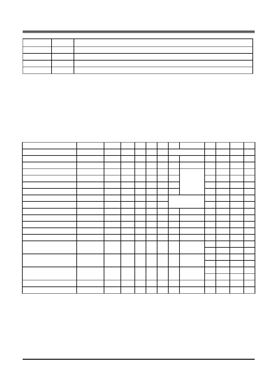
Table 2. Truth Table (Note (1), (2) )
Command State
CKEn-1 CKEn DM BA1 BA0 A8 A11-A9,
A7-0 CS# RAS# CAS# WE#
BankActivate Idle
(3)
H X X V V Row
Address L L H H
BankPrecharge
Any
H X X V V L
X
L L H L
PrechargeAll
Any
H X X X X H
X
L L H L
Write Active
(3)
H X V V V L
L H L L
Write and AutoPrecharge
Active
(3)
H X
V
V
V
H
L
H L
L
Read Active
(3)
H X X V V L
L H L H
Read and Autoprecharge
Active
(3)
H X X V V H
Column
Address
A0~A7
L H L H
Mode Register Set
Idle
H
X
X
L
L
L
L
L
L
Extended Mode Register Set
Idle H
X
X
L
H
OP code
L L L L
No-Operation
Any
H X X X X X
X
L H H H
Device
Deselect
Any
H X X X X X
X
H X X X
Burst Stop
Active
(4)
H X X X X X
X
L H H L
AutoRefresh
Idle
H H X X X X
X
L L L H
SelfRefresh
Entry
Idle
H
L X X X X
X
L L L H
H X X X
SelfRefresh Exit
Idle
(Self Refresh)
L
H X X X X
X
L H H H
H X X X
Power Down Mode Entry Idle/Active
(5)
H
L X X X X
X
L H H H
H X X X
Power Down Mode Exit
Any
(Power Down)
L
H X X X X
X
L H H H
Data Write/
Output Enable
Active
H X L X X X
X
X X X X
Data Mask/
Output Disable
Active
H X H X X X
X
X X X X
Note: 1. V = Valid data, X = Don't Care, L = Low level, H = High level
2. CKE
n
signal is input level when commands are provided.
CKE
n-1
signal is input level one clock cycle before the commands are provided.
3. These are states of bank designated by BA0, BA1signals.
4. Read burst stop with BST command for all burst types.
5. Power Down Mode can not enter in the burst operation.
When this command is asserted in the burst cycle, device state is clock suspend mode.