Features
∑ Low voltage of +3.3 V single power supply
∑ 6.5 k
high transimpedance
∑ Typical 320 MHz broad bandwidth
∑ 27 dB high gain
∑ 0 dBm large optical input
∑ Over 30 dB wide dynamic range
∑ Differential output
Applications
∑ Preamplifier of an optical receiver circuit for
OC-12/STM-4 (622 Mb/s)
Functional Description
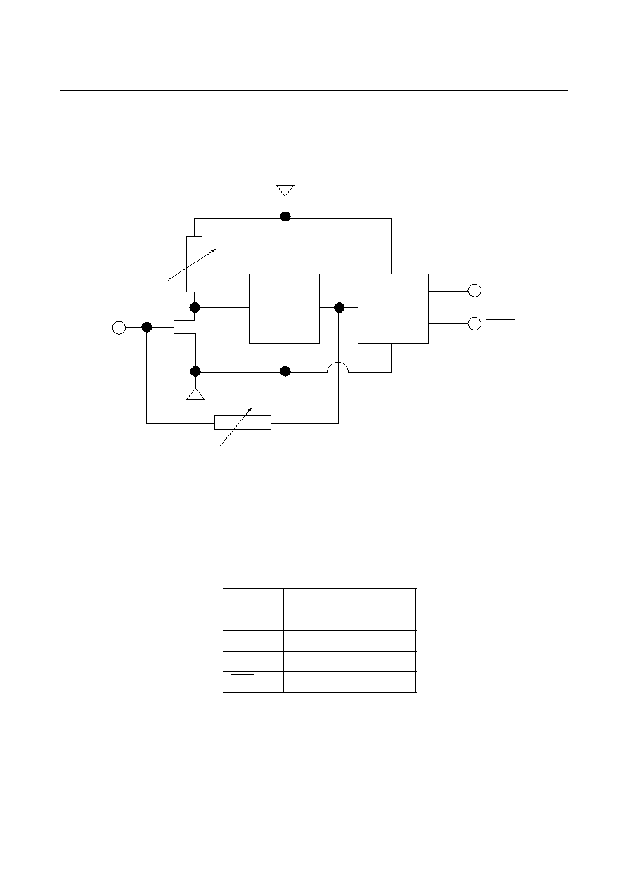
The F0100208B is a stable GaAs integrated transimpedance amplifier capable of 27 dB
gain at a typical 320 MHz 3 dB-cutoff-frequency, making it ideally suited for a 622 Mb/s
optical receiver circuit, for example, OC-12/STM-4, instrumentation, and measurement ap-
plications. The integrated feedback loop design provides broad bandwidth and stable opera-
tion. The F0100208B typically specifies a high transimpedance of 6.5 k
(Rs=RL=50
) with
a wide dynamic range of over 30 dB. It also provides a large optical input overload of more
than 0 dBm. Furthermore, it can operate with a low supply voltage of single +3.3 V. It features
a typical dissipation current of 25 mA.
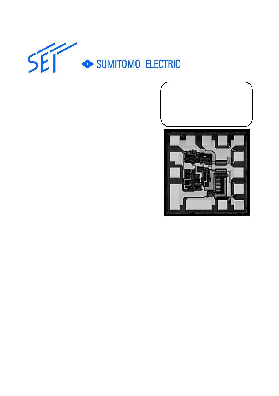
Only chip-shipment is available for all product lineups of GaAs transimpedance amplifi-
ers, because the packaged preamplifier can not operate with the maximum performance
owing to parasitic capacitance of the package.
01.08.28
Transimpedance Amplifier
F0100208B
3.3 V / 622 Mb/s Receiver

3.3 V / 622 Mb/s Transimpedance Amplifier
F0100208B
Absolute Maximum Ratings
T
a
=25
∞
C , unless specified
Recommended Operating Conditions
T
a
=25
∞
C , V
DD
=+3.3 V, V
SS
=GND, unless specified
Electrical Characteristics
T
a
=25
∞
C , V
DD
=3.3 V, V
SS
=GND, unless specified
*1 ZTP,N=
(R1+50)
2
◊
10
S21P,N
20
r
e
t
e
m
a
r
a
P
l
o
b
m
y
S
e
u
l
a
V
s
t
i
n
U
e
g
a
t
l
o
V
y
l
p
p
u
S
V
D
D
V
S
S
V
o
t
5
.
0
-
S
S
0
.
4
+
V
t
n
e
r
r
u
C
y
l
p
p
u
S
I
D
D
0
5
A
m
e
r
u
t
a
r
e
p
m
e
T
g
n
i
t
a
r
e
p
O
t
n
e
i
b
m
A
T
a
0
9
+
o
t
0
4
-
C
∞
e
r
u
t
a
r
e
p
m
e
T
e
g
a
r
o
t
S
T
g
t
s
5
2
1
+
o
t
0
5
-
C
∞
r
e
t
e
m
a
r
a
P
l
o
b
m
y
S
e
u
l
a
V
s
t
i
n
U
.
n
i
M
.
x
a
M
e
g
a
t
l
o
V
y
l
p
p
u
S
V
D
D
9
.
2
6
.
3
V
e
r
u
t
a
r
e
p
m
e
T
g
n
i
t
a
r
e
p
O
t
n
e
i
b
m
A
T
a
0
5
8
C
∞
r
e
t
e
m
a
r
a
P
l
o
b
m
y
S
s
n
o
i
t
i
d
n
o
C
t
s
e
T
e
u
l
a
V
s
t
i
n
U
.
n
i
M
.
p
y
T
.
x
a
M
t
n
e
r
r
u
C
y
l
p
p
u
S
I
D
D
C
D
8
1
5
3
5
4
A
m
)
e
v
i
t
i
s
o
P
(
n
i
a
G
S
P
1
2
,
z
H
M
1
=
f
m
B
d
0
5
-
=
N
I
P
0
5
=
L
R
7
2
5
.
8
2
2
3
B
d
)
e
v
i
t
a
g
e
n
(
n
i
a
G
S
N
1
2
,
z
H
M
1
=
f
m
B
d
0
5
-
=
N
I
P
0
5
=
L
R
7
2
5
.
8
2
2
3
B
d
f
f
o
-
t
u
C
y
c
n
e
u
q
e
r
F
h
g
i
H
B
d
3
-
)
e
v
i
t
i
s
o
p
(
F
P
C
0
5
=
L
R
m
B
d
0
5
-
=
N
I
P
5
6
2
0
4
3
0
0
6
z
H
M
f
f
o
-
t
u
C
y
c
n
e
u
q
e
r
F
h
g
i
H
B
d
3
-
)
e
v
i
t
a
g
e
n
(
F
N
C
0
5
=
L
R
m
B
d
0
5
-
=
N
I
P
5
6
2
0
2
3
0
0
6
z
H
M
e
c
n
a
d
e
p
m
I
t
u
p
n
I
R
I
z
H
M
1
=
f
0
5
3
0
5
4
0
5
5
)
e
v
i
t
i
s
o
p
(
e
c
n
a
d
e
p
m
I
-
s
n
a
r
T
Z
P
T
z
H
M
1
=
f
,
1
*
5
.
4
5
.
6
-
K
)
e
v
i
t
a
g
e
n
(
e
c
n
a
d
e
p
m
I
-
s
n
a
r
T
Z
N
T
z
H
M
1
=
f
,
1
*
5
.
4
5
.
6
-
K
)
e
v
i
t
i
s
o
p
(
e
g
a
t
l
o
V
t
u
p
t
u
O
V
P
O
C
D
5
.
1
4
.
2
9
.
2
V
)
e
v
i
t
a
g
e
n
(
e
g
a
t
l
o
V
t
u
p
t
u
O
V
N
O
C
D
5
.
1
4
.
2
9
.
2
V
e
g
a
t
l
o
V
t
u
p
n
I
V
I
C
D
5
6
.
0
8
8
.
0
5
0
.
1
V
F0100208B
3.3 V / 622 Mb/s Transimpedance Amplifier
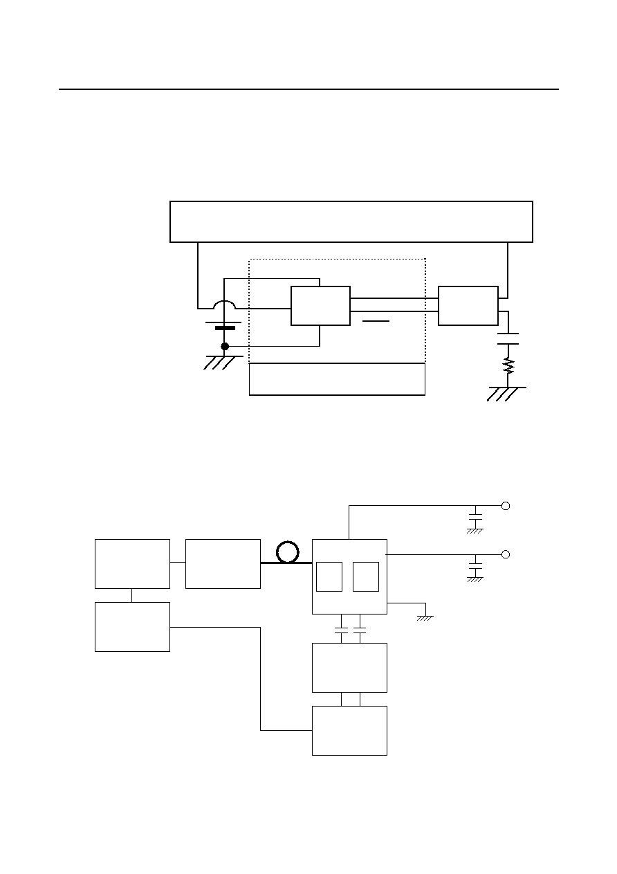
Test Circuits
1) AC Characteristics
2) Sensitivity Characteristics
E/O
Converter
Optical
Attenuater
Bit Error
Rate Tester
PD
Pulse
Pattern
Generator
Comparator
SEI
F0300232Q
V
PD
V
CC
5V
5V
CLK
0.022
µ
F
0.022
µ
F
0.022
µ
F
DUT
50
50
50
Network Analyzer
Prober
OUT
OUT
VDD
VSS
IN
DUT
Switch
Pin=-50 dBm
f=300 kHz~3 GHz