Features
∑
Low voltage of +5.0V single power supply
∑
1.5k
high transimpedance
∑
Typical 7.5GHz broad bandwidth
∑
29dB high gain
∑
Over 20dB wide dynamic range
∑
Differential output
Applications
∑
Preamplifier of an optical receiver circuit for OC-192/STM-64(10Gb/
s)
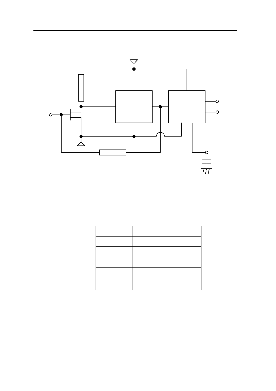
Functional Description
The F0100613B is a stable GaAs integrated transimpedance amplifier capable of 29dB
gain at a typical 7.5GHz 3dB-cutoff-frequency, making it ideally suited for a 10Gb/s optical
receiver circuit, for example, OC-192/STM-64, instrumentation, and measurement applica-
tions. The integrated feedback loop design provides broad bandwidth and stable operation.
The F0100613B typically specifies a high transimpedance of 1.5k
(RL=50
) with a wide
dynamic range of over 20dB. Furthermore, it can operate with a supply voltage of single
+5.0V.
Only chip-shipment is available for all product lineups of GaAs transimpedance amplifiers,
because the packaged preamplifier cannot operate with the maximum performance owing to
parasitic capacitance of the package.
The F0100613B and F0100614B are various in pad assignment.
F0100613B
10Gb/s Receiver
Transimpedance Amplifier
03.02.03
Preliminary

F0100613B 10Gb/s Transimpedance Amplifier
Absolute Maximum Ratings
T
a
=25
∞
C, unless specified
Parameter Symbol Value Units
Supply Voltage
V
DD
-0.5 to +7.0V
V
Supply Current
I
DD
100
mA
Ambient Operating Temperature
T
a
-40 to +90
∞
C
Storage Temperature
T
stg
-55 to +125
∞
C
Recommended Operating Conditions
T
a
=25
∞
C, V
DD
=+5.0V unless specified
Value
Parameter Symbol
MIN. TYP. MAX.
Unit
Supply Voltage
V
DD
4.75 5.00 5.25
V
Ambient Operating Temperature
T
a
0 25
85
∞
C
Photodiode Capacitance
C
PD
0.20
0.225
0.25 pF
Input bond wire inductance
L
IN
0.2 0.4 0.6 nH
Electrical Characteristics
T
a
=25
∞
C, V
DD
=+5.0V unless specified
Value
Parameters Symbol
Test
Conditions
MIN. TYP. MAX
Units
Supply Current I
DD
DC -
65
-
mA
Gain S
21
PIN=-30dBm f=1GHz,
RL=50
- 29 - dB
-3dB High Frequency Cut-off
F
Ch
PIN=-30dBm
RL=50
- 7.5 - GHz
Input Impedance
R
I
f
=1GHz -
55
-
Transimpedance Z
T
f
=1GHz -
1.5
-
k
Output Voltage
V
O
DC -
3.4
-
V
Input Voltage
V
I
DC -
1.0
-
V
-3dB Low Frequency Cut-off
F
Cl
Cout=1000pF
60
kHz