
F0539951Q
10.0 Gb/s Laser Diode Driver
03.05.27
Features
-
Up to 10.0 Gb/s high speed operation
-
3.3V single Voltage Supply operation
-
Differential CML compatible interface
-
Disable function of modulation current
-
Modulation current monitoring
-
Up to 65 mAp-p RF modulation current at an external 25 load
or Up to 75 mAp-p RF modulation current at an external 15 load
-
Up to 100 mA DC bias current
-
On-chip 50 input terminations
-
Internal voltage reference for AC coupling
Applications
-
Laser diode driver of an optical transmitter circuit up to 10.0 Gb/s
Functional Description
The F0539951Q is a high performance GaAs laser diode driver IC applicable in an optical transmitter circuit up
to 10.0 Gb/s NRZ data rate (especially suitable for STM-64 / OC-192).
The F0539951Q specifies the rise time and the fall time of 35 ps (20 % - 80 %, 25 load) typically. It features
the single 3.3V supply operation, the modulation current between 10 mAp-p and 65 mAp-p, and the bias current
between 3 mA and 100 mA.
F0539951Q
10.0Gb/s NRZ Data Rate
Laser Diode Driver
Advance
F0539951Q
10.0 Gb/s Laser Diode Driver
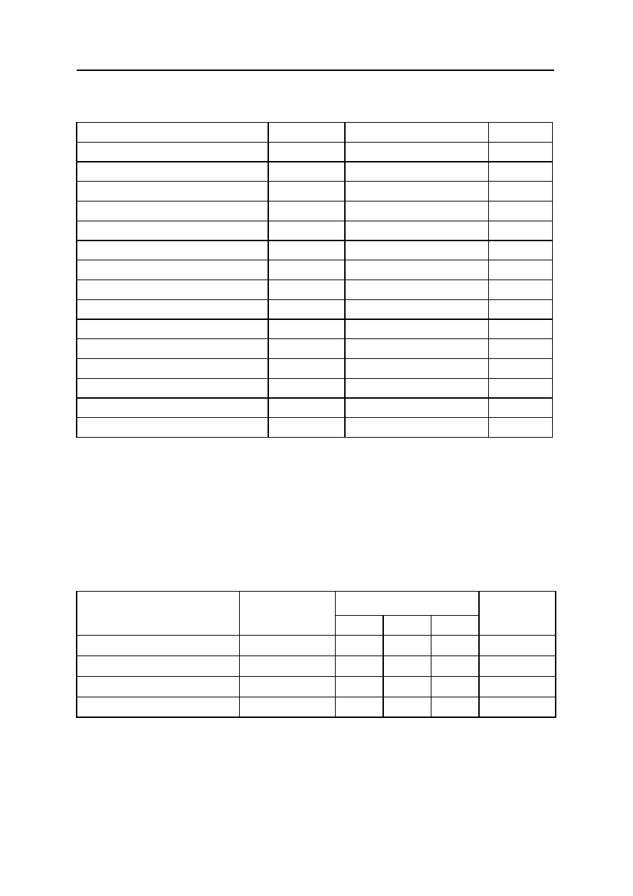
Absolute Maximum Ratings
Ta=25
�C
, unless specified.
Parameter Symbol
Value
Units
Supply Voltage (VSS)
VDD - VSS
-0.5 to +4.0
V
Supply Voltage (VSSM)
VDD - VSSM
-0.5 to +4.0
V
Supply Voltage (VSSB)
VDD - VSSB
-0.5 to +6.0
V
Supply Current*1
ISS
180
mA
Supply Current (VSSM)
ISSM
150
mA
Supply Current (VSSB)
ISSB
150
mA
Output Current (OUT, OUTB, BIAS)
IOUT
150
mA
Input Voltage (DIN, DINB)
VIN
VDD - 2.5 to VDD
V
Input Voltage (DIS)
VINC1
VSS � 0.5 to VDD
+ 0.5
V
Input Voltage (VM)
VINC2
VSS to VSS + 1.5
V
Input Voltage (VB)
VINC3
VSS to VSS + 2.0
V
Output Voltage (OUT, OUTB)
VOUT
VDD � 1.5 to VDD + 1.5
V
Output Voltage (BIAS)
VBIAS
VSSB to VSSB + 3.5V
V
Output Voltage (MODSEN)
VOUTM
VSS to VDD
V
Storage Temperature
Tstg
-55 to + 125
�C
NOTE: *1. Excluding the input current, the modulation current and the bias current.
Recommended Operating Conditions
Value
Parameter Symbol
MIN. TYP. MAX.
Unit
Supply Voltage
VDD - VSS
3.1
3.3
3.5
V
Output Voltage
VOUT -VDD
-1.0
0
1.0
V
BIAS Output Voltage
VBIAS - VSSB
1.3
1.5
3.0
V
Ambient Operating Temperature
Ta
0 25 70
�C

F0539951Q
10.0 Gb/s Laser Diode Driver
Electrical Characteristics
Ta=25�C, V
DD
- V
SS
= V
DD
- V
SSM
= V
DD
- V
SSB
= 3.3V, unless specified
Value
Parameters Symbol
Test
Conditions
MIN. TYP. MAX
Units
Circuit Current *1
ISS
VM - VSS=0[V]
VB - VSS=0[V]
- 95 - mA
Input Voltage
(AC coupled interface)
VIN
Differential
Input
0.4 0.8 1.6 Vp-p
Input Resistor
RIN
Differential
-
100
-
IMmax
25
load
- 65 -
mAp-p
IMmin 25 load, VM
=VSS - 10 -
mAp-p
Modulation Peak Current
IMdis
VDIS=VDD - 0.2V
-
2
-
mA
Output
Resistor
RMOD
- 50 -
IBmax
VBIAS-VSSB =1.3V
100
-
-
mA
Bias Current
IBmin VBIAS-VSSB
=1.3V
VB
=VSS
- 3 - mA
VDISih
Disable operation
VDD
- 0.2
-
VDD
V
Input Voltage
of DIS pin
VDISil
Enable operation
VSS
OPEN VSS+0.2
V
Modulation Monitor Resistor
RMM
-
3
-
Rise Time
Tr
RL = 25, 20% - 80%
- 35 - ps
Fall Time
Tf
RL = 25, 20% - 80%
-
35
-
ps
Maximum Data Rate
fopr
10.0 - - Gb/s
NOTE: *1. Excluding the input current, the modulation current and the bias current.

F0539951Q
10.0 Gb/s Laser Diode Driver
Block Diagram
PAD Descriptions
Symbol Description
VDD Supply
Voltage
VSS,
VSSM, VSSB
Supply Voltage. VSS, VSSM and VSSB are not connected internally.
DIN
Positive data input
DINB
Negative data input
MOD
Positive modulation output (LD should be connected to this pin.)
MODB
Negatibe modulation output
BIAS
Bias current output
VM
Voltage input that sets the LD modulation peak current
VB
Voltage input that sets the bias current
DIS
Voltage input that controls turning on/off modulation current
PWP, PWN
Pulse Width Control
MODSEN
Modulation current monitor output
DIN
DINB
Input
Buffer
PWP
RMODB
MOD
MODB
VSSM
MODSEN
Mod
Buffer
VM
VSSB VB
BIAS
VSS
VDD
3
RMOD
Pulse
Width
Control
PWN
Disable
Control
DIS
Bias
Buffer
DIN
DINB
Input
Buffer
PWP
RMODB
MOD
MODB
VSSM
MODSEN
Mod
Buffer
VM
VSSB VB
BIAS
VSS
VDD
3
RMOD
Pulse
Width
Control
PWN
Disable
Control
DIS
Bias
Buffer

F0539951Q
10.0 Gb/s Laser Diode Driver
Function Table
INPUT OUTPUT
DIN
Current at MOD
Current at MODB
H ON
OFF
L OFF
ON