 | –≠–ª–µ–∫—Ç—Ä–æ–Ω–Ω—ã–π –∫–æ–º–ø–æ–Ω–µ–Ω—Ç: FLK017XP | –°–∫–∞—á–∞—Ç—å:  PDF PDF  ZIP ZIP |

1
Edition 1.3
July 1999
FLK017XP
GaAs FET & HEMT Chips
Item
Saturated Drain Current
Transconductance
Pinch-off Voltage
Gate Source Breakdown Voltage
Power-added Efficiency
Noise Figure
Output Power at 1dB G.C.P.
Power Gain at 1dB G.C.P.
Symbol
IDSS
-
60
90
-
30
-
-1.0
-2.0
-3.5
-5
-
-
7.0
8.0
-
-
26
-
19.5
20.5
-
VDS = 5V, IDS = 3mA
VDS = 5V, IDS = 40mA
VDS = 5V, VGS = 0V
IGS = -3µA
VDS = 10V
IDS 0.6 IDSS
f = 14.5GHz
VDS = 3V
IDS = 20mA
f = 12GHz
VDS = 10V
IDS = 36mA
f = 12GHz
mA
mS
V
dB
%
-
2.5
-
dB
dBm
V
gm
Vp
VGSO
P1dB
G1dB
add
NF
Associated Gain
-
7
-
dB
Gas
Maximum Availble Gain
-
11
-
dB
Ga(max)
Test Conditions
Unit
Limit
Typ.
Max.
Min.
ELECTRICAL CHARACTERISTICS (Ambient Temperature Ta=25∞C)
Note: RF parameter sample size 10pcs. criteria (accept/reject)=(2/3)
G.C.P.: Gain Compression Point
Channel to Case
-
65
130
∞C/W
Thermal Resistance
Rth
The chip must be enclosed in a hermetically sealed environment for optimum performance and reliability.
DESCRIPTION
The FLK017XP chip is a power GaAs FET that is designed for
general purpose applications in the Ku-Band frequency range as it
provides superior power, gain, and efficiency.
Fujitsu's stringent Quality Assurance Program assures the highest
reliability and consistent performance.
Item
Drain-Source Voltage
Gate-Source Voltage
Total Power Dissipation
Storage Temperature
Channel Temperature
Symbol
VDS
VGS
15
-5
1.15
-65 to +175
175
Tc = 25∞C
V
V
W
∞C
∞C
Ptot
Tstg
Tch
Condition
Unit
Rating
ABSOLUTE MAXIMUM RATING (Ambient Temperature Ta=25∞C)
Fujitsu recommends the following conditions for the reliable operation of GaAs FETs:
1. The drain-source operating voltage (VDS) should not exceed 10 volts.
2. The forward and reverse gate currents should not exceed 1.34 and -0.05 mA respectively with
gate resistance of 3000.
3. The operating channel temperature (Tch) should not exceed 145∞C.
FEATURES
∑ High Output Power: P1dB = 20.5dBm(Typ.)
∑ High Gain: G1dB = 8.0dB(Typ.)
∑ High PAE: add = 26%(Typ.)
∑ Proven Reliability
Drain
Source
Source
Gate

2
FLK017XP
GaAs FET & HEMT Chips
POWER DERATING CURVE
DRAIN CURRENT vs. DRAIN-SOURCE VOLTAGE
1
2
0
50
100
150
200
2
4
6
8
10
Case Temperature (∞C)
Drain-Source Voltage (V)
Total Power Dissipation (W)
20
18
16
14
12
2
4
6
8
10
12
14
Input Power (dBm)
Output Power (dBm)
60
40
20
Drain Current (mA)
VGS =0V
-0.5V
-1.5V
-2.0V
-1.0V
OUTPUT POWER vs. INPUT POWER
VDS=10V
IDS0.6IDSS
f = 14.5GHz
add
Pout
40
20
add
(%)
21
22
20
19
18
8
9
10
Drain-Source Voltage (V)
P
1dB
(dBm)
P1dB & add vs. VDS
f = 14.5GHz
IDS0.6IDSS
add
P1dB
30
40
20
add
(%)
3
FLK017XP
GaAs FET & HEMT Chips
S-PARAMETERS
VDS = 10V, IDS = 40mA
FREQUENCY
S11
S21
S12
S22
(MHZ)
MAG
ANG
MAG
ANG
MAG
ANG
MAG
ANG
100
1.000
-1.9
2.832
178.4
.001
88.9
.846
-0.6
500
.998
-9.5
2.824
171.9
.007
84.7
.845
-2.9
1000
.992
-18.9
2.799
163.9
.014
79.5
.842
-5.7
1500
.982
-28.2
2.758
156.0
.021
74.3
.838
-8.5
2000
.969
-37.4
2.703
148.3
.028
69.4
.832
-11.2
2500
.953
-46.3
2.638
140.7
.034
64.6
.825
-13.8
3000
.936
-55.0
2.564
133.4
.039
60.0
.817
-16.4
3500
.918
-63.5
2.485
126.2
.044
55.6
.809
-18.8
4000
.899
-71.6
2.401
119.4
.049
51.5
.800
-21.2
4500
.881
-79.5
2.316
112.7
.053
47.6
.792
-23.5
5000
.863
-87.1
2.231
106.3
.056
44.0
.784
-25.8
5500
.846
-94.4
2.147
100.1
.059
40.6
.776
-28.0
6000
.830
-101.5
2.064
94.1
.062
37.3
.769
-30.1
6500
.816
-108.3
1.985
88.3
.064
34.3
.762
-32.2
7000
.802
-114.8
1.908
82.7
.066
31.5
.755
-34.3
7500
.791
-121.1
1.834
77.2
.067
28.9
.749
-36.4
8000
.780
-127.1
1.764
72.0
.069
26.4
.744
-38.4
8500
.771
-133.0
1.697
66.8
.070
24.1
.739
-40.5
9000
.764
-138.6
1.634
61.8
.071
21.9
.735
-42.5
9500
.757
-143.9
1.574
57.0
.072
19.8
.731
-44.6
10000
.752
-149.1
1.516
52.2
.072
17.9
.727
-46.7
10500
.747
-154.1
1.462
47.6
.073
16.1
.724
-48.8
11000
.744
-158.9
1.410
43.0
.073
14.4
.721
-51.0
11500
.741
-163.5
1.361
38.6
.073
12.8
.718
-53.2
12000
.739
-168.0
1.314
34.2
.073
11.3
.716
-55.4
12500
.738
-172.3
1.269
29.9
.073
9.9
.713
-57.6
13000
.738
-176.4
1.227
25.7
.073
8.6
.711
-59.8
13500
.738
179.6
1.186
21.6
.073
7.3
.710
-62.1
14000
.739
175.8
1.147
17.5
.073
6.2
.708
-64.5
14500
.740
172.1
1.110
13.5
.073
5.1
.707
-66.8
15000
.742
168.5
1.074
9.5
.072
4.1
.706
-69.2
15500
.744
165.1
1.039
5.6
.072
3.1
.705
-71.7
16000
.746
161.8
1.006
1.7
.072
2.3
.704
-74.2
16500
.749
158.5
.974
-2.1
.071
1.5
.704
-76.7
17000
.752
155.5
.943
-5.9
.071
0.7
.703
-79.2
17500
.755
152.5
.913
-9.6
.071
0.0
.703
-81.8
18000
.758
149.6
.885
-13.3
.070
-0.6
.703
-84.5
18500
.761
146.8
.856
-16.9
.070
-1.2
.703
-87.1
19000
.765
144.1
.829
-20.5
.070
-1.7
.703
-89.8
19500
.768
141.4
.803
-24.1
.070
-2.2
.704
-92.6
20000
.772
138.9
.777
-27.7
.069
-2.7
.704
-95.3
NOTE:*
The data includes bonding wires.
n: number of wires
Gate
n=1 (0.2mm length, 25µm Dia Au wire)
Drain n=1 (0.2mm length, 25µm Dia Au wire)
Source n=4 (0.3mm length, 25µm Dia Au wire)
Download S-Parameters, click here
For further information please contact:
FUJITSU COMPOUND SEMICONDUCTOR, INC.
2355 Zanker Rd.
San Jose, CA 95131-1138, U.S.A.
Phone: (408) 232-9500
FAX: (408) 428-9111
www.fcsi.fujitsu.com
FUJITSU MICROELECTRONICS, LTD.
Compound Semiconductor Division
Network House
Norreys Drive
Maidenhead, Berkshire SL6 4FJ
Phone:+44 (0)1628 504800
FAX:+44 (0)1628 504888
Fujitsu Limited reserves the right to change products and specifications without notice.
The information does not convey any license under rights of Fujitsu Limited or others.
© 1998 FUJITSU COMPOUND SEMICONDUCTOR, INC.
Printed in U.S.A. FCSI0598M200
Fujitsu Compound Semiconductor Products contain gallium arsenide
(GaAs) which can be hazardous to the human body and the environment.
For safety, observe the following procedures:
CAUTION
∑ Do not put these products into the mouth.
∑ Do not alter the form of this product into a gas, powder, or liquid
through burning, crushing, or chemical processing as these by-products
are dangerous to the human body if inhaled, ingested, or swallowed.
∑ Observe government laws and company regulations when discarding this
product. This product must be discarded in accordance with methods
specified by applicable hazardous waste procedures.
4
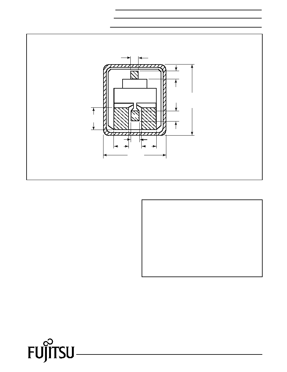
CHIP OUTLINE
Source electrodes are electrically
insulated from the bottom of the
chip (PHS)
Die Thickness: 60±20µm
40
40
70
50
Drain
Source
Source
Gate
60
110
410
±
30
70
330±30
(Unit: µm)
FLK017XP
GaAs FET & HEMT Chips