1
Edition 1.2
July 1999
FLU10XM
L-Band Medium & High Power GaAs FET
Item
Drain-Source Voltage
V
Gate-Source Voltage
V
Total Power Dissipation
Storage Temperature
Channel Temperature
W
∞C
∞C
Symbol
VDS
VGS
PT
Tstg
Tch
15
-5
4.16
-65 to +175
+175
Rating
Tc = 25∞C
Condition
Unit
ABSOLUTE MAXIMUM RATINGS (Ambient Temperature Ta=25∞C)
Fujitsu recommends the following conditions for the reliable operation of GaAs FETs:
1. The drain-source operating voltage (VDS) should not exceed 10 volts.
2. The forward and reverse gate currents should not exceed 4.8 and -0.5 mA respectively with
gate resistence of 400.
3. The operating channel temperature (Tch) should not exceed 145∞C.
Item
Drain Current
Transconductance
Pinch-Off Voltage
Gate-Source Breakdown Voltage
Output Power at 1 dB G.C.P.
Power Gain at 1 dB G.C.P.
Power Added Efficiency
Thermal Resistance
Symbol
I
DSS
V
GSO
-
150
-
-
300
450
-1.0
-2.0
-3.5
-5
-
-
28.5
29.5
-
13.5
14.5
-
-
47
-
-
25
36
V
DS
= 5V, V
GS
=0V
V
DS
= 5V, I
DS
=200mA
V
DS
= 5V, I
DS
=15mA
I
GS
= -15µA
Channel to Case
G.C.P.: Gain Compression Point
Case Style: XM
V
DS
= 10V
f=2.0 GHz
I
DS
=0.6I
DSS
mA
mS
V
dB
dBm
V
∞C/W
%
gm
V
p
P
1dB
G
1dB
add
R
th
Conditions
Unit
Limits
Typ.
Max.
Min.
ELECTRICAL CHARACTERISTICS (Ambient Temperature Ta=25∞C)
Note: The RF parameters are measured on a lot basis by sample testing
at an AQL = 0.1%, Level-II inspection. Any lot failure shall be 100% retested.
FEATURES
∑ High Output Power: P1dB=29.5dBm (Typ.)
∑ High Gain: G1dB=14.5dB (Typ.)
∑ High PAE: add=47% (Typ.)
∑ Hermetic Metal/Ceramic (SMT) Package
∑ Tape and Reel Available
DESCRIPTION
The FLU10XM is a GaAs FET designed for base station applications in the
PCN/PCS frequency range. This is a new product series that uses a surface
mount package that has been optimized for high volume cost driven applications.
Fujitsu's stringent Quality Assurance Program assures the highest
reliability and consistent performance.
2
FLU10XM
L-Band Medium & High Power GaAs FET
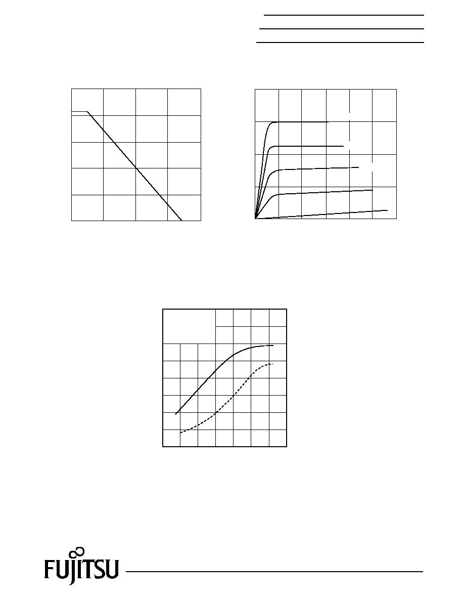
POWER DERATING CURVE
DRAIN CURRENT vs. DRAIN-SOURCE VOLTAGE
2
1
4
5
3
0
50
100
150
200
2
0
4
6
8
10
Case Temperature (∞C)
Drain-Source Voltage (V)
Total Power Dissipation (W)
100
300
200
Drain Current (mA)
VGS =0V
-0.5V
-1.5V
-2.0V
-1.0V
OUTPUT POWER vs. INPUT POWER
VDS=10V
IDS 0.6IDSS
f = 2.0 GHz
8
10
12
14
16
18
Input Power (dBm)
30
28
26
24
22
20
30
40
50
20
10
Output Power (dBm)
add
Pout
add
(%)
4
For further information please contact:
FUJITSU COMPOUND SEMICONDUCTOR, INC.
2355 Zanker Rd.
San Jose, CA 95131-1138, U.S.A.
Phone: (408) 232-9500
FAX: (408) 428-9111
www.fcsi.fujitsu.com
FUJITSU MICROELECTRONICS, LTD.
Compound Semiconductor Division
Network House
Norreys Drive
Maidenhead, Berkshire SL6 4FJ
Phone:+44 (0)1628 504800
FAX:+44 (0)1628 504888
Fujitsu Limited reserves the right to change products and specifications without notice.
The information does not convey any license under rights of Fujitsu Limited or others.
© 1998 FUJITSU COMPOUND SEMICONDUCTOR, INC.
Printed in U.S.A. FCSI0598M200
Fujitsu Compound Semiconductor Products contain gallium arsenide
(GaAs) which can be hazardous to the human body and the environment.
For safety, observe the following procedures:
CAUTION
∑ Do not put these products into the mouth.
∑ Do not alter the form of this product into a gas, powder, or liquid
through burning, crushing, or chemical processing as these by-products
are dangerous to the human body if inhaled, ingested, or swallowed.
∑ Observe government laws and company regulations when discarding this
product. This product must be discarded in accordance with methods
specified by applicable hazardous waste procedures.
FLU10XM
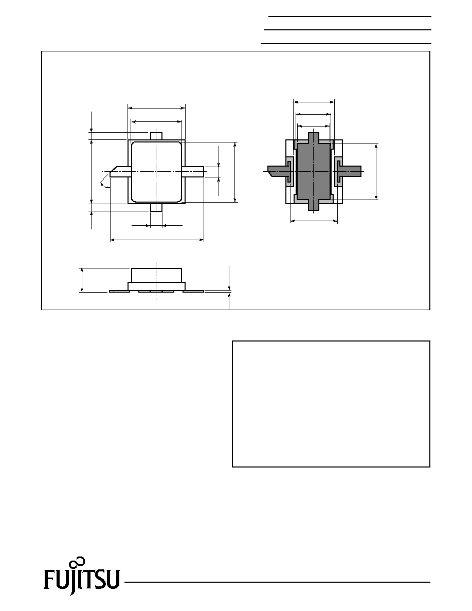
L-Band Medium & High Power GaAs FET
3.8±0.15
(0.150)
3.35
(0.132)
4.4
±
0.15
(0.173)
4.2
±
0.1
(0.165)
0.7
(0.028)
0.5
(0.020)
0.5
(0.020)
1.7
±
0.2
(0.067)
0.15
±
0.05
(0.006)
Unit: mm(inches)
1. Gate
2. Source
3. Drain
2.865
(0.112)
3.13±0.15
2.265
(0.089)
2.0±0.15
4.0
±
0.15
(0.159)
Case Style "XM"
Metal-Ceramic Hermetic Package
2
45
∞
1
3
0.7
(0.028)
6.3
(0.248)