 | –≠–ª–µ–∫—Ç—Ä–æ–Ω–Ω—ã–π –∫–æ–º–ø–æ–Ω–µ–Ω—Ç: P0120004P | –°–∫–∞—á–∞—Ç—å:  PDF PDF  ZIP ZIP |

Technical Note
P0120004P
1.5W GaAs Power FET (Pb-Free Type)
SUMITOMO ELECTRIC
Specifications and information are subject to change without notice. 2003-11
Sumitomo Electric Industries, Ltd. 1,Taya-cho, Sakae-ku, Yokohama, 244-8588 Japan
Phone: +81-45-853-7263 Fax: +81-45-853-1291 e-mail :
GaAsIC-ml@ml.sei.co.jp
Features
4
1
2
3
4
1
2
3
∑ Up to 2.7 GHz frequency band
Web Site:
www.sei.co.jp/GaAsIC/
∑ Beyond +30 dBm output power
∑ Up to +45dBm Output IP3
∑ High Drain Efficiency
∑ 11dB Gain at 2.1GHz
∑ SOT-89 SMT Package
∑ Low Noise Figure
Applications
∑Wireless communication system
∑Cellular, PCS, PHS, W-CDMA, WLAN
Description
P0120004P is a high performance GaAs MESFET housed in
a low-cost SOT-89 package. Our originally developed
"pulse-doped" channel structure has realized low distortion,
which leads to high IP3. The channel structure also achieved
an extremely low noise figure. The details about pulse-doped
FET channel are described in our products catalog.
Utilization of AuSn die attach has realized a low and stable
thermal resistance. The lead frame is plated with Sn-Bi to
make the device Pb-free.
SEI's long history of manufacturing has cultivated high
device reliability. The estimated MTTF of the FET is longer
than 15years at Tj of 150∞C. You can see the details in
Reliability and Quality Assurance.
Functional Diagram
Pin No.
Function
1 Input/Gate
2, 4
Ground
3 Output/Drain
Ordering Information
Part No
Description
Number
of devices
Container
P0120004P
GaAs Power FET
1000
7" Reel
KP024J
2.11-2.17GHz
Application Circuit
1
Anti-static
Bag
Absolute Maximum Ratings
(@Tc=25∞C)
Parameter
Symbol Value Units
Drain-Source Voltage
Vds
8
V
Gate-Source Voltage
Vgs
- 4
V
Drain Current
Ids
Idss
---
RF Input Power
(continuous)
Pin 25
(*)
dBm
Power Dissipation
Pt 4.3 W
Junction Temperature
Tj
125
∞C
Storage Temperature
Tstg
- 40 to +125
∞C
Tc: Case Temperature. Operating the device beyond any of these
values may cause permanent damage.
(*) Measured at 2.1GHz with our test fixture matched to IP3.
Electrical Specifications (@Tc=25∞C)
Values
Parameter Symbol
Test
Conditions
Min. Typ. Max.
Units
Saturated Drain Current
Idss
Vds=3V, Vg=0V
---
---
1600
mA
Transconductance gm
Vds=6V, Ids=500mA
450
---
---
mS
Pinchoff Voltage
Vp
Vds=6V, Ids=50mA
- 3.0
---
- 1.7
V
Gate-Source Breakdown Voltage
|Vgs0|
Igso= - 50
µA
3.0 --- --- V
DC
Thermal Resistance
Rth
Channel-Case
---
--- 22
∞C/W
Frequency f
2.7
GHz
Output Power
@ 1dB Gain Compression
P1dB
32
---
dBm
Small Signal Gain
G
11
---
dB
Output IP3
IP3
---
45
---
dBm
RF
Power Added Efficiency
add
Vds=6V
Ids=400mA
f=2.1GHz
---
60 --- %
-1-

Technical Note
P0120004P
1.5W GaAs Power FET (Pb-Free Type)
SUMITOMO ELECTRIC
Typical Characteristics
Vgs=0V
-2.0V
-1.5V
-1.0V
-0.5V
D
r
a
i
n C
u
rre
n
t
(m
A
)
Vds (V)
2000
1500
1000
500
0
0
2
4
6
T
o
ta
l P
o
w
e
r
D
i
s
s
i
p
a
ti
o
n
(
W
)
0
2
4
6
T
o
ta
l P
o
w
e
r
D
i
s
s
i
p
a
ti
o
n
(
W
) 6
5
4
3
2
1
0 0
50
100
150
200
Transfer Curve
Power Derating Curve
Tc (∞C)
8
8
Load-pull Characteristics (Typical Data)
Tc=25∞C, Vds=6V, Ids=400mA, Common Source, Zo=50
(Calibrated to device leads)
0
45
90
13
5
-180
-135
-9
0
-45
0
45
90
13
5
-180
-135
-9
0
-45
S12
S21
1.2GHz
1.2GHz
2.4GHz
2.4GHz
2.0
6.0
4.0
0
0.02
0.04
0.06
0
Scale for |S12|
S
c
a
l
e
fo
r |
S
2
1
|
0
1.
0
1.
0
-1
.
0
10
.
0
10.0
-10
.0
5.
0
5.0
-5.
0
2.
0
2.
0
-2
.0
3.
0
3.0
-3.
0
4.
0
4.0
-4.
0
0.
2
0.2
-0.2
0.
4
0.4
-0.
4
0.
6
0.
6
-0
.6
0.
8
0.
8
-0
.8
0
1.
0
1.
0
-1
.
0
10
.
0
10.0
-10
.0
5.
0
5.0
-5.
0
2.
0
2.
0
-2
.0
3.
0
3.0
-3.
0
4.
0
4.0
-4.
0
0.
2
0.2
-0.2
0.
4
0.4
-0.
4
0.
6
0.
6
-0
.6
0.
8
0.
8
-0
.8
S11
S22
1.2GHz
1.2GHz
2.4GHz
2.4GHz
Specifications and information are subject to change without notice. 2003-11
Sumitomo Electric Industries, Ltd. 1,Taya-cho, Sakae-ku, Yokohama, 244-8588 Japan
Phone: +81-45-853-7263 Fax: +81-45-853-1291 e-mail :
GaAsIC-ml@ml.sei.co.jp
-2-
Web Site:
www.sei.co.jp/GaAsIC/
Technical Note
P0120004P
1.5W GaAs Power FET (Pb-Free Type)
SUMITOMO ELECTRIC
Tc=25∞C, Vds=6V, Ids=350mA, Common Source, Zo=50
(Calibrated to device leads)
0
45
90
13
5
-180
-135
-9
0
-45
0
45
90
13
5
-180
-135
-9
0
-45
S12
S21
1.2GHz
1.2GHz
2.4GHz
2.4GHz
2.0
6.0
4.0
0
0.02
0.04
0.06
0
Scale for |S12|
S
c
al
e f
o
r
|
S
2
1
|
0
1.
0
1.
0
-1
.0
10
.
0
10.0
-10
.0
5.
0
5.0
-5.
0
2.0
2.
0
-2
.0
3.
0
3.0
-3.
0
4.0
4.0
-4.
0
0.2
0.2
-0.2
0.4
0.4
-0
.4
0.
6
0.
6
-0
.6
0.
8
0.
8
-0
.8
0
1.
0
1.
0
-1
.0
10
.
0
10.0
-10
.0
5.
0
5.0
-5.
0
2.0
2.
0
-2
.0
3.
0
3.0
-3.
0
4.0
4.0
-4.
0
0.2
0.2
-0.2
0.4
0.4
-0
.4
0.
6
0.
6
-0
.6
0.
8
0.
8
-0
.8
S11
S22
1.2GHz
1.2GHz
2.4GHz
2.4GHz
Ids
Ids
=400mA Freq (GHz) S11 Mag
S11 Ang
S21 Mag
S21 Ang
S12 Mag
S12 Ang
S22 Mag
S22 Ang
1.2
0.841
173.7
4.002
66.2
0.040
34.2
0.459
167.3
1.4
0.843
165.7
3.433
58.9
0.043
32.8
0.464
162.8
1.6
0.845
158.6
3.005
52.1
0.046
31.0
0.470
158.6
1.8
0.847
152.2
2.673
45.5
0.049
28.9
0.475
154.2
2.0
0.848
146.1
2.410
39.1
0.052
26.4
0.481
149.6
2.2
0.849
140.2
2.200
32.7
0.056
23.6
0.488
145.1
2.4
0.849
134.1
2.028
26.3
0.059
20.2
0.499
140.1
=350mA Freq (GHz) S11 Mag
S11 Ang
S21 Mag
S21 Ang
S12 Mag
S12 Ang
S22 Mag
S22 Ang
1.2
0.841
173.6
3.993
66.2
0.040
33.4
0.465
167.2
1.4
0.843
165.6
3.424
59.0
0.044
31.9
0.471
162.7
1.6
0.845
158.6
2.998
52.2
0.047
30.2
0.476
158.4
1.8
0.846
152.2
2.666
45.6
0.050
28.1
0.482
154.0
2.0
0.847
146.1
2.405
39.2
0.053
25.5
0.488
149.4
2.2
0.848
140.2
2.195
32.8
0.056
22.8
0.494
144.8
2.4
0.848
134.1
2.024
26.4
0.060
19.5
0.505
139.8
[Note]
You can download the S-parameter list from our web site:
www.sei.co.jp/GaAsIC
/
Specifications and information are subject to change without notice. 2003-11
Sumitomo Electric Industries, Ltd. 1,Taya-cho, Sakae-ku, Yokohama, 244-8588 Japan
Phone: +81-45-853-7263 Fax: +81-45-853-1291 e-mail :
GaAsIC-ml@ml.sei.co.jp
-3-
Web Site:
www.sei.co.jp/GaAsIC/

Technical Note
P0120004P
1.5W GaAs Power FET (Pb-Free Type)
SUMITOMO ELECTRIC
Ids=350mA
Ids=400mA
-100
-80
-60
-40
-20
0
20
40
60
80
-15
-10
-5
0
5
10
15
20
25
Po
u
t
(
d
B
m
)
Ga
i
n
(
d
B
)
IM
3
(
d
B
m
)
IP
3
(
d
B
m
)
IM
3
/
P
o
u
t
(
d
B
c
)
ad
d
(
%
)
Pin (dBm)
Pout
Gain
IP3
add
IM3
IM3/Pout
-100
-80
-60
-40
-20
0
20
40
60
80
-15
-10
-5
0
5
10
15
20
25
Po
u
t
(
d
B
m
)
G
a
in (
d
B
)
IM
3
(
d
B
m
)
IP
3
(
d
B
m
)
IM
3
/
P
o
u
t
(
d
B
c
)
ad
d
(
%
)
Pin (dBm)
Pout
Gain
IP3
add
IM3
IM3/Pout
-100
-80
-60
-40
-20
0
20
40
60
80
-15
-10
-5
0
5
10
15
20
25
Po
u
t
(
d
B
m
)
G
a
in (
d
B
)
IM
3
(
d
B
m
)
IP
3
(
d
B
m
)
IM
3
/
P
o
u
t
(
d
B
c
)
ad
d
(
%
)
Pin (dBm)
Pout
Gain
IP3
add
IM3
IM3/Pout
-100
-80
-60
-40
-20
0
20
40
60
80
-15
-10
-5
0
5
10
15
20
25
Po
u
t
(
d
B
m
)
G
a
in (
d
B
)
IM
3
(
d
B
m
)
IP
3
(
d
B
m
)
IM
3
/
P
o
u
t
(
d
B
c
)
ad
d
(
%
)
Pin (dBm)
Pout
Gain
IP3
add
IM3
IM3/Pout
Device: P0120004P
Frequency: f1=2.1GHz, f2=2.101GHz
Bias: Vds=6V, Ids=400mA
Source Matching: Mag 0.65 Ang -156.0∞
Load Matching: Mag 0.67 Ang -140.8∞
Device: P0120004P
Frequency: f1=2.1GHz, f2=2.101GHz
Bias:Vds=6V, Ids=350mA
Source Matching: Mag 0.65 Ang -156.0∞
Load Matching: Mag 0.635 Ang -142.2∞
[Note] P
out
and
add
are measured by one signal.
The data for the figures above were measured with the load impedance matched to IP3.
Id=400mA
Pin
(dBm)
Pout
(dBm)
Gain
(dB)
IM3
(dBm)
IM3/Pout
(dBc)
IP3
(dBm)
Id
(mA)
add
(%)
-10.0
1.5
11.5
-73.3
-74.8
38.9
406.0
0.1
-5.0
6.6
11.6
-67.2
-73.8
43.6
402.8
0.2
0.0
11.5
11.5
-56.3
-67.8
45.2
396.6
0.6
5.0
16.6
11.6
-40.6
-57.2
45.1
384.9
1.8
10.0
21.7
11.7
-21.6
-43.3
43.2
367.0
6.3
15.0
26.5
11.5
2.2
-24.3
38.0
381.9
18.2
20.0
30.8
10.8
17.3
-13.5
34.7
455.0
40.3
Id=350mA
Pin
(dBm)
Pout
(dBm)
Gain
(dB)
IM3
(dBm)
IM3/Pout
(dBc)
IP3
(dBm)
Id
(mA)
add
(%)
-10.0
2.0
12.0
-72.5
-74.5
39.0
356.6
0.1
-5.0
7.1
12.1
-65.7
-72.8
43.5
353.3
0.2
0.0
12.0
12.0
-53.3
-65.3
44.5
346.9
0.7
5.0
17.0
12.0
-38.5
-55.5
44.7
336.4
2.3
10.0
22.1
12.1
-18.3
-40.3
42.1
319.2
7.9
15.0
26.9
11.9
4.1
-22.8
37.5
339.5
22.4
20.0
31.0
11.0
17.8
-13.2
34.7
412.1
46.8
Specifications and information are subject to change without notice. 2003-11
Sumitomo Electric Industries, Ltd. 1,Taya-cho, Sakae-ku, Yokohama, 244-8588 Japan
Phone: +81-45-853-7263 Fax: +81-45-853-1291 e-mail :
GaAsIC-ml@ml.sei.co.jp
-4-
Web Site:
www.sei.co.jp/GaAsIC/

Specifications and information are subject to change without notice. 2003-11
Sumitomo Electric Industries, Ltd. 1,Taya-cho, Sakae-ku, Yokohama, 244-8588 Japan
Phone: +81-45-853-7263 Fax: +81-45-853-1291 e-mail :
GaAsIC-ml@ml.sei.co.jp
Web Site:
www.sei.co.jp/GaAsIC/
-5-
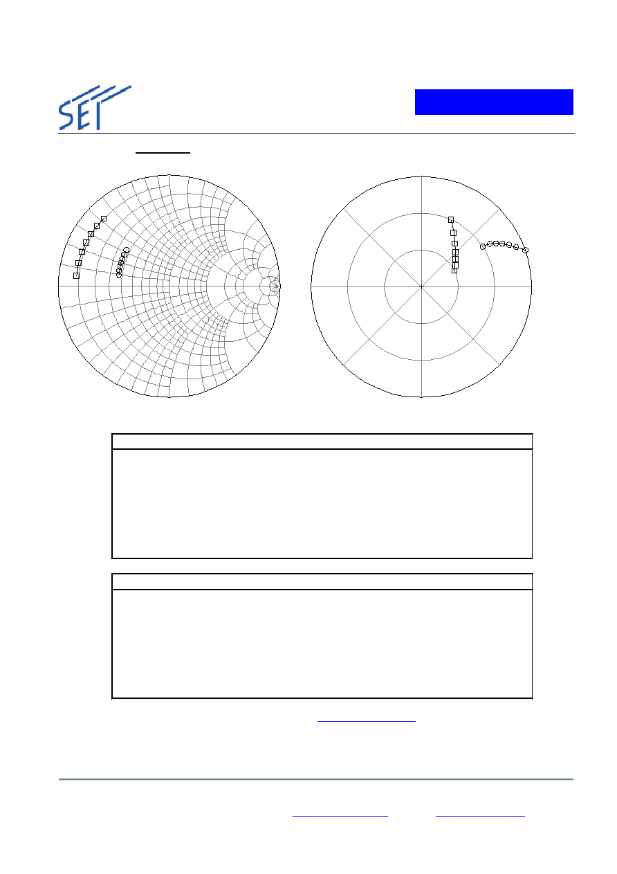
Technical Note
P0120004P
1.5W GaAs Power FET (Pb-Free Type)
SUMITOMO ELECTRIC
Tc=25∞C, Vds=6V, Ids=400mA, Pin=5d Bm
[Pout-Lstate]
f = 2.1GHz
pout
: 0.48
172.8
Source : 0.81
-152.1
Pout max : 17.5d Bm
[IP3-Lstate]
f1 = 2.1GHz
f2 = 2.101GHz
IP3
: 0.69
-141.8
Source : 0.77
-155.2
IP3 max : 45.6d Bm
Tc=25∞C, Vds=6V, Ids=350mA, Pin=5d Bm
[Pout-Lstate]
f = 2.1GHz
pout
: 0.50
177.2
Source : 0.81
-152.1
Pout max : 17.95dBm
[IP3-Lstate]
f1 = 2.1GHz
f2 = 2.101GHz
IP3
: 0.66
-142.0
Source : 0.77
-155.2
IP3 max : 43.9d Bm
+j50
16.25
17.5
+j25
+j100
-j100
-j50
-j25
25
50
100
16.25
17.5
+j25
+j100
-j100
-j50
-j25
25
50
100
43.1
+j25
+j50
+j100
-j100
-j50
-j25
25
50
100
45.6
43.1
+j25
+j50
+j100
-j100
-j50
-j25
25
50
100
45.6
16.7
+j25
+j50
+j100
-j100
-j50
-j25
25
50
100
17.95
16.7
+j25
+j50
+j100
-j100
-j50
-j25
25
50
100
17.95
41.4
+j25
+j50
+j100
-j100
-j50
-j25
25
50
100
43.9
41.4
+j25
+j50
+j100
-j100
-j50
-j25
25
50
100
43.9