 | –≠–ª–µ–∫—Ç—Ä–æ–Ω–Ω—ã–π –∫–æ–º–ø–æ–Ω–µ–Ω—Ç: P02221B2P | –°–∫–∞—á–∞—Ç—å:  PDF PDF  ZIP ZIP |
T
Specifications and information are subject to change without notice. 2005-07
Eudyna Devices Inc. 1,Kanai-cho, Sakae-ku, Yokohama, 244-0845 Japan
echnical Note
P02221B2P
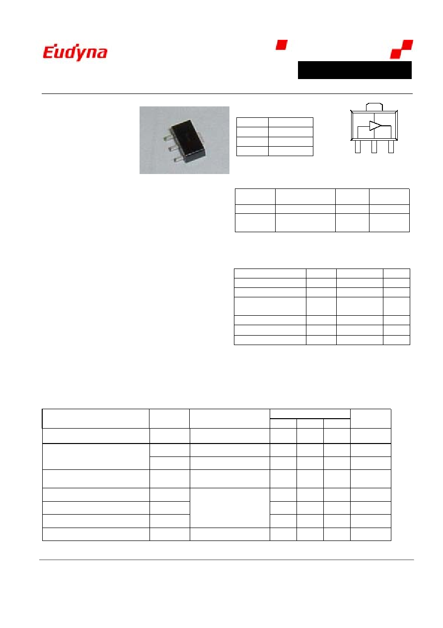
500mW InGaP HBT Amplifier
Features
∑1.8 to 2.5GHz Frequency Band
∑+26.5dBm Output Power
∑+43dBm Output IP3
∑+5V Single Supply Voltage
∑14dB Gain at 2.14GHz
∑Highly Reliable InGaP HBT
∑Pb-free SOT-89 SMT Package
∑AuSn Die Attach for Low and
Stable Thermal Resistance
Applications
∑Wireless communication system
∑Cellular, PCS, PHS, W-CDMA, WLAN
Description
P02221B2P is a high performance InGaP/GaAs HBT
amplifier housed in a low-cost SOT-89 package. The
hetero-junction epitaxial structure has been designed to
achieve low distortion, which leads to high IP3. The device
needs only a +5V single power supply voltage in operation.
Utilization of AuSn die attach has realized a low and stable
thermal resistance.
Functional Diagram
Pin No.
Function
1 RF
Input
2, 4
Ground
3 RF
Output
Ordering Information
Part No
Description
Number
of devices
Container
P02221B2P
HBT Amplifier
1000
7" Reel
KP035J
2.14GHz
Application Circuit
1
Anti-static
Bag
Absolute Maximum Ratings
(@Tc=25∞C)
Parameter Symbol
Value
Units
Device Voltage
Vd
6
V
Device Current
Id
500
mA
RF Input Power
(continuous)
Pin 15
dBm
Power Dissipation
Pt
2
W
Junction Temperature
Tj
+150
∞C
Storage Temperature
Tstg
- 40 to +150
∞C
Tc: Case Temperature. Operating the device beyond any of these
values may cause permanent damage.
Electrical Specifications (@Tc=
+
25∞C, Vs=
+
5V) Measured at 2140MHz using application circuit.
Values
Parameter
Symbol Test
Conditions
Min.
Typ. Max.
Units
Consumption Current
Is
RF=off
247
294
341
mA
IP3_12 Pout=12dBm
S.C.L. --- 43 --- dBm
Output IP3
IP3_15 Pout=15dBm
S.C.L. 38.5 41 --- dBm
Output Power
@ 1dB Gain Compression
P1dB ---
24.5
26.5
---
dBm
Small Signal Gain
Ga
12.5
14
---
dB
Input Return Loss
S11
---
-10 --- dB
Output Return Loss
S22
Pin=-10dBm
---
-8 --- dB
Thermal Resistance
Rth
Junction-Case
---
37 --- ∞C/W
4
3
1
2
Phone : +81-45-853-8150 Fax : +81-45-853-8170 e-mail : www-sales-s@eudyna.com Web Site : www.eudyna.com
-1-

Technical Note
P02221B2P
500mW InGaP HBT Amplifier
Specifications and information are subject to change without notice. 2005-07
Eudyna Devices Inc. 1,Kanai-cho, Sakae-ku, Yokohama, 244-0845 Japan
Application Circuit : 2140MHz
Vs
RF in
RF out
R1
R2
R3
C1
C2
C3
L2
L1
C6
C7
C5
C4
L3
3.3
360
360
15nH
16nH
82pF
82pF
0.75pF
2.7nH
50 EL1
2.4pF
18pF
1uF
1000pF
DUT
4.5deg
Vd
-40
-30
-20
-10
0
10
20
1.9
2.0
2.1
2.2
2.3
Frequency (GHz)
S-parameters (dB)
S21
S12
S11
S22
RF in
RF out
R1
R2
R3
C1
C2
C3
C6
C7
C4
L1
L2
L3
Vs
Gnd
C5
Phone : +81-45-853-8150 Fax : +81-45-853-8170 e-mail : www-sales-s@eudyna.com Web Site : www.eudyna.com
-2-
Technical Note
P02221B2P
500mW InGaP HBT Amplifier
Specifications and information are subject to change without notice. 2005-07
Eudyna Devices Inc. 1,Kanai-cho, Sakae-ku, Yokohama, 244-0845 Japan
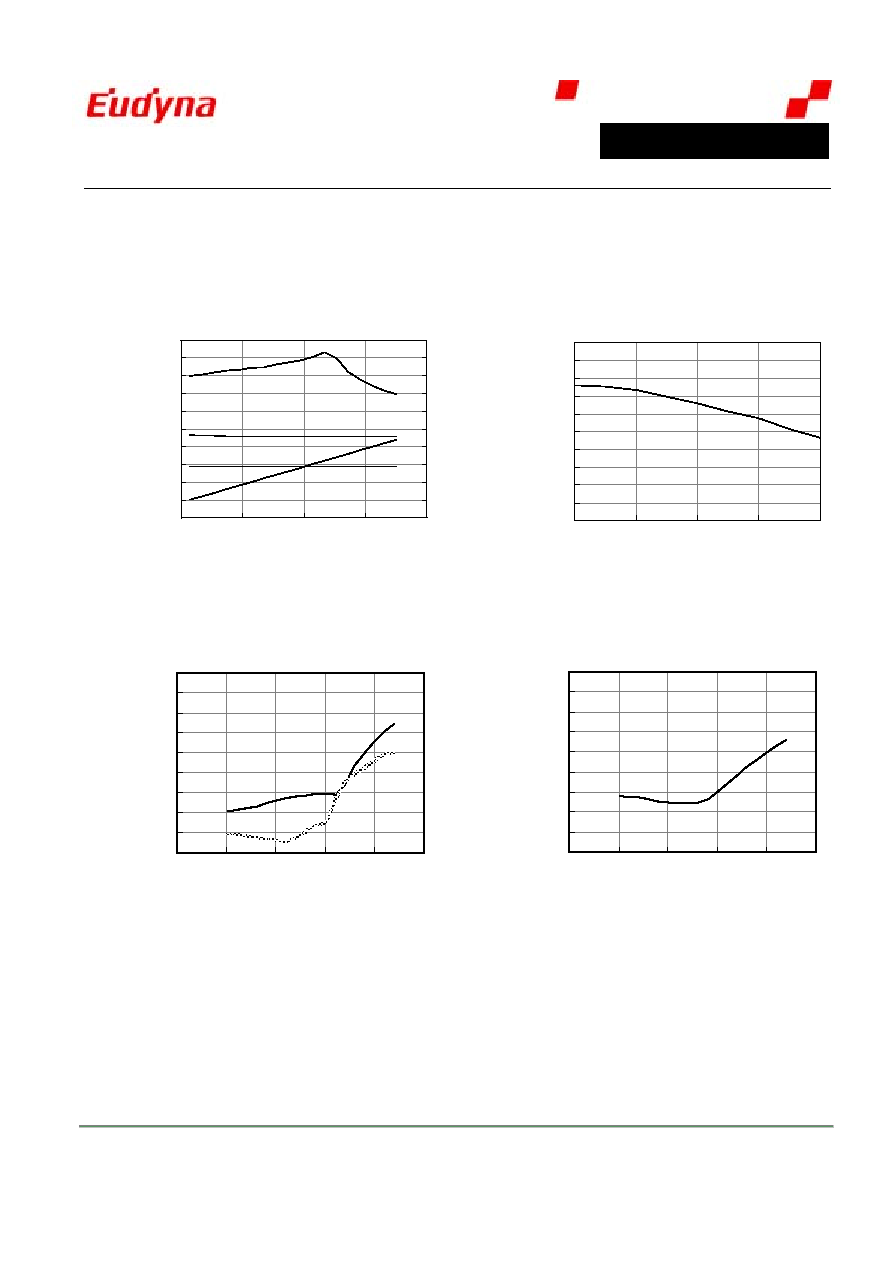
[Typical Performance]
KP035J Application Circuit
(Vs=5V, Tc=25∞C, f=2140MHz)
Pout (dBm)
Pout, Gain, IP3, Id vs Pin
0
5
10
15
20
25
30
35
40
45
50
-10
-5
0
5
10
Pin (dBm)
Gain (dB)
IP3 (dBm)
250
260
270
280
290
300
310
320
330
340
350
Is (mA)
IP3
Pout
Gain
Is
Gain vs Frequency
13.0
13.2
13.4
13.6
13.8
14.0
14.2
14.4
14.6
14.8
15.0
2.10
2.12
2.14
2.16
2.18
Frequency (GHz)
Gain (dB)
Pin=-10dBm
f1=2139.5MHz
f2=2140.5MHz
IM3, IM5 vs Pout
-90
-80
-70
-60
-50
-40
-30
-20
-10
0
0
5
10
15
20
25
Pout (dBm)
IM3 (dBc)
IM5 (dBc)
IM3
IM5
ACLR vs Pout
-90
-80
-70
-60
-50
-40
-30
-20
-10
0
0
5
10
15
20
25
Pout (dBm)
ACLR 5
M
Hz
(
d
Bc
)
3GPP Test Model 1
with 64DPCHs
ABS(I+Q)=100%
f1=2139.5MHz
f2=2140.5MHz
Phone : +81-45-853-8150 Fax : +81-45-853-8170 e-mail : www-sales-s@eudyna.com Web Site : www.eudyna.com
-3-

Technical Note
P02221B2P
500mW InGaP HBT Amplifier
Specifications and information are subject to change without notice. 2005-07
Eudyna Devices Inc. 1,Kanai-cho, Sakae-ku, Yokohama, 244-0845 Japan
Attention to Heat Radiation
In the layout design of the printed circuit board (PCB) on
which the InGaP HBT Amplifier are attached, the heat
radiation to minimize the device junction temperature should
be taken into account, since it significantly affects the MTTF
and RF performance. In any environment, the junction
temperature should be lower than the absolute maximum
rating during the device operation and it is recommended
that the thermal design has enough margin.
The junction temperature can be calculated by the following
formula.
T
jmax
=(Vd*Id-P
out
)(R
th
+R
board
+R
hs
)+T
a
Vd: Device voltage
Id: Device current
P
out
: Output power
R
th
: Thermal resistance between junction and case
R
board
: Thermal resistance of PCB
R
hs
: Thermal resistance of heat sink
T
a
: Ambient temperature
T
jmax
: Maximum junction temperature
Generally, there are two ways of heat radiation. One is the
plated thru hole and the other is the heat sink. Key points will
be illustrated in each case below. Note that no measure
against oscillation is adopted in the figures. In the design of
circuit and layout, you should take stabilizing into account if
necessary.
[Using Thru Hole]
Multiple plated thru holes are required directly below the
device.
Place more than 2 machine screws as close to the ground
pin (pin 4) as possible. The PCB is screwed on the
mounting plate or the heat sink to lower the thermal
resistance of the PCB.
Lay out a large ground pad area with multiple plated thru
holes around pin 4 of the device.
The required matching and feedback circuit described in
the application circuit examples should be connected to the
device, although it is not shown in the figure below.
[Using Heat Sink]
0.4 Plated Thru Holes
3 Plated Thru Hole
for 2.5 Machine Screws
Package Outline
4-R0.3
Heatsink
2
2.
95
0.
6
1.9
◊2.85
(4-R0.3)
5 Soldermask Keepout
3 Plated Thru Hole
for 2.5 Machine Screws
5 Soldermask Keepout
Grand Plane
Grand Plane
0.4 Plated Thru Holes
3 Plated Thru Hole
for 2.5 Machine Screws
Package Outline
4-R0.3
Heatsink
2
2.
95
0.
6
1.9
◊2.85
(4-R0.3)
5 Soldermask Keepout
3 Plated Thru Hole
for 2.5 Machine Screws
5 Soldermask Keepout
Grand Plane
Grand Plane
If you cannot get the junction temperature lower than the
absolute maximum rating only with the plated thru holes,
then you need to employ the heat sink. Attaching the heat
sink directly under pin 4 of the device improves the thermal
resistance between junction and ambient.
0.4 Plated Thru Holes
0.3 Plated Thru Holes
3 Plated Thru Hole
for 2.5 Machine Screws
5 Soldermask Keepout
Package Outline
Keepout
3 Plated Thru Hole
for 2.5 Machine Screws
Grand Plane
5 Soldermask
0.4 Plated Thru Holes
0.3 Plated Thru Holes
3 Plated Thru Hole
for 2.5 Machine Screws
5 Soldermask Keepout
Package Outline
Keepout
3 Plated Thru Hole
for 2.5 Machine Screws
Grand Plane
5 Soldermask
[Note]
Ground/thermal vias are critical for the proper device
performance. Drills of the recommended diameters should
be used in the fabrication of vias.
Add as much copper as possible to inner and outer layers
near the part to ensure optimal thermal performance.
Mounting screws can be added near the part to fasten the
board to heat sink. Ensure that the ground/thermal via
region contacts the heat sink.
Do not put solder mask on the backside of the PCB in the
region where the board contacts the heat sink.
RF trace width depends upon the PCB material and
construction.
Use 1 oz. Copper minimum.
Phone : +81-45-853-8150 Fax : +81-45-853-8170 e-mail : www-sales-s@eudyna.com Web Site : www.eudyna.com
-4-

Technical Note
P02221B2P
500mW InGaP HBT Amplifier
Specifications and information are subject to change without notice. 2005-07
Eudyna Devices Inc. 1,Kanai-cho, Sakae-ku, Yokohama, 244-0845 Japan
Package Drawing
Laser Marking
Convection Reflow Profile (Recommended)
[Note]
The reflow profile is different from the one for Sn-Pb
plating
1 2 3
1.5
± 0.08 1.5 ± 0.08
4.5
± 0.1
1.6+0.15
1.0
± 0.3
2.
5
±
0.
1
4.
0
±
0.
25
1.
1
±
0.
3
0.42
± 0.06
0.47
± 0.06
0.42
± 0.06
1.5
± 0.1
0.42+0.03
-0.02
0.1
± 0.05
-0.2
(1.7)
(0
.
2
5
)
(45∫)
1 2 3
1.5
± 0.08 1.5 ± 0.08
4.5
± 0.1
1.6+0.15
1.0
± 0.3
2.
5
±
0.
1
4.
0
±
0.
25
1.
1
±
0.
3
0.42
± 0.06
0.47
± 0.06
0.42
± 0.06
1.5
± 0.1
0.42+0.03
-0.02
0.1
± 0.05
-0.2
(1.7)
(0
.
2
5
)
(45∫)
If you use a soldering iron to attach the devices, please
beware of the followings.
(1) The tip of the iron should be grounded. Or you should
use an iron that is electrostatic discharge proof.
(2) The temperature of the iron tip should be lower than
240∞C and the soldering should be completed within 10
seconds.
Attention to ESD
Generally, GaAs devices are very sensitive to electrostatic
discharge (ESD). To reduce the ESD damage, please pay
attention to the followings. The devices should be stored
with the electrodes short-circuited by conductive materials.
The workstation and tools should be grounded for safe
dissipation of the static charges in the environment. The
workpeople are to wear anti-static clothing and wrist straps.
For safety reasons, resistance of 10M
or so should exist
between workpeople and ground.
1.3+0.1
-0
P
*
3
1
1.65MAX
B
A
(0.65)
*
2
A: 0.67+0 -0.1
B: 0.45
1,2,3: Lot No.
* * P: Product Type
Moisture Sensitivity Level
The moisture sensitivity level (MSL) of P02221B2P is 1,
which means that the "floor life" is unlimited below 30∞C
with relative humidity (Rh) of 85%.
Reliability and Environmental Issues
Eudyna's Yokohama Works, where the devices are
manufactured, has been accredited ISO-14001 since 1999.
We control the toxic materials in our products in accordance
with PRTR regulation.
Lead and Fluoride
To realize Pb-free products, Sn-Bi is used for the lead frame
plating. Any fluoride that has been determined by the
Montreal agreement is not used in the products.
60
120
180
240
0
100
200
300
T
e
m
p
er
at
u
r
e (
∞
C
)
0
Time (sec)
Preheat:160∞C
90 sec
< 45 sec
260
± 5∞C
5sec max
Time above 230∞C
60
120
180
240
0
100
200
300
T
e
m
p
er
at
u
r
e (
∞
C
)
0
Time (sec)
Preheat:160∞C
90 sec
< 45 sec
260
± 5∞C
5sec max
Time above 230∞C
60
120
180
240
0
100
200
300
T
e
m
p
er
at
u
r
e (
∞
C
)
0
Time (sec)
Preheat:160∞C
90 sec
< 45 sec
260
± 5∞C
5sec max
Time above 230∞C
Compliance with RoHS
This product is in compliance with Directive 2002/95/EC of
the European Parliament and of the Council of 27 January
2003 for the restriction of use of certain hazardous
substances in electrical and electronics equipment (RoHS
Directives).
Phone : +81-45-853-8150 Fax : +81-45-853-8170 e-mail : www-sales-s@eudyna.com Web Site : www.eudyna.com
-5-