
Features
∑ 1.9 GHz frequency band
∑ Typical 33.5 dBm output power
∑ Low power consumption 11 W typ.
∑ Excellent adjacent leakage power
∑ Typical 33 dB power gain
∑ Cost-effective metal package
∑ Low thermal resistance structure
Applications
∑ Final stage power amplifier of base station for PHS
Description
The P0531961H is a high performance 1.9 GHz band power amplifier module capable of
33.5 dBm output power with a typical 33 dB gain at 1.9 GHz band, housed in a cost effective
metal package. This device features a low power consumption owing to the excellent linear-
ity and high gain of the pulse-doped GaAs MESFET developed by SEI, dissipating 1100 mA
typical. It operates from +10 V and -5 V power supplies.
P0531961H
1.9 GHz band
Power Amplifier Module
03.06.04

Power Amplifier Module
P0531961H
Absolute Maximum Ratings
Case Temperature Tc=25
∞
C
Electrical Specifications
Case Temperature Tc=25
∞
C
Notes: Operating of this device above any one of these parameters may cause permanent damage.
*Vg1,Vg2=-5V
Parameter
Symbol
Test Conditions
Frequency
Supply Current (under operation)
Power Gain
Harmonic Distortion
Gate Current
Input VSWR
Id
f
Ga
2f0
3f0
Ig
Value
Min.
Typ.
Max.
Units
1920
MHz
mA
31
dB
dBc
--
1880
-40
2.5
--
mA
dBc
-36
-50
15
1250
--
--
8
--
--
1100
1.5
33
--
Pout=33.5 dBm
Vd1=10 V
Vd2=10 V
Vg1=-5 V
Vg2=-5 V
--
-50
Adjacent Channel Leakage Power
Padj1
Padj2
--
--
-68
-64
dBc
dBc
600 kHz offset
900 kHz offset
-72
-69
in
Parameter
Symbol
Value
Units
DC Supply Voltage
12 *
V
- 7
V
Input Power
Operating Case Temperature
Topt
-20 to + 80
∞
C
Storage Temperature
Tstg
-40 to + 95
∞
C
Vd1, Vd2
Vg1, Vg2
Pin
10
dBm
Power Amplifier Module
P0531961H
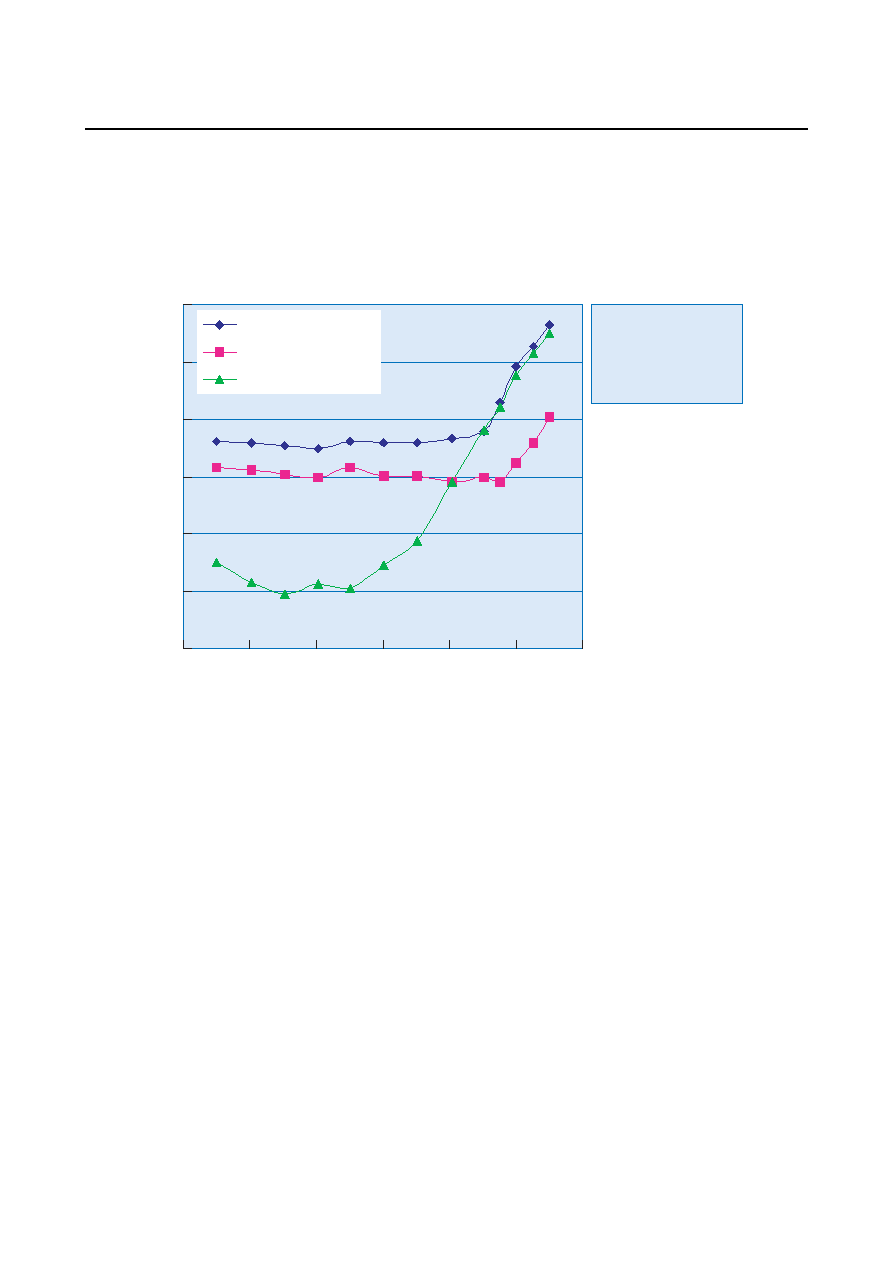
Adjacent Channel Leakage Power, Reverse IM3
f=1900 MHz
Vd1=Vd2=10 V
Vg1=Vg2=-5 V
RIM3:f2=f1+2.7MHz
Pin2=-10dBm
-90
-85
-80
-75
-70
-65
-60
24
26
28
30
32
34
36
Pout (dBm)
Padj600kHz offset
Padj900kHz offset
RIM3
Padj , RIM3 (dBc)

