D 281 S 60 T
Vorl‰ufige Daten
Preliminary Data
Hˆchstzul‰ssige Werte / Maximum rated values
Elektrische Eigenschaften / Electrical properties
Periodische Spitzensperrspannung
repetitive peak reverse voltage
t
vj
= -40∞C ... t
vj max
, f = 50Hz
V
RRM
6000 V
Durchlaþstrom-Grenzeffektivwert
RMS forward current
t
C
= 60∞C, f = 50Hz
I
FRMSM
610 A
Dauergrenzstrom
mean forward current
t
C
= 85∞C, f = 50Hz
I
FAVM
280 A
t
C
= 60∞C, f = 50Hz
390 A
Stoþstrom-Grenzwert
surge forward current
t
vj
= t
vj max
, t
p
= 10ms
I
FSM
5000
A
Grenzlastintegral
I2t-value
I
2
t
125 * 10
3
A
2
s
Period. Abklingsteilheit des Durchlaþstroms
beim Ausschalten
repetitive decay rate of on-state current at
turn-of
i
FM
= 1000A, v
R
= 1500 V
C
S
= 0.125µF, R
S
= 6
(-di
F
/dt)
com
1000 A/µs
Hˆchstzul‰ssige Kommutierungsspannung als
GTO Snubberdiode
maximum permissible link voltage as
GTO snubber-diode
i
F
100A, L
250nH, snubberless
V
R(cr)
4500 V
Charakteristische Werte / Characteristic values: Transistor
Gleichsperrspannung
continuous direct reverse voltage
failure rate
< 100, estimate value
V
R(D)
typ. 2900 V
Durchlaþspannung
forward voltage
t
vj
= t
vj max
, i
F
= 1200A
v
F
max. 5,0 V
Schleusenspannung
threshold voltage
t
vj
= t
vj max
,
V
(TO)
2,15 V
Ersatzwiderstand
forward slope resistance
t
vj
= t
vj max
,
r
T
2,38 m
Durchlaþrechenkennlinie
On-state characteristics for calculation
t
vj
= t
vj max
,
A
-2,29800
i
F
= 500A ... 3000A
B
0,00312
C
1,05600
D
-0,11300
Spitzenwert der Durchlaþverzˆgerungsspannungpeak value of forward recovery voltage
t
vj
= t
vj max
, di
F
/dt = 1000A/µs
V
FRM
typ. 280 V
Sperrstrom
reverse current
t
vj
= t
vj max
, v
R
= V
RRM
i
R
200 mA
R¸ckstromspitze
peak reverse recovery current
t
vj
= t
vj max
t
on
550 A
i
FM
= 1000A, -di
F
/dt = 250A/µs
v
R
= 1000V, C
S
= 0.125µF, R
S
= 6
Sperrverzˆgerungsladung
recovered charge
t
vj
= t
vj max
I
RM
max. 1300 µAs
i
FM
= 1000A, -di
F
/dt = 250A/µs
v
R
= 1000V, C
S
= 0.125µF, R
S
= 6
Thermische Eigenschaften / Thermal properties
Innerer W‰rmewiderstand
thermal resistance, junction to case
beidseitig / two-sided, DC
R
thJC
max. 0,035 ∞C/W
Anode / anode, DC
max. 0,070 ∞C/W
Kathode /cathode, DC
max. 0,070 ∞C/W
Ðbergangs-W‰rmewiderstand
thermal resistance, case to heatsink
K¸hlfl‰che / cooling surface
R
thCK
max. 0,006 ∞C/W
beidseitig / two-sided
max. 0,012 ∞C/W
einseitig / single sided
Hˆchstzul. Sperrschichttemperatur
max. junction temperature
T
vj max
125 ∞C
Betriebstemperatur
operating temperature
T
c op
-40...+125 ∞C
Lagertemperatur
storage temperature
T
stg
-40...+150 ∞C
Mechanische Eigenschaften / Mechanical properties
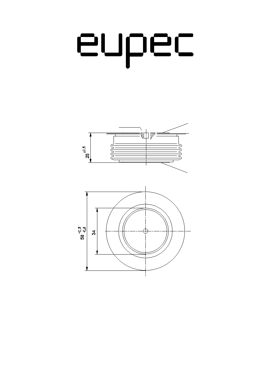
Si-Element mit Druckkontakt
Si-pellet with pressure contace
38DS60
Anpreþkraft
clamping force
F
10...16 kN
Gewicht
weight
G
typ. 250 g
Kriechstrecke
creepage distance
30 mm
Luftstrecke
air distance
ca. 20 mm
Feuchteklasse
humidity classification
DIN 40040
C
Schwingfestigkeit
vibration resistance
f = 50Hz
50 m/s
2
Mit dieser technischen Information werden Halbleiterbauelemente spezifiziert, jedoch keine Eigenschaften zugesichert. Sie gilt in Verbindung mit den
zugehˆrigen Technischen Erl‰uterungen. This technical information specifies semiconductor devices but promises no characteristics. It is valid in
combination with the belonging technical notes.
(
)
V
A B i
C
i
D
i
F
F
F
F
=
+
+
+ +
ln
1

D 281 S
D 281 S 60 T / 1
0
500
1000
1500
2000
2500
3000
3500
0
1
2
3
4
5
6
7
8
9
10
Pos. n
1
2
3
4
5
R
thn
[∞C/W]
n
[s]
Analytical elements of transient thermal impedance Z
thJC
per arm for DC
Analytical function:
n
max
n=1
Z
thJC
= R
thn
(1-e )
t
-
n
Double side cooled
Pos. n
1
2
3
4
5
R
thn
[∞C/W]
n
[s]
Anode side or Cathode side colled
D 281 S 60 T / 2
D 281 S 60 T / 3
D 281 S 60 T / 4
D 281 S 60 T / 5
i
F
[A]
I
rm
[A]
Z
thJC
[K/W]
V
FRM
[V]
v
F
[V]
t
[s]
Bild / Fig. 1
On-State Characteristics (v
F
)
typical and upper limit of scatter range
t
vj
= 125∞C
Bild / Fig. 3
Transient thermal Impedance for constant-current
Bild / Fig. 5
Reverse Recovery Charge I
rm
= f (-di/dt)
Upper limit of scatter range
Conditions: t
vj
= 125∞C
V
r
= 1000V
RC Snubber 6
, 0.125µF
Parameter: I
f
Bild / Fig. 2
Typical Peak Forward Recovery Voltage V
FRM
= f (di
F
/dt)
linear di/dt
Parameter t
vj
Bild / Fig. 4
Reverse Recovery Charge Q
rr
= f (-di/dt)
Upper limit of scatter range
Conditions: t
vj
= 125∞C
V
r
= 1000V
RC Snubber 6
, 0.125µF
Parameter: I
f
0,0119
0,014
0,0049
0,0033
0,0009
0,035
1,28
0,13
0,024
0,0044
0,0012
-
0,0463
0,0146
0,0049
0,0033
0,0009
0,07
5,37
0,134
0,024
0,0044
0,0012
-
0
500
1000
1500
0
100
200
300
400
500
600
di/dt [A/µs]
2500 A
500 A
1000A
100 A
0,001
0,01
0,1
1
10
100
Double side
Cathode side
0
0,1
0,01
0,02
0,03
0,04
0,05
0,06
0,08
0,09
Anode side or
0
100
450
500
50
200
350
400
150
300
250
0
200
400
600
800
1000
1200
1600
2000
1400
1800
25∞C
125∞C
di/dt [A/µs]
max.
typ.
Q
rr
[µAs]
100 A
2500 A
1000A
500 A
0
500
1000
1500
2000
2500
3000
100
200
300
400
500
600
di/dt [A/µs]
0