
Schnelle Gleichrichterdiode
Fast Diode
D 721 S 45 T
Elektrische Eigenschaften / Electrical properties
Hˆchstzul‰ssige Werte / Maximum rated values
Periodische Spitzensperrspannung
3500 V, 4000V
repetitive peak reverse voltage
t
vj
= -40∞C...125∞C
V
RRM
4500 V
Stoþspitzensperrspannung
3600 V, 4100V
non-repetitive peak reverse voltage
t
vj
= +25∞C...125∞C
V
RSM
4600 V
Durchlaþstrom-Grenzeffektivwert / RMS forward current
I
FRMSM
1700 A
Dauergrenzstrom / mean forward current
t
C
= 85∞C
I
FAVM
720 A
t
C
= 52∞C
1080 A
Stoþstrom-Grenzwert
1)
t
vj
= 25∞C
I
FSM
16000 A
surge forward current
1)
t
vj
= 125∞C
15000 A
Grenzlastintegral
t
vj
= 25∞C
I≤t
1,3x10
6
A≤s
I≤t-value
t
vj
= 125∞C
1,13x10
6
A≤s
Kritische periodische Ausschaltstromsteilheit
t
vj
= 125∞C, I
FM
= 2000 A, V
R
= 3000 V
(-di/dt)
com
500 A/µs
critical repetitive rate of fall of on - state
C = 0,25 µF, R = 6
Charakteristische Werte / Characteristic values
Gleichsperrspannung / cont. direct reverse voltage
t
c
= -40∞C ... +85∞C
V
R(D)
typ. 2000 V
Durchlaþspannung / forward voltage
t
vj
= 125∞C i
FM
= 2500 A
V
F
3,5 V
Schleusenspannung / threshold voltage
t
vj
= 125∞C
V
(TO)
1,7 V
Ersatzwiderstand / forward slope resistance
t
vj
= 125∞C
r
T
0,69 m
Sperrstrom / reverse current
t
vj
= 125∞C, v
R
= 0,67 V
RRM
i
R
ca. 75 mA
t
vj
= 125∞C, v
R
= V
RRM
140 mA
1)
R¸ckstromspitze / peak reverse recovery current
i
FM
= 1000 A, -di
F
/dt = 250 A/µs
I
RM
600 A
t
vj
= 125 ∞C; v
R
= 1000 V;
C = 0,25 µF; R = 6
Sperrverzˆgerungsladung
i
FM
= 1000 A, -di
F
/dt = 250 A/µs
Q
rr
1700 µAs
recovered charge
t
vj
= 125 ∞C; v
R
= 1000 V;
C = 0,25 µF; R = 6
Thermische Eigenschaften / Thermal properties
Innerer W‰rmewiderstand
K¸hlfl‰che / cooling surface
R
thJC
thermal resistance, junction to case
beidseitig / two-sided
0,018 K/W
Anoden / anode
0,033 K/W
Kathode / cathode
0,04 K/W
Ðbergangs-W‰rmewiderstand
K¸hlfl‰che / cooling surface
R
thCK
thermal resistance, case to heatsink
beidseitig / two-sided
0,005 K/W
einseitig / single-sided
0,01 K/W
Hˆchstzul. Sperrschichttemp. / max. junction temperat.
t
vj
max
125 ∞C
Betriebstemperatur / operating temperature
t
c
op
-40...+125 ∞C
Lagertemperatur / storage temperature
t
stg
-40...+150 ∞C
Mechanische Eigenschaften / Mechanical properties
Geh‰use, siehe Anlage / case, see appendix
Seite / page 1
Anpreþkraft /clamping force
F
15...36 kN
Gewicht / weight
G
ca. 600 g
Luftstrecke / air distance
ca. 20 mm
Kriechstrecke / creepage distance
30 mm
Feuchteklasse / humidity classification
DIN 40040
C
Schwingfestigkeit / vibration resistance
f = 50 Hz
50 m/s≤
Mit dieser technischen Information werden Halbleiterbauelemente spezifiziert, jedoch keine Eigenschaften zugesichert. Sie gilt
in Verbindung mit den zugehˆrigen Technischen Erl‰uterungen.
This technical information specifies semiconductor devices but promises no characteristics. It is valid in combination with the
belonging technical notes.
1) Richtwert f¸r obere Streubereichsgrenze / Upper limit of scatter range (standart value)

Fig. 1
On-state characteristic i
F
= f(V
F
)
t
vj
= 125∞C
Upper limit of scatter range
Lower limit of scatter range
Fig. 2
On-state losses (average values)
I
F
= f(P
FAV
)
t
vj
= 125 ∞C
D 721 S
D 721 S_01
1,0
1,5
2,0
2,5
3,0
3,5
4,0
4,5
4000
3000
2000
1000
0
i
F
[A]
v
F
[V]
4000
3500
3000
2500
2000
1500
1000
500
0
500
1000
1500
2000
2500
D 721 S_02
90% 80% 70%
100%
60%
50%
40%
30%
20%
10%
5%
I
F
[A]
P
FAV
[W]
0
0,001
0,01
0,1
1
10
100
D 721 S_03
0,06
0,05
0,04
0,03
0,02
0,01
3
2
1
2 3 4 6 8
2 3 4 6 8
2 3 4 6 8
2 3 4 6 8
2 3 4 6 8
t [s]
Z
thJC
[K/W]
Analytical elements of transient thermal impedance Z
thJC
for DC
Analytical function:
Z
th
JC =
R
thn
(1-EXP(-t/
n
))
n
max
n = 1
Fig. 3
Transient thermal impedance Z
thJC
= f(t), DC
1 - Two-sided cooling
2 - Anode-sided cooling
3 - Cathode-sided cooling
1. Z
thJC
2. Z
thJC
3. Z
thJC
r [K/W]
[s]
r [K/W]
[s]
r [K/W]
[s]
1 0,00637 1,80000 0,02137 8,00000 0,02837 6,80000
2 0,00904 0,14000 0,00904 0,14000 0,00904 0,14000
3 0,00267 0,01410 0,00167 0,01410 0,00167 0,01410
4 0,00080 0,00265 0,00080 0,00265 0,00080 0,00265
5 0,00012 0,00067 0,00012 0,00067 0,00012 0,00067
0,00180
-
0,03300
-
0,04000
-
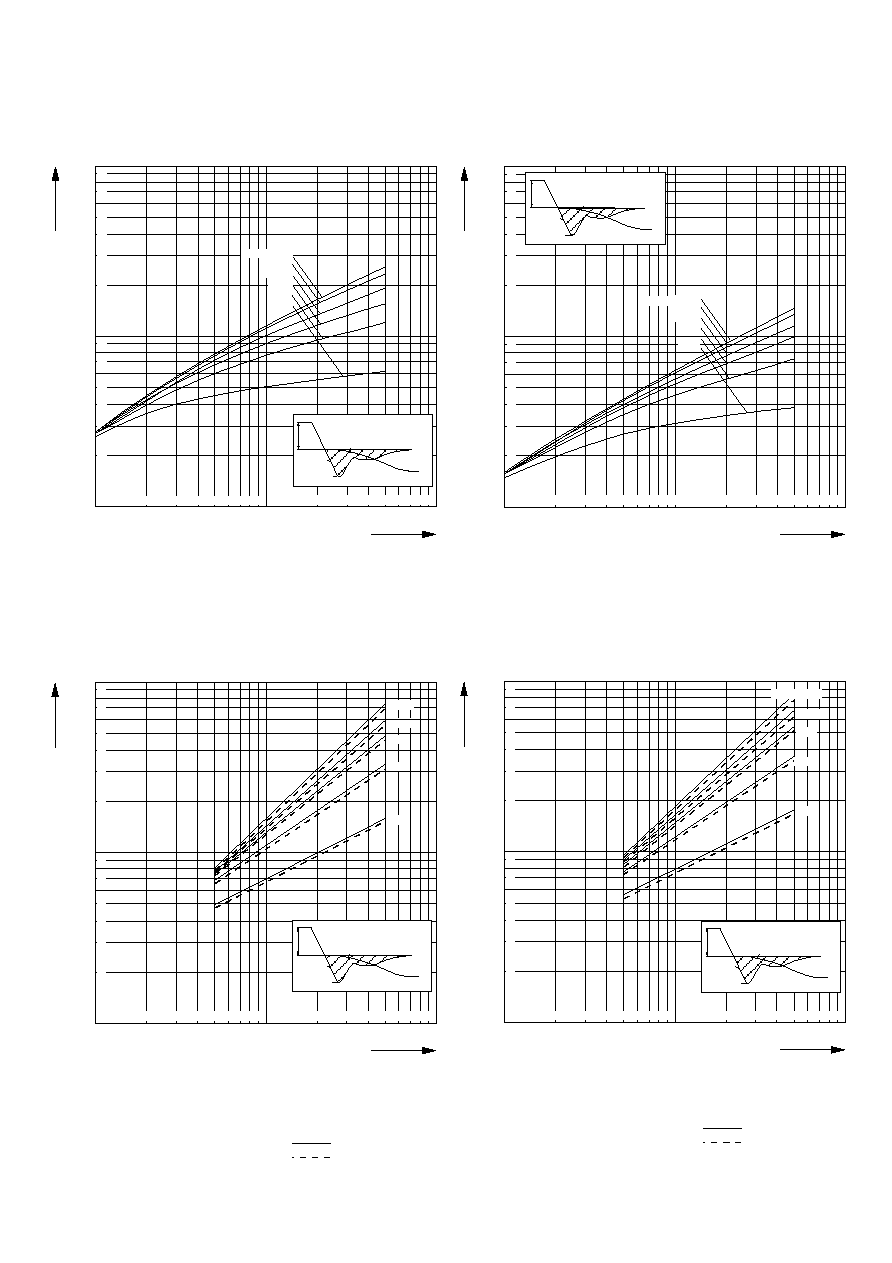
Fig. 11
Turn-off-losses E
off
= f(di/dt)
diodes with V
F
max
Application: GTO-freewheeling diode
Parameter:I
FM
; Snubberdiode D 291 S
t
vj
= 125∞C; C
S
= 4 µF f¸r v
R
V
RM
C
S
= 24 µF f¸r v
R
V
RM
L
S
= 0,2 µH
D 721 S
V
R(Spr)
= 3000 V
V
R(Spr)
= 2000 V
1000
100
10
10
100
1000
D 721 S_08
I
FM
= 3000A
2000A
1000A
600A
300A
100A
3
4
5
7
9
2
2
3
4
5
7
9
2
3
4
5 6 7 8 9
2
3
4
5 6 7 8 9
-di/dt [A/µs]
Q
rr
[µAs]
-di/dt
I
RM
Q
rr
V
R
I
FM
1000
100
10
10
100
1000
D 721 S_09
2
3
4
5 6 7 8 9
2
3
4
5 6 7 8 9
2
3
4
5
7
9
2
3
4
5
7
9
Q
rr
[µAs]
-di/dt [A/µs]
-di/dt
I
RM
Q
rr
V
R
I
FM
I
FM
= 3000A
2000A
1000A
600A
300A
100A
10
1
0,1
10
100
1000
D 721 S_11
2
3
4
5 6 7 8 9
2
3
4
5 6 7 8 9
2
3
4
5
7
9
2
3
4
5
7
9
I
FM
= 3000A
1000A
600A
300A
100A
E
off
[Ws]
-di/dt [A/µs]
-di/dt
I
RM
Q
rr
V
R
I
FM
V
R(Spr)
V
R(Spr)
= 3000 V
V
R(Spr)
= 2000 V
Fig. 8
Reverse recovery charge (upper limit, ca. 98% values)
Application: GTO-freewheeling diode
Parameter: I
FM
t
vj
125∞C; C
S
4µF
R
S
= 0
;
V
R
> 2000 V ... 3000 V
Fig. 9
Reverse recovery charge (lower limit, ca. 2% values)
Application: GTO-freewheeling diode
Parameter: I
FM
t
vj
125∞C; C
S
4µF
R
S
= 0
;
V
R
> 2000 V ... 3000 V
10
1
0,1
10
100
1000
D 721 S_13
3000A
1000A
600A
300A
100A
E
off
[Ws]
-di/dt [A/µs]
-di/dt
I
RM
Q
rr
V
R
I
FM
V
R(Spr)
2
3
4
5 6 7 8 9
2
3
4
5 6 7 8 9
2
3
4
5
7
9
2
3
4
5
7
9
V
R(Spr)
= 3000 V
V
R(Spr)
= 2000 V
Fig. 10
Turn-off-losses E
off
= f(di/dt)
diodes with V
F
max
Application: GTO-freewheeling diode
Parameter:I
FM
; Snubberdiode D 291 S
t
vj
= 125∞C; C
S
= 6 µF f¸r v
R
V
RM
C
S
= 36 µF f¸r v
R
V
RM
L
S
= 0,2 µH

