T
188 F
Elektrische Eigenschaften Electrical properties
Hˆchstzul‰ssige Werte Maximum rated values
Periodische Vorw‰rts- und
R¸ckw‰rts-Spitzensperrspannung
repetitive peak forward off-state
and reverse voltages
Vorw‰rts-Stoþspitzen- non repetitive peak
sperrspannung forward off-state voltage
R¸ckw‰rts-Stoþspitzen- non repetitive peak
sperrspannung reverse voltage
Durchlaþstrom-Grenzeffektivwert RMS on-state current
Dauergrenzstrom average on-state current
Stoþstrom-Grenzwert
Grenzlastintegral
Kritische Stromsteilheit
surge current
critical rate of rise of on-state current
Kritische Spannungssteilheit critical rate of rise of off-state voltage
= - 4 0 ∞ C
1300"
V
DSM =
V
V
V
V
RSM =
+
100 V
400
188
254
3300
2900
54500
42000
160
50 50
500 500
500 50
1000 500
A
A
A
A
A
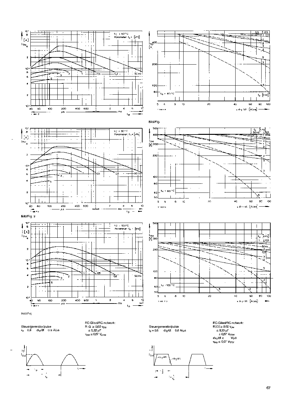
tc = 64∞C
10
=
= 10
t,
10
=
t
67%
f = 50 Hz
A,
=
=
= 67%
B:
L:
Charakteristische Werte Characteristic values
Durchlaþspannung
Schleusenspannung
Ersatzwiderstand
Z¸ndstrom
Z¸ndspannung
Nicht z¸ndender Steuerstrom
Nicht z¸ndende Steuerspannung
Haltestrom
Einraststrom
Vorw‰rts- u. R¸ckw‰rts-Sperrstrom
Z¸ndverzug
Freiwerdezeit
on-state voltage
threshold voltage
slope resistance
gate trigger current
gate trigger voltage
gate non-trigger current
gate non-trigger voltage
holding current
latching current
forward off-state and reverse Currents
gate controlled delay time
circuit commutated turn-off time
600 A
=
=
12 V
=
= 12 V
=
=
12
= 10
12
10
= 20
=
=
=
A,
=
siehe Techn.
Techn. Inf.
VT
max.
V
v
150 mA
2 v
10 mA
V
250 mA
1 A
max.
max.
max.
max.
max.
max.
max. 30 mA
max.
t ,
s :
max. 18 us
E: max. 20
F: max. 25
Thermische Eigenschaften
Innerer W‰rmewiderstand
f¸r beidseitige K¸hlung
Thermal
thermal resistance, junction to case
for two-sided cooling
for anode-sided cooling
for cathode-sided cooling
thermal resistance, case to heatsink
max. junction temperature
Operating temperature
storage temperature
f¸r anodenseitige K¸hlung
f¸r kathodenseitige K¸hlung
Ðbergangsw‰rmewiderstand
Hˆchstzul. Sperrschichttemperatur
Betriebstemperatur
Lagertemperatur
0,166
125∞C
125∞C
+ 140∞C
sin
DC
= 180" sin
DC
160" sin
DC
beidseitig/two-sided
einseitiglone-sided
max.
max.
max.
max.
max.
max.
max.
max.
t
t
Mechanische Eigenschaften Mechanical properties
Si-Element mit Druckkontakt Si-pellet with pressure contact
Anpreþkraft Clamping force
Gewicht weight
Kriechstrecke Creepage distance
Feuchteklasse humidity classification
DIN 40040
Schwingfestigkeit Vibration resistance
Maþbild outline
DIN
l
F¸r grˆþere St¸ckzahlen bitte Liefertermin erfragen/Delivery for larger quantities on request
F
G
70 g
17mm
C
50
Seitelpage 154
1) Werte nach DIN IEC 747-6 (ohne vorausgehende Kommutierung)/Values to DIN IEC 747-6 (without prior commutation)
2) Unmittelbar nach der Freiwerdezeit, vgl. Meþbedingungen f¸r
after circuit commutated turn-off time, see Parameters
66

T 188 F
Blld/Fig. 16
Bild/Fig. 16
R¸ckstromspitze
=
=
=
=
Peak reverse recovery current
=
= 0.5
= 0.8
Parameter: DurchlaþstromlOn-state current
Z¸ndverzug/Gate controlled delay time
=
=
Maximaler
Characteristic
b Typischer
Characteristic
Blld/Flg. 17
Transienter innerer W‰rmewiderstand
= f(t), DC
Transient thermal impedance
= f(t), DC
1 Beidseitige K¸hlung/two-sided cooling
2 Anodenseitige K¸hlunglanode side cooling
3 Kathodenseitige K¸hlung/cathode side cooling
BildlFig. 19
Steuercharakteristik mit Z¸ndbereichenlGate Characteristic with triggering
= 12 V
Parameter:
b
SteuerimpulsdauenTrigger pulse duration
10 1
Hˆchstzul‰ssige Spitzensteuerverlustleistung/
Max. rated peak gate power dissipation
20 40 60
Analytische Elemente des transienten W‰rmewiderstandes
f¸r DC
Analytical elements of
thermal impedance
for DC
Analytische Funktion/analytical function:
omax
Z
=