 | –≠–ª–µ–∫—Ç—Ä–æ–Ω–Ω—ã–π –∫–æ–º–ø–æ–Ω–µ–Ω—Ç: T2561N | –°–∫–∞—á–∞—Ç—å:  PDF PDF  ZIP ZIP |

Technische Information / Technical Information
Netz Thyristor
Phase Control Thyristor
T 2561N 75...80TOH
.
BIP AM / SM PB 2001-05-04, Przybilla J. / Keller
Release 3
Seite/page
N
1
Features:
Volle Sperrf‰higkeit bei 125∞ mit 50 Hz
Full blocking capability at 125∞C with 50 Hz
Hohe Stoþstrˆme und niedriger W‰rme-
High surge currents and low thermal resistance
widererst‰nde durch NTV-Verbindung
by using low temperature-connection NTV between
zwischen Silizium und Mo-Tr‰gerscheibe.
silicon wafer and molybdenum.
Elektroaktive Passivierung durch a - C:H
Electroactive passivation by a - C:H
Elektrische Eigenschaften / Electrical properties
Hˆchstzul‰ssige Werte / Maximum rated values
Periodische Vorw‰rts - und R¸ckw‰rts - Spitzensperrspannung
repetitive peak forward off-state and reverse voltage
f = 50 Hz
V
DRM
,
V
RRM
t
vj min
= -40∞C t
vj min
= 0∞C
7500 7700
8000 8200
V
V
Durchlaþstrom-Grenzeffektivwert
RMS forward current
I
TRMSM
5600 A
Dauergrenzstrom
mean forward current
t
C
= 85∞C, f = 50Hz
t
C
= 60∞C, f = 50Hz
I
TAVM
2560
3570
A
A
Stoþstrom-Grenzwert
surge forward current
t
vj
= 25∞C, t
p
= 10ms, V
R
= 0
t
vj
= t
vj max
, t
p
= 10ms, V
R
= 0
I
TSM
63
56
kA
kA
Grenzlastintegral
I
2
t-value
t
vj
= 25∞C, t
p
= 10ms
t
vj
= t
vj max
, t
p
= 10ms
I
2
t
19,8∑10
6
15,7∑10
6
A
2
s
A
2
s
Kritische Stromsteilheit
critical rate of rise of on-state current
DIN IEC 747-6
f = 50Hz, v
D
= 0,67 V
DRM
i
GM
= 3A, di
G
/dt = 6A/µs
(di/dt)
cr
300 A/µs
Kritische Spannungssteilheit
critical rate of rise of off-state current
t
vj
= t
vj max
, v
D
= 0,67 V
DRM
5. Kennbuchstabe / 5 th letter H
(dv/dt)
cr
2000 V/µs

Technische Information / Technical Information
Netz Thyristor
Phase Control Thyristor
T 2561N 75...80TOH
.
BIP AM / SM PB 2001-05-04, Przybilla J. / Keller
Release 3
Seite/page
N
2
Elektrische Eigenschaften / Electrical properties
Charakteristische Werte / Characteristic values
Durchlaþspannung
on-state voltage
t
vj
= t
vj max
, i
T
= 6kA
v
T
typ
2,75
max
2,95
V
Schleusenspannung / threshold voltage
Ersatzwiderstand / slope resistance
t
vj
= t
vj max
V
(TO)
r
T
typ
1,23
0,253
max
1,28
0,278
V
m
Durchlaþrechenkennlinien
500 A
i
T
6000 A
On - state characteristics for calculation
( )
V
A B i
C
i
D
i
T
T
T
T
= + +
+ +
ln
1
t
vj
= t
vj max
A
B
C
D
typ
-0,00607
0,000181
0,162
0,00342
max
-0,00503
0,000187
0,16
0,0057
Z¸ndstrom
gate trigger current
t
vj
= 25∞C, v
D
= 6V
I
GT
350 mA
Z¸ndspannung
gate trigger voltage
t
vj
= 25∞C, v
D
= 6V
V
GT
2,5 V
Nicht z¸ndender Steuerstrom
gate non-trigger current
t
vj
= t
vj max
, v
D
= 6V
t
vj
= t
vj max
, v
D
= 0,5
V
DRM
I
GD
20
10
mA
mA
nicht z¸ndende Steuerspannung
gate non-trigger voltage
t
vj
= t
vj max
, v
D
= 0,5
VDRM
V
GD
0,4 V
Haltestrom
holding current
t
vj
= 25∞C, v
D
= 12V, R
A
= 4,7
I
H
350 mA
Einraststrom
latching current
t
vj
= 25∞C, v
D
= 12V, R
GK
10
i
GM
= 3A, di
G
/dt= 6 A/µs, t
g
= 20µs
I
L
3 A
Vorw‰rts- und R¸ckw‰rts-Sperrstrom
forward off-state and reverse currents
t
vj
= t
vj max
v
D
= V
DRM
, v
R
= V
RRM
i
D
, i
R
900 mA
Z¸ndverzug
gate controlled delay time
DIN IEC 747-6
t
vj
= 25∞C,
i
GM
= 3A, di
G
/dt = 6A/µs
t
gd
2,5 µs
Freiwerdezeit
circuit commutated turn-off time
t
vj
= t
vj max
, i
TM
= I
TAVM
v
RM
= 100V, v
DM
= 0,67 V
DRM
dv
D
/dt = 20V/µs, -di
T
/dt = 10A/µs
4. Kennbuchstabe / 4 th letter O
t
q
typ
550 µs
Sperrverzˆgerungsladung
recovered charge
t
vj
= t
vj max
I
TM
= 2,5 kA, di/dt = 10 A/µs
V
R
= 0,5 V
RRM
, V
RM
= 0,8 V
RRM
Q
r
22 mAs
R¸ckstromspitze
peak reverse recovery current
t
vj
= t
vj max
I
TM
= 2,5 kA, di/dt = 10 A/µs
V
R
= 0,5 V
RRM
, V
RM
= 0,8 V
RRM
I
RM
400 A

Technische Information / Technical Information
Netz Thyristor
Phase Control Thyristor
T 2561N 75...80TOH
.
BIP AM / SM PB 2001-05-04, Przybilla J. / Keller
Release 3
Seite/page
N
3
Thermische Eigenschaften / Thermal properties
Innerer W‰rmewiderstand
thermal resistance, junction to case
beidseitig / two-sided, = 180∞sin
beidseitig / two-sided , DC
Anode / anode
DC
Kathode / cathode
DC
R
thJC
0,0046
0,0043
0,0075
0,01
∞C/W
∞C/W
∞C/W
∞C/W
Ðbergangs-W‰rmewiderstand
thermal resistance, case to heatsink
beidseitig / two-sided
einseitig / single-sided
R
thCK
0,001
0,002
∞C/W
∞C/W
Hˆchstzul‰ssige Sperrschichttemperatur
max. junction temperature
t
vj max
125 ∞C
Betriebstemperatur
operating temperature
t
c op
-40...+125 ∞C
Lagertemperatur
storage temperature
t
stg
-40...+150 ∞C
Mechanische Eigenschaften / Mechanical properties
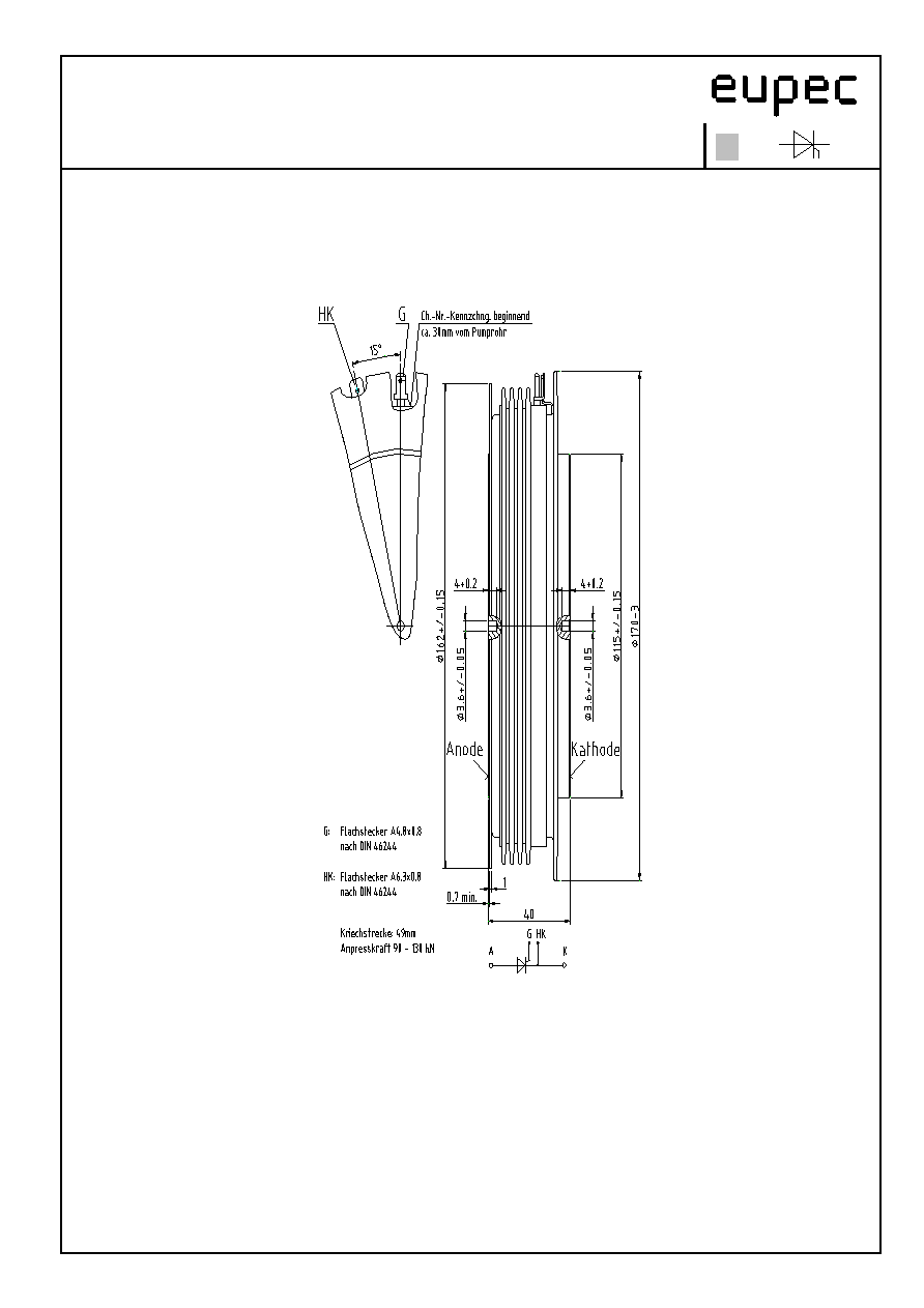
Geh‰use, siehe Anlage
case, see appendix
Seite 4
Si-Element mit Druckkontakt, Amplifying-Gate
Si-pellet with pressure contact, amplifying gate
119TN80
Anpreþkraft
clampig force
F
90...130 KN
Gewicht
weight
G
typ
4000 g
Kriechstrecke
creepage distance
49 mm
Feuchteklasse
humidity classification
DIN 40040
C
Schwingfestigkeit
vibration resistance
f = 50Hz
50 m/s
2
Mit dieser technischen Information werden Halbleiterbauelemente spezifiziert, jedoch keine Eigenschaften zugesichert. Sie gilt in Verbidung mit den zugehˆrigen technischen Erl‰uterungen.
This technical Information specifies semiconductor devices but promises no characteristics. It is valid in combination with the belonging technical notes.
Technische Information / Technical Information
Netz Thyristor
Phase Control Thyristor
T 2561N 75...80TOH
.
BIP AM / SM PB 2001-05-04, Przybilla J. / Keller
Release 3
Seite/page
N
4
Maþbild / Outline
Technische Information / Technical Information
Netz Thyristor
Phase Control Thyristor
T 2561N 75...80TOH
.
BIP AM / SM PB 2001-05-04, Przybilla J. / Keller
Release 3
Seite/page
N
5
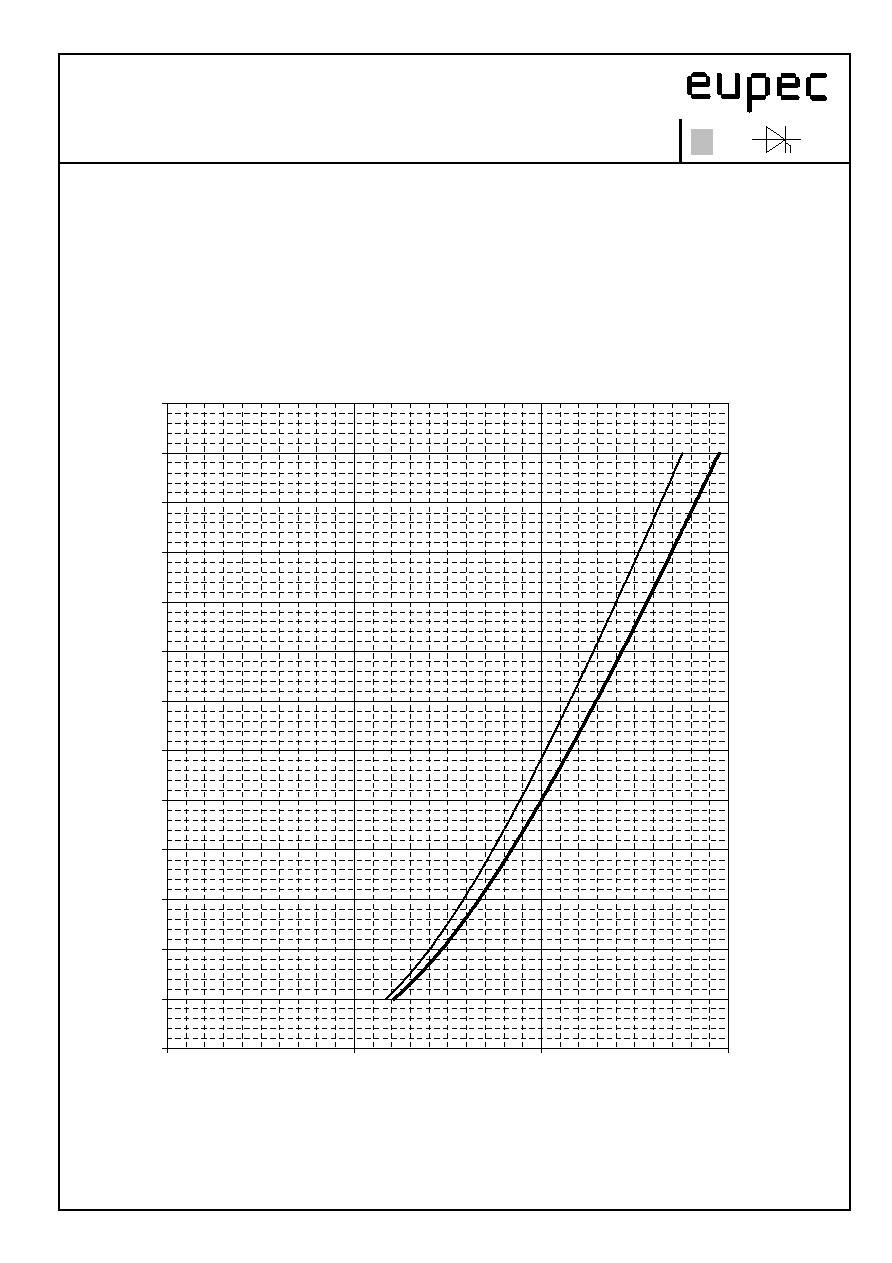
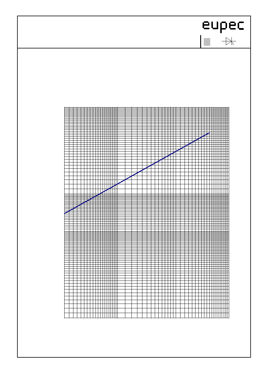
Durchlaþkennlinie i
T
= f ( v
T
)
Limiting and typical on-state characteristic
t
vj
= 125
∞
∞
∞
∞ C
0
500
1000
1500
2000
2500
3000
3500
4000
4500
5000
5500
6000
6500
0
1
2
3
V
T
[V]
I
T
(
A
)
typ max
Technische Information / Technical Information
Netz Thyristor
Phase Control Thyristor
T 2561N 75...80TOH
.
BIP AM / SM PB 2001-05-04, Przybilla J. / Keller
Release 3
Seite/page
N
6
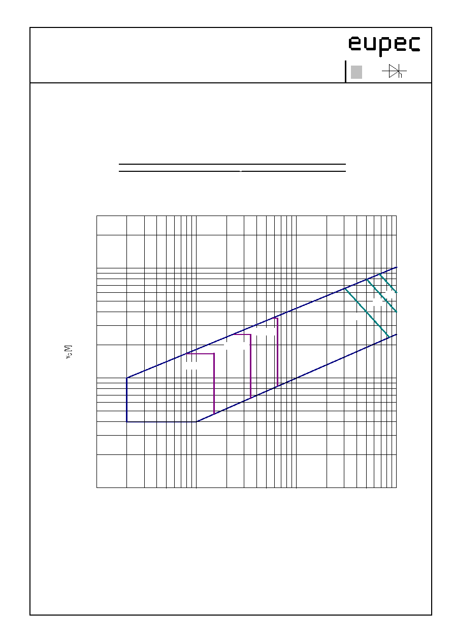
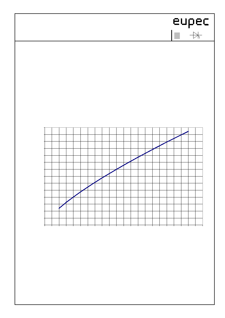
Steuerkreischarakteristik mit Z¸ndbereichen
Gate characteristic with triggering areas
v
G
= f (i
G
), V
D
= 6V
Parameter a b c
Steuerimpulsdauer / trigger pulse duration t
g
(ms) 10 1 0,5
Hˆchstzul‰ssige Spitzensteuerverlustleistung
Max. rated peak power dissipation
P
GM
(W)
20
40
60
3 0
2 0
1 0
5
2
1
0 , 5
0 , 2
1 0
1 0 0 0 0
5 0 0 0
2 0 0 0
5 0
2 0
1 0 0
2 0 0
5 0 0
1 0 0 0
i
G
[ m A ]
+ 1 2 5 ∞ C
+ 2 5 ∞ C
- 4 0 ∞ C
a
b
c
Technische Information / Technical Information
Netz Thyristor
Phase Control Thyristor
T 2561N 75...80TOH
.
BIP AM / SM PB 2001-05-04, Przybilla J. / Keller
Release 3
Seite/page
N
7
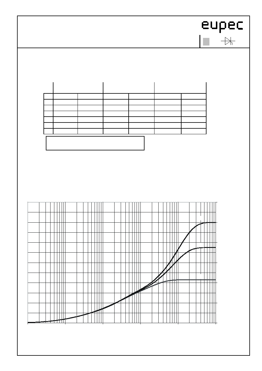
Transienter innerer W‰rmewiderstand
Transient thermal impedance Z
(th)JC
= f (t)
doppelseitige
K¸hlung
anodenseitige
K¸hlung
kathodenseitige
K¸hlung
r [K/W]
[s]
r [K/W]
[s]
r [K/W]
[s]
1 0,00183
1,9
0,00465
7,5
0,00715
10,2
2 0,00132
0,3
0,00052
0,85
0,00052
0,85
3 0,00075
0,065
0,00157
0,225
0,00157
0,225
4 0,00038
0,011
0,00054
0,029
0,00054
0,029
5 0,00002
0,003
0,00022
0,0075
0,00022
0,0075
0,0043
-
0,0075
-
0,01
-
(
)
Z
R
e
thJC
thn
t
n
n
n
=
-
-
=
1
1
/
m ax
0
0,002
0,004
0,006
0,008
0,01
0,012
0,001
0,01
0,1
1
10
100
t / [sec.]
Z
(th
)
J
C
/
[K
/
W
]
d
a
Technische Information / Technical Information
Netz Thyristor
Phase Control Thyristor
T 2561N 75...80TOH
.
BIP AM / SM PB 2001-05-04, Przybilla J. / Keller
Release 3
Seite/page
N
8
Sperrverzˆgerungsladung Q
r
= f ( - di/dt )
recovered charge
t
vj
= 125
∞C, I
TM
= 2500A,v
R
= 0,5 V
RRM
, v
RM
= 0,8 V
RRM
9
8
7
6
50
40
30
20
10
5
4
3
2
30
20
10
9
8
7
6
5
4
3
2
1
di/dt [A /µs]
Q
rr
[m As]
Technische Information / Technical Information
Netz Thyristor
Phase Control Thyristor
T 2561N 75...80TOH
.
BIP AM / SM PB 2001-05-04, Przybilla J. / Keller
Release 3
Seite/page
N
9
R¸ckstromspitze / reverse recovery current
(typische Abh‰ngigkeit / typical dependence)
I
RM
= f (di/dt)
t
vj
= 125
∞C, I
TM
= 2500A, v
R
= 0,5
V
RRM
, v
RM
= 0,8
V
RRM
0
50
100
150
200
250
300
350
400
450
500
550
600
650
700
0
1
2
3
4
5
6
7
8
9
10
11
12
13
14
15
16
17
18
19
20
21
22
d i / d t [A / µs]
I
RM
[A
]