
T 2709 N
Elektrische Eigenschaften
Electrical properties
Hˆchstzul‰ssige Werte
Maximum rated values
Periodische
Vorw‰rts-
und
R¸ckw‰rts-Spitzensperrspannung
repetitive peak forward off-state and
reverse voltages
t
vj
= -40∞C...t
vj max
V
DRM
, V
RRM
1600
1800
2000 2200
V
Vorw‰rts-
Stoþspitzensperrspannung
non-repetitive peak forward off-state
voltage
t
vj
= -40∞C...t
vj max
V
DSM
1600
1800
2000 2200
V
R¸ckw‰rts-
Stoþspitzensperrspannung
non-repetitive peak reverse voltage
t
vj
= +25∞C...t
vj max
V
RSM
1700
1900
2100 2300
V
Durchlaþstrom-Grenzeffektivwert
RMS on-state current
I
TRMSM
5800 A
Dauergrenzstrom
average on-state current
t
c
= 85∞C
I
TAVM
2709 A
t
c
= 61∞C
3700 A
Stoþstrom-Grenzwert
surge current
t
vj
= 25∞C, t
p
= 10 ms
I
TSM
54000 A
1
)
t
vj
= t
vj max
, t
p
= 10 ms
50000 A
1
)
Grenzlastintegral
I
2
t-value
t
vj
= 25∞C, t
p
= 10 ms
I
2
t
14,58 ∑ 10
6
A
2
s
t
vj
= t
vj max
, t
p
= 10 ms
12,5 ∑ 10
6
A
2
s
Kritische Stromsteilheit
critical rate of rise of on-state current
DIN IEC 747-6, f = 50 Hz
(di
T
/dt)
cr
200 A/µs
I
GM
= 1 A, di
G
/dt = 1 A/µs
Kritische Spannungssteilheit
critical rate of rise of off-state voltage
t
vj
= t
vj max
, v
D
= 0,67 V
DRM
(dv
D
/dt)
cr
5.Kennbuchstabe/5th letter F
1000 V/µs
Charakteristische Werte
Characteristic values
Durchlaþspannung
on-state voltage
t
vj
= t
vj max
, i
T
= 11000 A
v
T
max. 2,35 V
Schleusenspannung
threshold voltage
t
vj
= t
vj max
V
T(TO)
0,9 V
Ersatzwiderstand
slope resistance
t
vj
= t
vj max
r
T
0,125 m
Z¸ndstrom
gate trigger current
t
vj
= 25 ∞C, v
D
= 6 V
I
GT
max. 250 mA
Z¸ndspannung
gate trigger voltage
t
vj
= 25 ∞C, v
D
= 6 V
V
GT
max. 2 V
Nicht z¸ndender Steuerstrom
gate non-trigger current
t
vj
= t
vj max
, v
D
= 6 V
I
GD
max. 10 mA
t
vj
= t
vj max
, v
D
= 0,5 V
DRM
max. 5 mA
Nicht z¸ndende Steuerspannung
gate non-trigger voltage
t
vj
= t
vj max
, v
D
= 0,5 V
DRM
V
GD
max. 0,25 V
Haltestrom
holding current
t
vj
= 25 ∞C, v
D
= 6 V, R
A
= 5
I
H
max. 300 mA
Einraststrom
latching current
t
vj
= 25 ∞C,v
D
= 6 V, R
GK
> = 10
I
L
max. 1500 mA
i
GM
= 1 A, di
G
/dt = 1 A/µs, t
g
= 20 µs
Vorw‰rts- und R¸ckw‰rts-Sperrstrom forward off-state and reverse currents
t
vj
= t
vj max
i
D
, i
R
max. 250 mA
v
D
= V
DRM
, v
R
= V
RRM
Z¸ndverzug
gate controlled delay time
DIN IEC 747-6, t
vj
= 25∞C
t
gd
max. 4 µs
i
GM
= 1 A, di
G
/dt = 1 A/µs
Freiwerdezeit
circuit commutated turn-off time
t
vj
= t
vj max
, i
TM
= I
TAVM
t
q
v
RM
= 100 V, v
DM
= 0,67 V
DRM
-di
T
/dt = 20 A/µs, -di
T
/dt=10A/µs
4.Kennbuchstabe/4th letter O
typ. 300 µs
Thermische Eigenschaften
Thermal properties
Innerer W‰rmewiderstand
thermal resistance, junction
K¸hlfl‰che/cooling surface
R
thJC
to case
beidseitig/two-sided,
=180∞ sin
max. 0,0085 ∞C/W
beidseitig/two-sided, DC
max. 0,0078 ∞C/W
Ðbergangs-W‰rmewiderstand
thermal resistance, case to heatsink
K¸hlfl‰che/cooling surface
R
thCK
beidseitig/two-sided
max. 0,0025 ∞C/W
einseitig /single-sided
max. 0,0050 ∞C/W
Hˆchstzul.Sperrschichttemperatur
max. junction temperature
t
vj max
125 ∞C
Betriebstemperatur
operating temperature
t
c op
-40...+125 ∞C
Lagertemperatur
storage temperature
t
stg
-40...+150 ∞C
Mechanische Eigenschaften
Mechanical properties
Si-Elemente mit Druckkontakt,
Amplifying-Gate,verzweigt
Si-pellet with pressure contact,
amplifying gate, interdigitated
Anpreþkraft
clamping force
F
42...95 kN
Gewicht
weight
G
typ. 1200 g
Kriechstrecke
creepage distance
30 mm
Feuchteklasse
humidity classification
DIN 40040
C
Schwingfestigkeit
vibration resistance
f = 50 Hz
50 m/s≤
Geh‰use
case
Titelseite / front page
1
) Geh‰usegrenzstrom 38 kA (50Hz Sinushalbwelle). / Current limit of case 38 kA (50Hz sinusoidal half-wave).
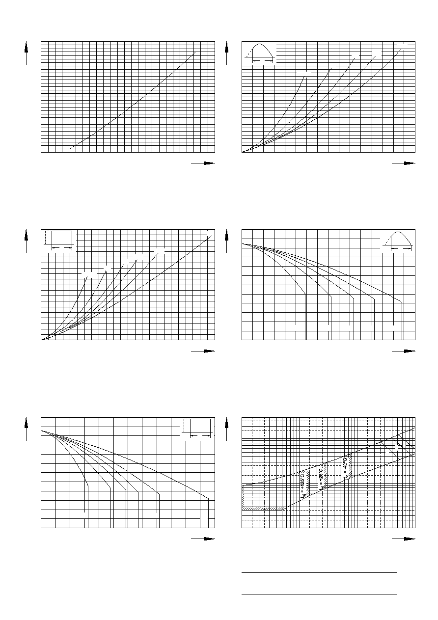
Bild / Fig. 1
Grenzdurchlaþkennlinie / Limiting on-state characteristic i
T
= f(v
T
)
t
vj
= t
vj max
Bild / Fig. 2
Durchlaþverlustleistung / On-state power loss P
TAV
= f(I
TAV
)
Parameter: Stromfluþwinkel / Current conduction angle
Bild / Fig. 3
Durchlaþverlustleistung / On-state power loss P
TAV
= f(I
TAV
)
Parameter: Stromfluþwinkel / Current conduction angle
Bild / Fig. 5
Hˆchstzul‰ssige Geh‰usetemperatur / Maximum allowable case temperature
t
c
= f(I
TAVM
)
Beidseitige K¸hlung / Two sided cooling
Parameter: Stromfluþwinkel / current conduction angle
Bild / Fig. 8
Hˆchstzul‰ssige Geh‰usetemperatur / Maximum allowable case temperature
t
c
= f(I
TAVM
)
Beidseitige K¸hlung / Two sided cooling
Parameter: Stromfluþwinkel / current conduction angle
Bild / Fig. 8
Steuercharakteristik mit Z¸ndbereichen / Gate characteristic with trigging
areas v
G
= f(i
G
), V
D
= 6 V
Parameter:
Steuerimpulsdauer / Puls duration t
g
Hˆchstzul‰ssige Spitzensteuerleistung
Maximum allowable peak gate power
a
b
c
[ms]
10
1
0,5
[W]
20
40
60
T 2709 N
T 2709 N / 2
P
TAV
[kW]
I
TAV
[kA]
180∞
120∞
90∞
60∞
= 30∞
8
7
6
5
4
3
2
1
0
3
2,5
2
1,5
1
0,5
0
4
3,5
T 2709 N / 3
P
TAV
[kW]
I
TAV
[kA]
180∞
120∞
90∞
60∞
= 30∞
10
8
6
4
2
00
0
1
2
3
4
5
6
DC
T 2709 N / 5
t
C
[∞C]
I
TAVM
[kA]
180∞
120∞
90∞
60∞
= 30∞
140
120
100
80
60
40
200
0,5
1
1,5
2
2,5
3
3,5
4
T 2709 N / 8
t
C
[∞C]
I
TAVM
[kA]
180∞
120∞
90∞
60∞
= 30∞
140
120
100
80
60
40
200
0
1
2
3
4
5
6
DC
T 2709 N / 8
v
G
[V]
i
G
[mA]
10
1
10
0
10
-1
10
1
10
2
10
3
10
4
2
3 4 5 6 7
2
3 4 5 6 7
2
3 4 5 6 7
2
3
4
5
7
2
3
4
5
7
2
3
a
b
c
T 2709 N / 1
16
14
12
10
8
6
4
2
0
i
T
[kA]
v
T
[V]
0,5
1
1,5
2
2,5
3
0
0

T 2709 N
Bild / Fig. 9
Z¸ndverzug / Gate controlled delay time t
gd
= f(i
GM
), t
vj
= 25∞C,
di
G
/dt = i
GM
/1µs
a - Maximaler Verlauf / Limiting characteristic
b - Typischer Verlauf / Typical characteristic
Bild / Fig. 10
Sperrverzˆgerungsladung / Recovered charge Q
r
= f(di/dt)
t
vj
= t
vj max
, v
R
0,5 V
RRM
, v
RM
= 0,8 V
RRM
Parameter: Durchlaþstrom / On-state current i
TM
Bild / Fig. 11
Transienter innerer W‰rmewiderstand / Transient thermal impedance
Z
thJC
= f(t)
Beidseitige K¸hlung / Two-sided cooling
Parameter: Stromfluþwinkel / Current conduction angle
Bild / Fig. 12
Transienter innerer W‰rmewiderstand / Transient thermal impedance
Z
thJC
= f(t)
Beidseitige K¸hlung / Two-sided cooling
Parameter: Stromfluþwinkel / Current conduction angle
Analytische Elemente des transienten W‰rmewiderstandes Z
thJC
pro Zweig f¸r DC
Analytical elements of transient thermal impedance Z
thJC
per arm for DC
Pos. n
R
thn
[∞C/W]
n
[s]
Beidseitige K¸hlung / Two-sided cooling
1
2
3
4
5
6
Analytische Funktion / Analytical function:
n
max
n=1
Z
thJC
= R
thn
(1-e )
t
-
n
0,00003
0,00039
0,00123
0,0028
0,00338
0,000055 0,00392
0,0152
0,2068
1,0914
T 2709 N / 9
t
gd
[µs]
i
GM
[mA]
10
-1
10
1
10
2
10
3
10
4
2
3 4 5 6 7
2
3 4 5 6 7
2
3 4 5 6 7
a
10
0
10
1
10
2
10
3
2
3
5
2
3
5
2
3
5
2
3
5
b
T 2709 N / 10
Q
r
[µAs]
-di/dt [A/µs]
10
0
10
1
10
2
2
3
4 5 6 7
2
3
4 5 6 7
10
4
10
3
2
3
4
5
6
8
2
4000 A
i
TM
=
100 A
200 A
2000 A
1000 A
500 A
T 2709 N / 11
Z
thJC
[∞C/W]
t [s]
0,010
0,008
0,006
0,004
0,002
0
10
-2
10
-1
10
0
10
1
10
2
10
-3
2 3 4 6
2 3 4 6
2 3 4 6
2 3 4 6
2 3 4 6
60∞
= 30∞
90∞
120∞
180∞
T 2709 N / 12
Z
thJC
[∞C/W]
t [s]
0,012
0,010
0,008
0,006
0,004
0,002
0
10
-2
10
-1
10
0
10
1
10
2
10
-3
2 3 4 6
2 3 4 6
2 3 4 6
2 3 4 6
2 3 4 6
DC
0
= 30∞
60∞
90∞
120∞
180∞
0
