T 568 N
Elektrische Eigenschaften
Electrical properties
Hˆchstzul‰ssige Werte
Maximum rated values
Periodische Vorw‰rts- und R¸ckw‰rts-
Spitzensperrspannung
repetitive peak forward off-state and
reverse voltages
t
vj
= -40∞C...t
vj max
V
DRM
, V
RRM
200 400 600
V
Vorw‰rts-Stoþspitzensperrspannung
non-repetitive peak forward off-state
voltage
t
vj
= -40∞C...t
vj max
V
DSM
= V
DRM
200 400 600
V
R¸ckw‰rts-Stoþspitzensperrspannung
non-repetitive peak reverse voltage
t
vj
= +25∞C...t
vj max
V
RSM
= V
RRM
250 450 650
V
Durchlaþstrom-Grenzeffektivwert
RMS on-state current
I
TRMSM
900
A
Dauergrenzstrom
average on-state current
t
c
= 85∞C
I
TAVM
568
A
Stoþstrom-Grenzwert
surge current
t
vj
= 25∞C, t
p
= 10 ms
I
TSM
7800
A
t
vj
= t
vj max
, t
p
= 10 ms
6700
A
Grenzlastintegral
I
2
t-value
t
vj
= 25∞C, t
p
= 10 ms
I
2
t
304000
A
2
s
t
vj
= t
vj max
, t
p
= 10 ms
225000
A
2
s
Kritische Stromsteilheit
critical rate of rise of on-state current
DIN IEC 747-6, f = 50 Hz,v
L
=10V,
(di
T
/dt)
cr
200
A/µs
i
GM
= 0,6 A, di
G
/dt = 0,6 A/µs
Kritische Spannungssteilheit
critical rate of rise of off-state voltage
t
vj
= t
vj max
, v
D
= 0,67 V
DRM
(dv
D
/dt)
cr
1000
V/µs
5.Kennbuchstabe/5th letter F
Charakteristische Werte
Characteristic values
Durchlaþspannung
on-state voltage
t
vj
= t
vj max
, i
T
= 2000 A
v
T
max. 1,76
V
Schleusenspannung
threshold voltage
t
vj
= t
vj max
V
T(TO)
0,8
V
Ersatzwiderstand
slope resistance
t
vj
= t
vj max
r
T
0,44
m
Z¸ndstrom
gate trigger current
t
vj
= 25 ∞C, v
D
= 6 V
I
GT
max. 150
mA
Z¸ndspannung
gate trigger voltage
t
vj
= 25 ∞C, v
D
= 6 V
V
GT
max. 1,4
V
Nicht z¸ndender Steuerstrom
gate non-trigger current
t
vj
= t
vj max
, v
D
= 6 V
I
GD
max. 5
mA
t
vj
= t
vj max
, v
D
= 0,5 V
DRM
max. 2,5
mA
Nicht z¸ndende Steuerspannung
gate non-trigger voltage
t
vj
= t
vj max
, v
D
= 0,5 V
DRM
V
GD
max. 0,2
V
Haltestrom
holding current
t
vj
= 25 ∞C, v
D
= 6 V, R
A
= 5
I
H
max. 200
mA
Einraststrom
latching current
t
vj
= 25 ∞C,v
D
= 6 V, R
GK
>
10
I
L
max. 600
A
i
GM
= 0,6 A, di
G
/dt = 0,6 A/µs, t
g
=20 µs
Vorw‰rts- und R¸ckw‰rts-Sperrstrom
forward off-state and reverse currents
t
vj
= t
vj max,
v
D
= V
DRM
, v
R
= V
RRM
i
D
, i
R
max. 40
mA
Z¸ndverzug
gate controlled delay time
DIN IEC 747-6 t
vj
=25∞C, i
GM
= 0,6 A,
di
G
/dt =0,6 A/µs
t
gd
max. 3,0
µs
Freiwerdezeit
circuit commutated turn-off time
t
vj
=t
vj max
, i
TM
=i
TAVM
, v
RM
=100V, v
DM
=0,67
V
DRM
, dv
D
/dt=20V/µs, -
di
T
/dt=10A/µs
t
q
typ. 200
µs
4.Kennbuchstabe/4th letter O
Thermische Eigenschaften
Thermal properties
Innerer W‰rmewiderstand, beidseitig
thermal resistance, junction to case for
two-sided cooling
=180∞ el, sin
R
thJC
max. 0,068
∞C/W
DC
max. 0,065
∞C/W
f¸r anodenseitige K¸hlung
for anode-sided cooling
=180∞ el, sin
R
thJC(A)
max. 0,113
∞C/W
DC
max. 0,110
∞C/W
f¸r kathodenseitige K¸hlung
for cathode-sided cooling
=180∞ el, sin
R
thJC(K)
max. 0,159
∞C/W
DC
max. 0,156
∞C/W
Ðbergangs-W‰rmewiderstand
thermal resistance, case to heatsink
beidseitig/two-sided
R
thCK
max. 0,015
∞C/W
einseitig/one-sided
max. 0,030
∞C/W
Hˆchstzul.Sperrschichttemperatur
max. junction temperature
t
vj max
140
∞C
Betriebstemperatur
operating temperature
t
c op
-40...+140
∞C
Lagertemperatur
storage temperature
t
stg
-40...+140
∞C
Mechanische Eigenschaften Mechanical properties
Si-Elemente mit Druckkontakt, Amplifying-
Gate
Si-pellet with pressure contact,amplifying
gate
Anpreþkraft
clamping force
F
4...8
kN
Gewicht
weight
G
typ. 70
g
Kriechstrecke
creepage distance
17
mm
Feuchteklasse
humidity classification
DIN 40040
C
Schwingfestigkeit
vibration resistance
f = 50 Hz
50
m/s≤
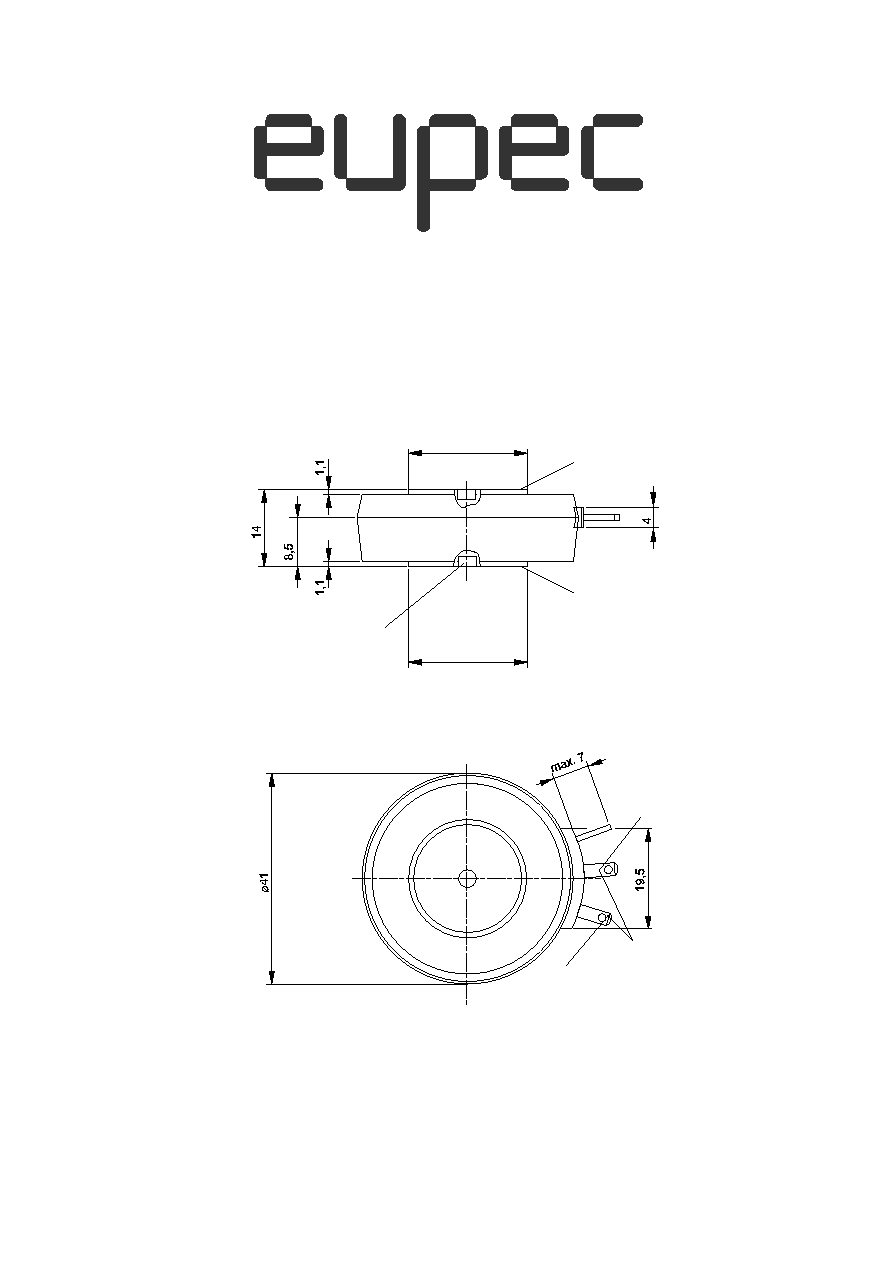
Maþbild, anliegend
outline, attached

2500
2000
1500
1000
500
0
0,6
v
T
[V]
i
T
[A]
T 568 N
Bild / Fig. 1
Grenzdurchlaþkennlinie / Limiting on-state characteristic
i
T
= f(v
T
), t
vj
= 140∞C
T 568 N / 1
Analytische Elemente des transienten W‰rmewiderstandes Z
thJC
pro Zweig f¸r DC
Analytical elements of transient thermal impedance Z
thJC
per arm for DC
Analytische Funktion / Analytical function:
n
max
n=1
Z
thJC
= R
thn
(1-e )
t
-
n
Pos. n
R
thn
[∞C/W]
n
[s]
Kathodenseitig / Cathode-sided
Pos. n
R
thn
[∞C/W]
n
[s]
Anodenseitig / Anode-sided
Pos. n
R
thn
[∞C/W]
n
[s]
Beidseitig / Two-sided
1
2
3
4
5
1
2
3
4
5
0,00832
0,0151
0,0181
0,0207
0,002856
0,000826
0,0166
0,0808
0,359
1,957
0,0098
0,0186
0,0157
0,0617
0,0502
0,00106
0,0227
0,0994
2,04
10,2
0,8
1
1,2
1,4
1,6
1,8
2
1
2
3
4
5
6
0,00961
0,00543
0,0209
0,0142
0,0271
0,0328
0,00104
0,0133
0,0364
0,23
1,52
10,5