 | –≠–ª–µ–∫—Ç—Ä–æ–Ω–Ω—ã–π –∫–æ–º–ø–æ–Ω–µ–Ω—Ç: MP3274SG | –°–∫–∞—á–∞—Ç—å:  PDF PDF  ZIP ZIP |

MP3274
1
Rev. 4.00
Fault Protected 32 Channel, 12-Bit
Data Acquisition Subsystem
FEATURES
∑
Complete 32-Channel 12-Bit A/D Converter
with Sample & Hold, Reference, Clock and
3-State Outputs
∑
Fast Conversion, less than 15
µ
S
∑
Microprocessor Bus Interface
∑
Parallel or Serial Data Output Modes
∑
65 ns Bus Access Time
∑
Remote Analog Ground Sensing
∑
Overvoltage Protected Input (
50 V over the
Supply Voltages)
∑
Precision Reference for Long Term Stability and
Low Gain T.C.
∑
Guaranteed Linearity Over Temperature
∑
Guaranteed Performance at +12/≠5 V,
±
12 &
±
15 V
∑
Low Power (3 mW per Channel Typical)
∑
16 Channel Version: MP3276 & MP3275
GENERAL DESCRIPTION
The MP3274 is a complete 32-channel, 12-bit Data Acquisi-
tion Subsystem with 3-state output buffers for direct interfacing
to 16-bit microprocessor buses. Implemented using an ad-
vanced BiCMOS process, the converter combines a 32-channel
passive overvoltage protected multiplexer instrumentation amp,
a sample & hold, a SAR, a 12-bit decoded D/A, a comparator, a
precision reference and the control logic to achieve an accurate,
repeated conversion in less than 15
µ
s, and a mux/instrumenta-
tion amp settling period of less than 10
µ
s.
A unique input design provides input overvoltage protection
to
50 V over the supply voltages. Therefore, an overvoltage
condition can exist on unselected channels without disrupting
the measured channel or operation of the MP3274! The internal
4 V reference has sufficient output current to provide other sys-
tem reference needs. Precision thin film scaling and offset resis-
tors are laser trimmed to provide for less than 2 LSB INL for +10
V inputs on all channels.
In addition, the MP3274 will output either full scale (0111 ....)
for overrange and ≠ full scale (1000....) for underrange condi-
tions. This greatly simplifies microprocessor software develop-
ment.
SIMPLIFIED BLOCK DIAGRAM
≠
+
Comp
SAR
4 V
REF
32
5
32 Ch.
MUX
AB0-4
(5 pins)
AIN0-31
(32 pins)
REF OUT
Control
Logic
GND REF.
DGND V
EE
VDAC
Latch/
Shift Register
3-State
Drivers
12
DB0-DB11
REF IN /2
12
V
DD
V
CC
CLK
WR RD
CS
PXS
ADEN
STL
STS
AGND
V
REF
AGND
2
AGND
3
AGND
REF IN

MP3274
2
Rev. 4.00
ORDERING INFORMATION
Package
Type
Temperature
Range
Part No.
DNL
(LSB)
PGA
≠40 to +85
∞
C
2
MP3274AG
INL
(LSB)
2
PGA
≠55 to +125
∞
C
MP3274SG*
2
2
PLCC
≠40 to +85
∞
C
2
MP3274AP
2
*Contact factory for non-compliant military processing
PIN CONFIGURATIONS
68 Pin PGA
G68
See the following
page for pin
numbers and
descriptions
and page 11 for
package dimensions
and connection table
Index
Mark
1
68 Pin PLCC
P68
See the following
page for pin
numbers and
descriptions

MP3274
3
Rev. 4.00
PIN OUT DEFINITIONS
61
1
V
EE
Negative Analog Supply
62
2
A
IN
24
Analog Input 24
63
3
A
IN
25
Analog Input 25
64
4
A
IN
26
Analog Input 26
65
5
A
IN
27
Analog Input 27
66
6
A
IN
28
Analog Input 28
67
7
A
IN
29
Analog Input 29
68
8
A
IN
30
Analog Input 30
1
9
A
IN
31
Analog Input 31
2
10
GND Ref.
Input Ground Reference
3
11
AGND
ADC Analog Ground
4
12
Ref In
Reference Input
5
13
Ref Out
Reference Output
6
14
AGND3
Reference Analog Ground
7
15
DGND
Digital Ground
8
16
DB0/SDC
Data Output Bit 0/Serial
Data Clock
9
17
N/C
No Connection
10
18
DB1
Data Output Bit 1
11
19
DB2
Data Output Bit 2
12
20
DB3
Data Output Bit 3
13
21
DB4
Data Output Bit 4
14
22
DB5
Data Output Bit 5
15
23
DB6
Data Output Bit 6
16
24
DB7
Data Output Bit 7
17
25
DB8
Data Output Bit 8
18
26
DB9
Data Output Bit 9
19
27
DB10
Data Output Bit 10
20
28
DB11/SDO
Data Output Bit 11/Serial
Data Out
21
29
STS
Conversion Status
22
30
STL
Mux Settling Status
23
31
PXS
Parallel/XSerial
24
32
RD
Read Enable
25
33
CS
Chip Select
26
34
WR
Write Enable
NAME
DESCRIPTION
27
35
ADEN
Address Enable
28
36
AB4
Channel Address 4
29
37
AB3
Channel Address 3
30
38
AB2
Channel Address 2
31
39
AB1
Channel Address 1
32
40
AB0
Channel Address 0
33
41
V
DD
Positive Digital Supply
34
42
V
CC
Positive Analog Supply
35
43
A
IN
0
Analog Input 0
36
44
A
IN
1
Analog Input 1
37
45
A
IN
2
Analog Input 2
38
46
A
IN
3
Analog Input 3
39
47
A
IN
4
Analog Input 4
40
48
A
IN
5
Analog Input 5
41
49
A
IN
6
Analog Input 6
42
50
A
IN
7
Analog Input 7
43
51
N/C
No Connection
44
52
A
IN
8
Analog Input 8
45
53
A
IN
9
Analog Input 9
46
54
A
IN
10
Analog Input 10
47
55
A
IN
11
Analog Input 11
48
56
A
IN
12
Analog Input 12
49
57
A
IN
13
Analog Input 13
50
58
A
IN
14
Analog Input 14
51
59
A
IN
15
Analog Input 15
52
60
AGND2
Analog Ground Mux Return
53
61
A
IN
16
Analog Input 16
54
62
A
IN
17
Analog Input 17
55
63
A
IN
18
Analog Input 18
56
64
A
IN
19
Analog Input 19
57
65
A
IN
20
Analog Input 20
58
66
A
IN
21
Analog Input 21
59
67
A
IN
22
Analog Input 22
60
68
A
IN
23
Analog Input 23
DESCRIPTION
PLCC
PIN NO.
PGA
PADS
NAME
PLCC
PIN NO.
PGA
PADS

MP3274
4
Rev. 4.00
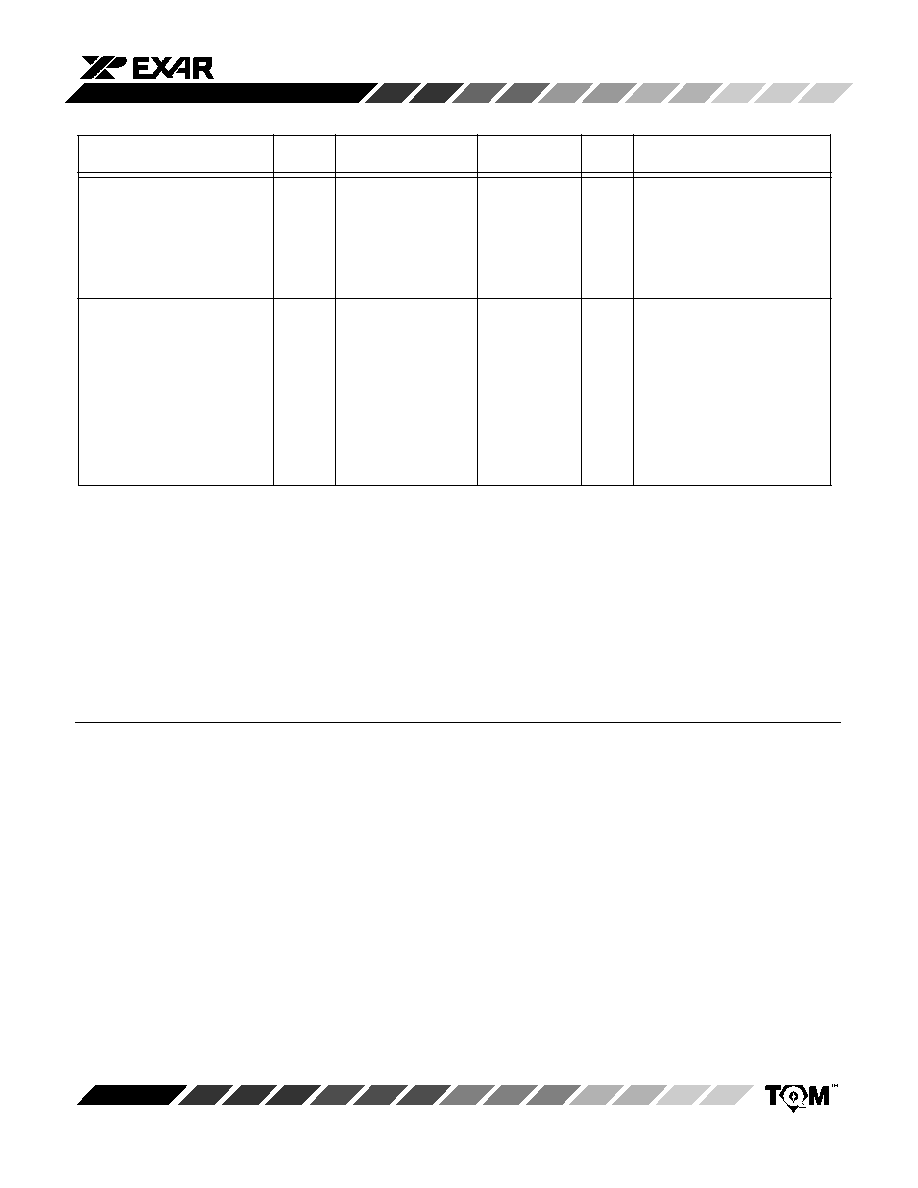
ELECTRICAL CHARACTERISTICS TABLE
Unless Otherwise Specified: V
DD
= 5 V, V
CC
= 15 V, V
EE
= ≠15 V, GNDRef = 0 V, T
A
= 25
∞
C,
V
REF
IN = Ref Out
25
∞
C
Parameter
Symbol
Min
Typ
Max
Min
Max
Units
Test Conditions/Comments
Resolution (All Grades)
N
12
12
Bits
KEY FEATURES
Resolution
12
12
Bits
Conversion Time, Per Channel
t
CONVR
15
15
µ
s
ACCURACY (A, S Grade)
1
Differential Non-Linearity
DNL
3/4
2
2
LSB
Integral Non-Linearity
INL
1
2
2
LSB
Best Fit Line
(Max INL ≠ Min INL)/2
Zero Code Error
EZS
2
5
10
LSB
fff to 000 [hex] transition
Full Scale Error
EFS
0.1
0.35
0.5
%
V
REF
IN = 4.000 V
POWER SUPPLY REJECTION
Max change in Full Scale
Calibration
V
CC
= 15 V
1.5 V or 12 V
0.6 V
1
1
LSB
V
DD
= 5 V
0.25 V
2
2.5
LSB
V
EE
= ≠15 V
1.5 V or
≠12 V
0.6 V or
1
1
LSB
≠5 V
0.25 V
REFERENCE VOLTAGES
Ref. Voltage Input
Ref In
3.6
4.4
V
R
IN
]
5K
; V
DD
= 5 V
Ref. Voltage Output
Ref Out
3.975
4.025
Ref. Source Current
3.0
4.0
3.0
mA
Ref. Sink Current
20
µ
A
ANALOG INPUT
2
Input Voltage Range
5
V
IN
≠10
10
≠10
10
V
Ground Reference
GND Ref.
CM Range
≠3
3
≠3
3
V
CM RR
TBD
LSB/V
Input Resistance
R
IN
100
130
100
k
Input Capacitance
C
IN
5
pF
Aperture Delay
t
AP
180
ns
From WR low to high after STL
high to low
Channel-to-Channel Isolation
2
≠80
≠70
dB
DC
DIGITAL INPUTS
CS, WR, RD AB0-AB4,
ADEN
Logical "1" Voltage
V
IH
2.4
5.5
2.4
5.5
V
Logical "0" Voltage
V
IL
≠0.5
0.8
≠0.5
0.8
V
Leakage Currents
6
I
IN
≠5
5
≠10
10
µ
A
V
IN
=GND to V
DD
Input Capacitance
2
5
pF
Tmin to Tmax
MP3274
5
Rev. 4.00
ELECTRICAL CHARACTERISTICS TABLE (CONT'D)
Description
Symbol
Min
Typ
Max
Min
Max
Units
Conditions
DIGITAL OUTPUTS
C
OUT
=15 pF
(Data Format 2's Complement)
DB0/SDC≠DB11/SDO, STS, STL
Logical "1" Voltage
V
OH
4.0
2.4
V
I
SOURCE
= 0.5 mA
Logical "0" Voltage
V
OL
0.4
0.4
V
I
SINK
= 1.6 mA
Tristate Leakage
I
OZ
≠5
5
≠5
5
µ
A
V
OUT
=GND to V
DD
POWER SUPPLIES
Operating Range
V
DD
+4.5
+5.5
+4.5
+5.5
V
V
CC
+11.4
+16.5
+11.4
+16.5
V
V
EE
≠4.75
≠16.5
≠4.75
≠16.5
V
Tested at ≠11.4 and ≠16.5 only
Operating Current
I
DD
2
7
7
mA
I
CC
5
8
8
mA
I
EE
1.5
3
3
mA
Power Dissipation
110
200
200
mW
25
∞
C
Tmin to Tmax
NOTES
1
Tester measures code transitions by dithering the voltage of the analog input (V
IN
). The difference between the measured and the
ideal code width is the DNL error. The INL error is the maximum distance (in LSBs) from the best fit line to any transition voltage
2
Guaranteed. Not tested.
3
Specified values guarantee functionality. Refer to other parameters for accuracy.
4
Input bandwidth is a measure of performance of the A/D input stage (S/H + amplifier). Refer to other parameters for accuracy
within the specified bandwidth.
5
All channel input pins and ground reference pin have protection which becomes active above
60 V.
6
All digital inputs have diodes to V
DD
and AGND. Input DC currents will not exceed specified limits for any input voltage between GND
and V
DD
.
Specifications are subject to change without notice
ABSOLUTE MAXIMUM RATINGS
(T
A
= +25
∞
C unless otherwise noted)
1, 2
V
CC
to DGND
0 to +16.5 V
. . . . . . . . . . . . . . . . . . . . . . . . . . . .
V
EE
to DGND
0 to ≠16.5 V
. . . . . . . . . . . . . . . . . . . . . . . . . . . .
V
DD
to DGND
0 to +7 V
. . . . . . . . . . . . . . . . . . . . . . . . . . . . . . .
AGND to DGND
±
1 V
. . . . . . . . . . . . . . . . . . . . . . . . . . . . . . . . .
Digital Inputs/Outputs
to DGND
≠0.5 V to V
LOGIC
+0.5 V
. . . . . . . . . . . . . . . . . . . . .
Analog Inputs (A
IN
0 ≠ A
IN
31, GND REF)
to AGND
±
60 V
. . . . . . . . . . . . . . . . . . . . . . . . . . . . . . . . . . . . .
REF OUT
Indefinite short to DGND,
. . . . . . . . . . . . . . . . . . .
Momentary short to V
CC
Maximum Junction Temperature
150
∞
C
. . . . . . . . . . . . . . . . .
Package Power Dissipation Rating to 75
∞
C
PGA, PLCC
1800 mW
. . . . . . . . . . . . . . . . . . . . . . . . . . . .
Derates above 75
∞
C
25 mW/
∞
C
. . . . . . . . . . . . . . . . . . . . .
Lead Temperature, Soldering
300
∞
C, 10 Sec
. . . . . . . . . . . .
Storage Temperature (Ceramic)
≠65
∞
C to +150
∞
C
. . . . . . . .
NOTES:
1
Stresses above those listed under "Absolute Maximum Ratings" may cause permanent damage to the device. This is a
stress rating only and functional operation at or above this specification is not implied. Exposure to maximum rating
conditions for extended periods may affect device reliability.
2
Any input pin which can see a value outside the absolute maximum ratings
should be protected by Schottky diode clamps
(HP5082-2835) from input pin to the supplies.
All logic inputs have protection diodes which will protect the device from
short transients outside the supplies of less than 100mA for less than 100
µ
s.