 | –≠–ª–µ–∫—Ç—Ä–æ–Ω–Ω—ã–π –∫–æ–º–ø–æ–Ω–µ–Ω—Ç: MP3275AE | –°–∫–∞—á–∞—Ç—å:  PDF PDF  ZIP ZIP |

MP3275
1
Rev. 4.00
Fault Protected 16 Channel, 12-Bit
Data Acquisition Subsystem
FEATURES
∑
Fault Protected 16-Channel 12-Bit A/D
Converter with Sample & Hold, Reference,
Clock and 3-State Outputs
∑
Fast Conversion, less than 15
µ
S
∑
2's Complement and Serial Data Output
∑
Remote Analog Ground Sensing
∑
Overvoltage Protected Input (
50 V over the
Supply Voltages)
∑
Precision Reference for Long Term Stability and
Low Gain T.C.
∑
Guaranteed Linearity Over Temperature
∑
Guaranteed Performance at +12/≠5 V,
±
12 &
±
15 V
∑
Low Power (7 mW per Channel Typical)
∑
Parallel Version: MP3276
∑
32 Channel Version: MP3274
GENERAL DESCRIPTION
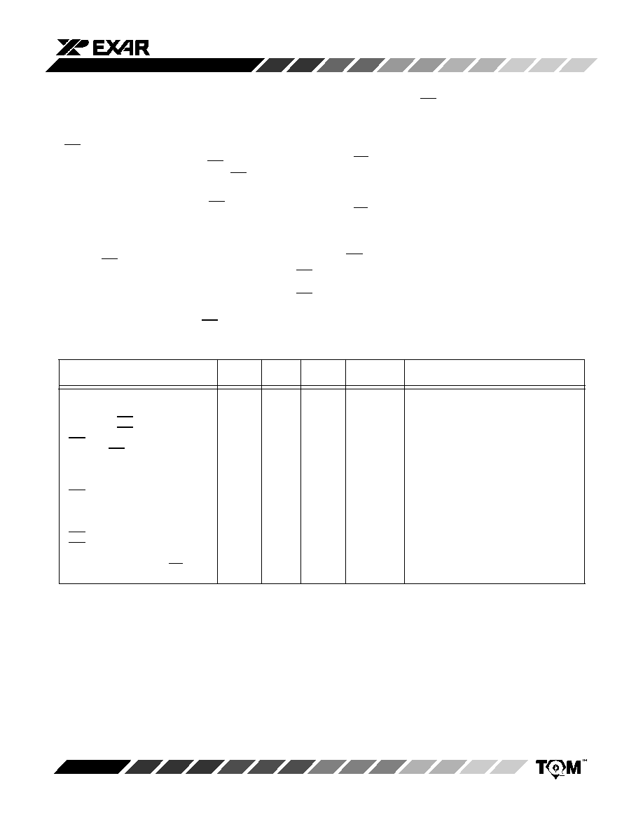
The MP3275 is a complete 16-channel, 12-bit Data Acquisi-
tion Subsystem with serial data port. Implemented using an ad-
vanced BiCMOS process, the converter combines a 16-channel
passive overvoltage-protected multiplexer instrumentation
amp, a sample & hold, a SAR, a 12-bit decoded D/A, a compa-
rator, a precision reference and the control logic to achieve an
accurate conversion in less than 15
µ
s, and a mux/instrumenta-
tion amp settling period of less than 10
µ
s.
A unique input design provides input overvoltage protection
to
50 V over the supply voltages. The circuit design can allow
for an overvoltage condition on unselected channels without dis-
rupting the measured channel or operation of the MP3275! The
internal 4 V reference has sufficient output current to provide
other system reference needs. Precision thin film scaling and
offset resistors are laser trimmed to provide for less than 2 LSB
INL for +10 V inputs on all channels.
In addition, the MP3275 will output either full scale (0111 ....)
for overrange and ≠ full scale (1000....) for underrange condi-
tions. This greatly simplifies microprocessor software develop-
ment.
SIMPLIFIED BLOCK DIAGRAM
≠
+
Comp
SAR
4 V
REF
16
4
16
Ch.
MUX
AB0-3
(4 pins)
A
IN0
-15
(16 pins)
REF OUT
Control
Logic
GND REF.
DGND V
EE
VDAC
Latch/
Shift Register
3-State
Driver
12
SDO
REF IN /2
12
V
DD
V
CC
CLK
WR
RD
SDC
ADEN
STL
STS
V
REF
AGND
2
AGND
3
AGND
DGND
CS

MP3275
2
Rev. 4.00
ORDERING INFORMATION
Package
Type
Temperature
Range
Part No.
DNL
(LSB)
PQFP
≠40 to +85
∞
C
2
MP3275AE
INL
(LSB)
2
PIN CONFIGURATIONS
44 Pin PQFP
Q44
See the following
page for pin
numbers and
descriptions
33
23
22
12
1
11
34
44
Index

MP3275
3
Rev. 4.00
PIN OUT DEFINITIONS
1
V
EE
≠ Analog Supply. ≠4.75 To ≠ 16.5
2
A
IN
12
Channel 12 Analog Input, 1100
3
A
IN
13
Channel 13 Analog Input, 1101
4
A
IN
14
Channel 14 Analog Input, 1110
5
A
IN
15
Channel 15 Analog Input, 1111
6
GNDREF
+ Input To Mux / Instrumentation Amp
7
AGND
A/D Section Analog Ground
8
REF
Reference Output
9
AGND
3
Reference Analog Ground
10
DGND
Digital Logic And Output Ground
11
SDC
Serial Data Clock
12
N/C
No Connection
13
N/C
No Connection
14
N/C
No Connection
15
N/C
No Connection
16
SDO
Serial Data Out
17
STS
Conversion Status, Converting=1
18
STL
Input Settling Period State = 1
19
DGND
Digital Gnd, Low Current
20
RD
Enable Serial Data Out
21
CS
Chip Select
22
WR
Input Address And Conversion Control
PIN NO.
NAME
DESCRIPTION
PIN NO.
23
ADEN
Address Update Enable=1, Ignore=0
24
AB3
Input Address Bit 3, (MSB)
25
AB2
Input Address Bit 2
26
AB1
Input Address Bit 1
27
AB0
Input Address Bit 0, (LSB)
28
V
DD
Digital Logic & Output Supply, +4.75 to
+ 5.25 Volts
29
V
CC
Analog + Supply, +11.4 to + 16.5 Volts
30
A
IN
0
Channel 0 Analog Input, 0000
31
A
IN
1
Channel 1 Analog Input, 0001
32
A
IN
2
Channel 2 Analog Input, 0010
33
A
IN
3
Channel 3 Analog Input, 0011
34
N/C
No Connection
35
A
IN
4
Channel 4 Analog Input, 0100
36
A
IN
5
Channel 5 Analog Input, 0101
37
A
IN
6
Channel 6 Analog Input, 0110
38
A
IN
7
Channel 7 Analog Input, 0111
39
AGND
2
Agnd For Input Mux Section
40
A
IN
8
Channel 7 Analog Input, 1000
41
N/C
No Connection
42
A
IN
9
Channel 9 Analog Input, 1001
43
A
IN
10
Channel 10 Analog Input, 1010
44
A
IN
11
Channel 11 Analog Input, 1011
NAME
DESCRIPTION

MP3275
4
Rev. 4.00
ELECTRICAL CHARACTERISTICS TABLE
Unless Otherwise Specified: V
DD
= 5 V, V
CC
= 15 V, V
EE
= ≠15 V, GNDRef = 0 V, T
A
= 25
∞
C
25
∞
C
Parameter
Symbol
Min
Typ
Max
Min
Max
Units
Test Conditions/Comments
Resolution (All Grades)
N
12
12
Bits
KEY FEATURES
Resolution
12
12
Bits
Conversion Time, Per Channel
t
CONVR
15
15
µ
s
ACCURACY (A Grade)
1
Refer to
Table 6. for
output coding
Differential Non-Linearity
DNL
3/4
2
2
LSB
Integral Non-Linearity
INL
1
2
2
LSB
Best Fit Line
(Max INL ≠ Min INL)/2
Zero Code Error
EZS
2
5
10
LSB
fff to 000 [hex] transition
Full Scale Error
EFS
0.1
0.35
0.5
%
V
REF
IN = 4.000 V
POWER SUPPLY REJECTION
Max change in Full Scale
Calibration
V
CC
= 15 V
1.5 V or 12 V
0.6 V
1
1
LSB
V
DD
= 5 V
0.25 V
2
2.5
LSB
V
EE
= ≠15 V
1.5 V or
≠12 V
0.6 V
1
1
LSB
≠5 V
0.25 V
REFERENCE VOLTAGES
Voltage Output
V
REF(+)
3.975
4.0
4.025
3.970
4.030
V
Ref. Source Current
3.0
4.0
3.0
mA
Ref. Sink Current
20
µ
A
ANALOG INPUT
Input Voltage Range
3
V
IN
≠10
10
≠10
10
V
Ground Reference
GND Ref.
CM Range
2
≠3
+3
≠3
3
V
CM RR
TBD
LSB/V
Input Resistance
R
IN
100
130
100
k
Input Capacitance
2
C
IN
5
pF
Aperture Delay
2
t
AP
180
ns
From WR low to high after STL
high to low
Channel-to-Channel Isolation
2
≠80
≠70
dB
DC
DIGITAL INPUTS
WR, RD AB0-AB4,
ADEN, SDC
Logical "1" Voltage
V
IH
2.4
5.5
2.4
5.5
V
Logical "0" Voltage
V
IL
≠0.5
0.8
≠0.5
0.8
V
Leakage Currents
4
I
IN
≠5
5
≠10
10
µ
A
V
IN
=GND to V
DD
Input Capacitance
2
5
pF
Tmin to Tmax

MP3275
5
Rev. 4.00
ELECTRICAL CHARACTERISTICS TABLE (CONT'D)
Description
Symbol
Min
Typ
Max
Min
Max
Units
Conditions
DIGITAL OUTPUTS
C
OUT
=15 pF
(Data Format 2's Complement)
SDO, STS, STL
Logical "1" Voltage
V
OH
4.0
2.4
V
I
SOURCE
= 0.5 mA
Logical "0" Voltage
V
OL
0.4
0.4
V
I
SINK
= 1.6 mA
Tristate Leakage
I
OZ
≠5
5
≠5
5
µ
A
V
OUT
=GND to V
DD
POWER SUPPLIES
Operating Range
V
DD
+4.5
+5.5
+4.5
+5.5
V
V
CC
+11.4
+16.5
+11.4
+16.5
V
V
EE
≠4.75
≠16.5
≠4.75
≠16.5
V
Tested at ≠11.4 and ≠16.5 only
Operating Current
I
DD
2
7
7
mA
I
CC
5
8
8
mA
I
EE
1.5
3
3
mA
Power Dissipation
110
200
200
mW
25
∞
C
Tmin to Tmax
NOTES
1
Tester measures code transitions by dithering the voltage of the analog input (V
IN
). The difference between the measured and the
ideal code width is the DNL error. The INL error is the maximum distance (in LSB's) from the best fit line to any transition voltage
2
Guaranteed. Not tested.
3
All channel input pins and ground reference pin have protection which becomes active above
60 V.
4
All digital inputs have diodes to V
DD
and AGND. Input DC currents will not exceed specified limits for any input voltage between
AGND and V
DD
.
Specifications are subject to change without notice
ABSOLUTE MAXIMUM RATINGS (T
A
= +25
∞
C unless otherwise noted)
1, 2
V
CC
to AGND
0 to +16.5 V
. . . . . . . . . . . . . . . . . . . . . . . . . . . .
V
EE
to AGND
0 to ≠16.5 V
. . . . . . . . . . . . . . . . . . . . . . . . . . . .
V
DD
to AGND
0 to +7 V
. . . . . . . . . . . . . . . . . . . . . . . . . . . . . . .
AGND to DGND
±
1 V
. . . . . . . . . . . . . . . . . . . . . . . . . . . . . . . . .
Digital Inputs or Outputs (WR, RD, CS, AB0-AB4, ADEN,
SDC) to DGND
≠0.5 V to V
DD
+0.5 V
. . . . . . . . . . . . . . . . . .
Analog Inputs (A
IN
0 ≠ A
IN
15, GND REF)
to AGND
±
60 V
. . . . . . . . . . . . . . . . . . . . . . . . . . . . . . . . . . . . . .
REF OUT
Indefinite short to DGND,
. . . . . . . . . . . . . . . . . . .
Momentary short to V
CC
Maximum Junction Temperature
150
∞
C
. . . . . . . . . . . . . . . . .
Package Power Dissipation Rating to 75
∞
C
PQFP
750 mW
. . . . . . . . . . . . . . . . . . . . . . . . . . . . . . . . . .
Derates above 75
∞
C
10 mW/
∞
C
. . . . . . . . . . . . . . . . . . . . .
Lead Temperature, Soldering
300
∞
C, 10 Sec
. . . . . . . . . . . .
Storage Temperature (Ceramic)
≠65
∞
C to +150
∞
C
. . . . . . . .
NOTES:
1
Stresses above those listed under "Absolute Maximum Ratings" may cause permanent damage to the device. This is a
stress rating only and functional operation at or above this specification is not implied. Exposure to maximum rating
conditions for extended periods may affect device reliability.
2
Any input pin which can see a value outside the absolute maximum ratings
should be protected by Schottky diode clamps
(HP5082-2835) from input pin to the supplies.
All logic inputs have protection diodes which will protect the device from
short transients outside the supplies of less than 100mA for less than 100
µ
s.

MP3275
6
Rev. 4.00
PRODUCT INFORMATION
Basic Description
The MP3275 is a fault protected data acquisition subsystem
available in monolithic form. This product contains all of the cir-
cuitry necessary to acquire 16 channels of quasi differential or
single-ended analog signals at
10 V input range and 15kHz
bandwidth. Connections to power, the analog input signals and
the digital system are all that is required. The MP3275's input
circuitry is protected against active input signals present with the
MP3275 power off. This is also the case for any channel exceed-
ing the MP3275 analog input dynamic range without interfering
with the channel being digitized. The channel address and
channel conversion can be managed in two ways: random
channel conversion or same channel conversion. Circuitry on
the chip adds a MUX/instrumentation amp settling delay of 10
µ
s
max, when a new channel is selected (ADEN = 1). Conversion
start is initiated without delay for the single-channel case (ADEN
= 0). Data is available in serial format.
TIMING
Control and Timing Considerations
The MP3275 can be operated in the stand-alone mode, with
one line for control and everything else hard-wired; or under mi-
croprocessor control, where changes can be made dynamically.
There are 4 control lines: ADEN, WR, CS and RD with their
functions described in
Table 1.
Note 1: If RD = 1, SDO remain high impedance. It is recommended that RD will not change during a conversion in
order to reduce noise. It is further recommended that RD = 1 during conversion to reject any noise present on the
SDO.
Table 1. Logic Truth Table
CS
WR
RD
ADEN
Data
STL
STS
Comments
1
X
X
X
≠≠
0
0
No operation
0
1
0
Hi-Z
0
0
No operation if ADEN = 0
0
1
1
Hi-Z
0
Input MUX channel selected, STL set on WR falling edge
0
0
1
X
Hi-Z
1
0
MUX select disabled
0
1
X
Hi-Z
0
Start convert on WR rising edge
0
1
1
X
Hi-Z
Start convert on STL falling edge
0
1
1
X
Hi-Z
0
STS goes low at end of conversion
0
1
X
≠≠
0
0
SDO enabled
0
X
0
X
ADC
0
0
Data from previous conversion on SDO
0
X
X
Hi-Z
0
0
SDO disabled
0
1
X
X
Hi-Z
0
1
SDO/RD disabled while STS high
0
X
0
X
Last ADC
1
0
Data from last conversion on SDO
0
0
0
Hi-Z
0
STL, MUX select disabled with ADEN = 0,
SDO disabled on STS rising edge
0
0
X
ADC
0
New data appears on SDO on falling edge of STS
Read ADC Data
(See Figure 2. and Table 3.)
ADC Channel Select and Start Convert
(See Figure 1. and Table 2.)
MP3275
7
Rev. 4.00
The MP3275 is easily interfaced to a wide variety of digital
systems. Discussion of the timing requirements of the MP3275
control signals follows.
Figure 1. shows a complete timing diagram for the MP3275
convert start operation.
WR is used to initiate a conversion.
A conversion is started by taking WR low, then high again
(conversion is enabled on the rising edge of WR). There are two
possible conditions that will affect conversion timing.
1. ADEN = 1. At the falling edge of WR, the input channel is
determined by the data present on the address bits. The
track and hold begins to settle after which STL returns low,
indicating that the multiplexer, buffer amp, and sample/hold
have settled to less than 1/2 LSB of final value. If the rising
edge of WR returns high prior to STL going low, conversion
will begin on the falling edge of STL. If the rising edge of WR
is delayed until after STL returns low, the input signal is sam-
pled and the conversion is started at the rising edge of WR
giving the user better control of the sampling time.
2. ADEN = 0. At the falling edge of WR the data present at the
address is ignored and the channel selected during the pre-
vious conversion remains selected. In this case the track
and hold settling time is omitted and STL never goes high. At
the rising edge of WR the input signal is sampled, and con-
version is started.
There are two possible states that the data output could be in
during a conversion.
1. If RD is held high during a conversion the output would re-
main high impedance throughout the conversion. This is the
preferred method of operation as any noise present on SDO
is rejected.
2. If RD is held low during a conversion, the data present SDO
will be from the previous conversion until the present conver-
sion is completed, when STS returns low. The data from the
new conversion will be available through SDO. The state of
RD should not change during a conversion.
Once a conversion is started and the STL or STS line goes
high, convert start commands will be ignored until the conver-
sion cycle is completed. The SDO output buffer cannot be en-
abled during conversion. In addition, all input and output
changes during conversion can introduce noise, and should be
avoided when possible.
ADC Control Timing
Table 2. ADC Write Timing
(See Figure 1.)
25
∞
C
Tmin to
Tmax
Limits
Comments/Test Conditions
Address to WR Set-Up Time
t
3
0
0
ns min
Address to WR Hold Time
t
4
0
0
ns min
WR Pulse Width
t
5
80
80
ns min
ADEN to WR Set-Up Time
t
6
0
ns min
ADC Conversion Timing
WR to STL
Delay
t
7
150
150
ns max
Load ckt of Figure 5, C
L
= 20 pF,
ADEN = 1
STL High (Settling Period)
t
8
10
15
µ
s max
Load ckt of Figure 5, C
L
= 20 pF
STL to STS Low (Converting)
t
9
15
20
µ
s max
Load ckt of Figure 5, C
L
= 20 pF
WR to STS High (ADEN = 0)
t
12
200
250
ns max
STL = 0 when ADEN = 0
WR to STS Low (ADEN = 1)
t
10
15
20
µ
s max
STS High to SDO Relinquish Time
t
13
150
150
ns max
Load ckt of Figure 4
STS Low to Data Valid (RD = 0)
t
14
50
50
ns max
Load ckt of Figure 3, C
L
= 20 pF
ADC Write Timing
Time
Interval

MP3275
8
Rev. 4.00
WR
ADDRESS
Figure 1. Timing for ADC Channel Select Start Conversion
STL
ADEN
STS
SDO
RD = 0
SDO
RD = 1
HIGH Z
Previous ADC Data
New ADC Data
t
3
t
4
t
5
t
6
t
7
t
8
t
9
t
11
10
t
t
12
t
14
t
13
Table 3. ADC Read Timing
(
See Figure 2.)
25
∞
C
Tmin to
Tmax
Limits
Comments/Test Conditions
RD to Data Valid Delay
t
17
100
150
ns max
Load ckt of
Figure 3., C
L
= 20 pF
150
200
ns max
Load ckt of
Figure 3., C
L
= 100 pF
SDO Relinquish Time after
t
18
100
150
ns max
Load ckt of
Figure 4.
RD High
RD Pulse Width
t
19
100
150
ns min
ADC Read Timing
Time
Interval
RD
DATA
Figure 2. Timing for ADC Read
t
18
t
Valid
17

MP3275
9
Rev. 4.00
Figure 3. Load Circuit for Data
Access Time Test
3k
C
L
a. High-Z to V
ON
DB
N
3k
b. High-Z to V
OL
+5 V
Figure 4. Load Circuit for
Bus Relinquish Time Test
3k
10pF
a. V
ON
to High-Z
3k
10pF
b. V
OL
to High-Z
+5 V
N
DB
N
DB
N
DB
C
L
C
L
Figure 5. Load Circuit for WR to STS Delay
DGND
STL, STS
Serial Data Output
The serial data output sequence is MSB (DB11) first to LSB
(DB0) last. The MSB (DB11) data bit appears at SDO when STS
goes low. The second most significant bit appears at SDO on
the SDC high-to-low transition next. The LSB (DB0) is present
at SDO on the 11th SDC high-to-low transition.
Further information regarding serial control and timing is
shown in
Figure 6., Table 4. and Table 5.
For a minimum interconnect serial environment, the channel
address state can be generated in at least two ways, using an
address counter, or using an address serial to parallel converter.
WR can then be used as the counter clock or shift register load
signal as well as the A/D converter start convert signal on the ris-
ing edge. (Note that the falling edge loads the address present at
the address port.)
SDC
SDO
Figure 6. Serial Data Mode Timing
DB11 (MSB)
DB10
t
21
t
22
SDC should be in a high state during the STS high period. SDC can make the first high to low transition after t
21
.
t
20
STS
See Table 4
«««««
«««««

MP3275
10
Rev. 4.00
Table 4. Serial Data Output Mode Timing
(
See Figure 6.)
25
∞
C
Tmin to
Tmax
Limits
Comments/Test Conditions
STS low to SDO Valid,
t
20
50
50
ns max
Load Ckt 4 of
Figure 3.
RD = 0
Minimum clock high pulse width
t
21
50
80
ns max
SDC low to data valid delay
t
22
150
200
ns max
Load ckt of
Figure 3., C
L
= 20pF
200
250
ns max
Load ckt of
Figure 3., C
L
= 100pF
Serial Data Output Timing
Time
Interval
Note 1: If RD = 1, data outputs remain high impedance. It is recommended that RD will not change during a con-
version in order to reduce noise. It is further recommended that RD = 1 during conversion to reject any noise
present on the data bus.
Table 5. Logic Truth Table ≠ Serial Data Output
WR
RD
ADEN
Data
STL
STS
Comments
1
0
Hi-Z
0
0
X
No operation if ADEN = 0
1
1
Hi-Z
0
X
Input MUX channel selected, STL
set on falling edge of WR
0
1
X
Hi-Z
1
0
X
MUX select disabled
1
X
Hi-Z
0
X
Start convert on WR rising edge
1
1
X
Hi-Z
X
Start convert on STL falling edge
1
1
X
Hi-Z
0
X
STS goes low at end of conversion
ADC Channel Select and Start Convert
DB0/SDC
1
X
≠≠
0
0
1
Serial output (SDO) and
serial clock input (SDC) enabled
X
X
X
MSB (DB11)
0
0
1
MSB data available at SDO
X
0
X
DB10
0
0
Next significant bit shifted out to SDO
X
0
X
DB10
0
0
0
No Operation
X
0
X
DB10
0
0
No Operation
X
0
X
DB9
0
0
Next significant bit shifted out to SDO
X
X
Hi-Z
0
0
X
Data outputs/SDC input disabled
1
X
X
Hi-Z
0
1
X
Data outputs/RD disabled when STS = 1
0
0
Hi-Z
0
1
STL, MUX select disabled when ADEN = 0
0
X
MSB (DB11)
0
1
New data appears at SDO on falling
edge of STS
Read ADC Data (
See Figure 6. and Table 4.)
Table 6. Key Output Codes vs. Input Voltage (2's Complement Code)
2's Complement Output Code (Hexidecimal)
Ideal Transition Voltage
+FS ≠ 1 1/2 LSB
0 V +1/2 LSB
0 V ≠1/2 LSB
≠FS +1/2 LSB
0111
0000
1111
1000
1111
0000
1111
0000
1110 (7fe) to
0000 (000) to
1111 (fff) to
0000(800) to
0111
0000
0000
1000
1111
0000
0000
0000
1111 (7ff)
0001 (001)
0000 (000)
0001 (801)
MP3275
11
Rev. 4.00
APPLICATION INFORMATION
The MP3275 is a complete A/D converter system, with its
own built-in reference and clock. It may be used by itself ("stand-
alone" operation), or it may be interfaced with a microprocessor.
Successful application of the MP3275 requires careful atten-
tion to four main areas:
1)
Physical layout.
2)
Connection/Trimming according to mode of operation.
3)
Conditioning of input signals.
4)
Control and Timing considerations.
Physical Layout
The 12-bit accuracy of the MP3275 represents a dynamic
range of 72dB. Precautions must be taken to avoid any interfer-
ing signals, whether conducted or radiated, to assure that this is
not degraded.
∑
Avoid placing the chip and its analog signals near logic
traces. In general, using a double sided printed circuit
card with a good ground plane on the component side is
recommended. Routing analog signals between ground
traces will help isolate digital control logic. If these lines
cross, do so at right angles. The GND Ref. is the positive
terminal of the MUX/Instrumentation amplifier and will
provide common mode noise rejection. It should be
close to and shielded together with the channel inputs in
order to take advantage of this feature.
∑
Power supplies should be quiet and well regulated.
Grounds should be tied together at the package and
back to the system ground with a single path. Bypass the
supplies at the device with a 0.01 to 0.1
µ
F ceramic cap
and a 10-47
µ
F tantalum type, in parallel.
"Stand-Alone" Operation
The MP3275 can be used in "stand-alone" operation, which is
useful in systems not requiring full computer bus interface capa-
bility.
For this operation, CS = 0, ADEN = 1, and conversion is con-
trolled by WR. The 3-state buffer SDO is enabled when RD goes
low. There are two possible conditions that the 3-state buffer
could be in during a conversion. If RD goes low prior to WR the
output buffer is enabled and the data from the previous conver-
sion is available at the outputs during STL = 1. At the end of the
present conversion which is initiated at the rising edge of WR,
STS returns low and the new conversion result is placed on the
output data buffer.
If WR goes low prior to RD, the data buffer remains in a high
impedance state and conversion is initiated at the rising edge of
WR. Upon the end of the conversion the STS returns low and
the conversion result is placed on the output data buffers.
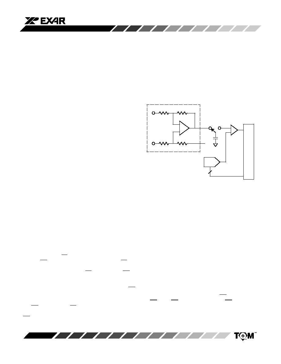
Ground Reference
The ground reference pin can be used for remote ground
sensing of a common mode input signal with a maximum 6 V p-p
around AGND.
This common input can also be used to dither each input's
"zero". By averaging multiple conversions digitally, higher reso-
lution for each input conversion can be obtained. Patterns for
this dither can be a ramp, a stair step, or white noise.
COMP
S
A
R
VDAC
12
130k
26k
130k
26k
1 of 16
GND Ref.
Figure 7. Equivalent Input Circuit
1/2
V
REF
Quasi Differential Sampling
Method 1
For remote ground sensing where the remote ground does
not change more than
3 V from the A/D ground, connect GND
Ref to the remote ground.
Method 2
Where Method 1 applies to each channel or group of chan-
nels, add a mux to allow connecting the appropriate ground to
GND Ref.
Method 3
Use two parts. Tie both GND Ref pins together and connect
this node to the "common" remote GND. Control the sample
point by connecting each STL through an "OR" gate whose out-
put is "NAND" connect with WR (inverted WR). Use this output
as WR to both WR inputs. By controlling the WR, sample delay
differences between the two converters is minimized. Two parts
from the same date code will further minimize this difference.
Treat one A/D as the (+) terminal and the other as the (≠) termi-
nal of the differential signal. Now the difference can be taken
digitally.

MP3275
12
Rev. 4.00
A
≠≠
3.15
≠≠
0.124
A
1
0.25
≠≠
0.01
≠≠
A
2
2.6
2.8
0.102
0.110
B
0.3
0.4
0.012
0.016
C
0.13
0.23
0.005
0.009
D
16.95
17.45
0.667
0.687
D
1
13.9
14.1
0.547
0.555
e
1.00 BSC
0.039 BSC
L
0.65
1.03
0.026
0.040
0
∞
7
∞
0
∞
7
∞
Coplanarity = 4 mil max.
44 LEAD PLASTIC QUAD FLAT PACK
(14mm x 14mm PQFP, METRIC)
Q44
SYMBOL
MIN
MAX
MIN
MAX
INCHES
MILLIMETERS
33
23
22
12
1
11
34
44
D
D
1
D
D
1
B
e
L
A
2
C
A
1
A

MP3275
13
Rev. 4.00
Notes

MP3275
14
Rev. 4.00
Notes

MP3275
15
Rev. 4.00
Notes

MP3275
16
Rev. 4.00
NOTICE
EXAR Corporation reserves the right to make changes to the products contained in this publication in order to im-
prove design, performance or reliability. EXAR Corporation assumes no responsibility for the use of any circuits de-
scribed herein, conveys no license under any patent or other right, and makes no representation that the circuits are
free of patent infringement. Charts and schedules contains here in are only for illustration purposes and may vary
depending upon a user's specific application. While the information in this publication has been carefully checked;
no responsibility, however, is assumed for inaccuracies.
EXAR Corporation does not recommend the use of any of its products in life support applications where the failure or
malfunction of the product can reasonably be expected to cause failure of the life support system or to significantly
affect its safety or effectiveness. Products are not authorized for use in such applications unless EXAR Corporation
receives, in writing, assurances to its satisfaction that: (a) the risk of injury or damage has been minimized; (b) the
user assumes all such risks; (c) potential liability of EXAR Corporation is adequately protected under the circum-
stances.
Copyright EXAR Corporation
Datasheet April 1995
Reproduction, in part or whole, without the prior written consent of EXAR Corporation is prohibited.