 | –≠–ª–µ–∫—Ç—Ä–æ–Ω–Ω—ã–π –∫–æ–º–ø–æ–Ω–µ–Ω—Ç: MP7528LS | –°–∫–∞—á–∞—Ç—å:  PDF PDF  ZIP ZIP |
MP7528
1
Rev. 2.00
FEATURES
∑
On-Chip Latches for Both DACs
∑
+5 V to +15 V Operation
∑
DACs Matched to 1%
∑
Four Quadrant Multiplication
∑
15 V CMOS Compatible
∑
See MP7529A or MP7529B for Improved Performance
CMOS
Dual Buffered Multiplying 8-Bit
Digital-to-Analog Converter
APPLICATIONS
∑
Microprocessor Controlled Gain Circuits
∑
Microprocessor Controlled Attenuator Circuits
∑
Microprocessor Controlled Function Generation
∑
Precision AGC Circuits
∑
Bus Structured Instruments
GENERAL DESCRIPTION
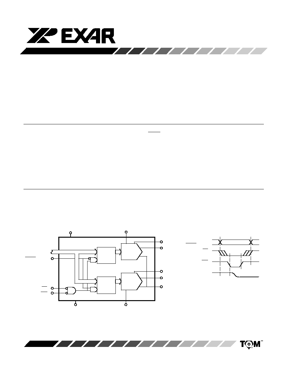
The MP7528 is a dual 8-bit digital/analog converter designed
using EXAR's proven decoded DAC architecture. It features ex-
cellent DAC-to-DAC matching and guaranteed monotonicity.
Separate on-chip latches are provided for each DAC to allow
easy microprocessor interface.
Data is transferred into either of the two DAC data latches via
a common 8-bit TTL/CMOS compatible input port. Control input
DACA/DACB determines which DAC is to be loaded. The
MP7528's load cycle is similar to the write cycle of a random ac-
cess memory and the device is bus compatible with most 8-bit
microprocessors.
The device operates from a +5V to +15V power supply with
only 2 mA of current (maximum).
Both DACs offer excellent four quadrant multiplication char-
acteristics with a separate reference input and feedback resistor
for each DAC.
SIMPLIFIED BLOCK AND TIMING DIAGRAM
DGND
LATCH A
LATCH B
DAC A
DAC B
D
E
Q
D
E
Q
DB7-DB0
OUT
DB7-DB0
AGND
V
DD
V
REFA
R
FBA
I
OUTA
R
FBB
I
OUTB
V
REFB
DACA/DACB
CS
WR
DACA/DACB
CS
WR
MP7528
2
Rev. 2.00
Ceramic Dip
MP7528AD
Ceramic Dip
MP7528BD
Ceramic Dip
MP7528CD
Ceramic Dip
MP7528SD*
Ceramic Dip
MP7528TD*
≠40 to +85
∞
C
≠40 to +85
∞
C
≠40 to +85
∞
C
≠55 to +125
∞
C
≠55 to +125
∞
C
+1
+1/2
+1/4
+1
+1/2
+6
+4
+3
+6
+4
+1
+1
+1
+1
+1
ORDERING INFORMATION
Package
Type
Temperature
Range
Part No.
Plastic Dip
MP7528JN
Plastic Dip
MP7528KN
Plastic Dip
MP7528LN
PLCC
MP7528JP
PLCC
MP7528KP
PLCC
MP7528LP
SOIC
MP7528JS
SOIC
MP7528KS
SOIC
MP7528LS
+1
+1/2
+1/4
+1
+1/2
+1/4
+1
+1/2
+1/4
+3
≠40 to +85
∞
C
≠40 to +85
∞
C
≠40 to +85
∞
C
≠40 to +85
∞
C
≠40 to +85
∞
C
≠40 to +85
∞
C
≠40 to +85
∞
C
≠40 to +85
∞
C
≠40 to +85
∞
C
+6
+4
+3
+6
+4
+3
+6
+4
+1
+1
+1
+1
+1
+1
+1
+1
+1
INL
(LSB)
Gain Error
(LSB)
DNL
(LSB)
*Contact factory for non-compliant military processing
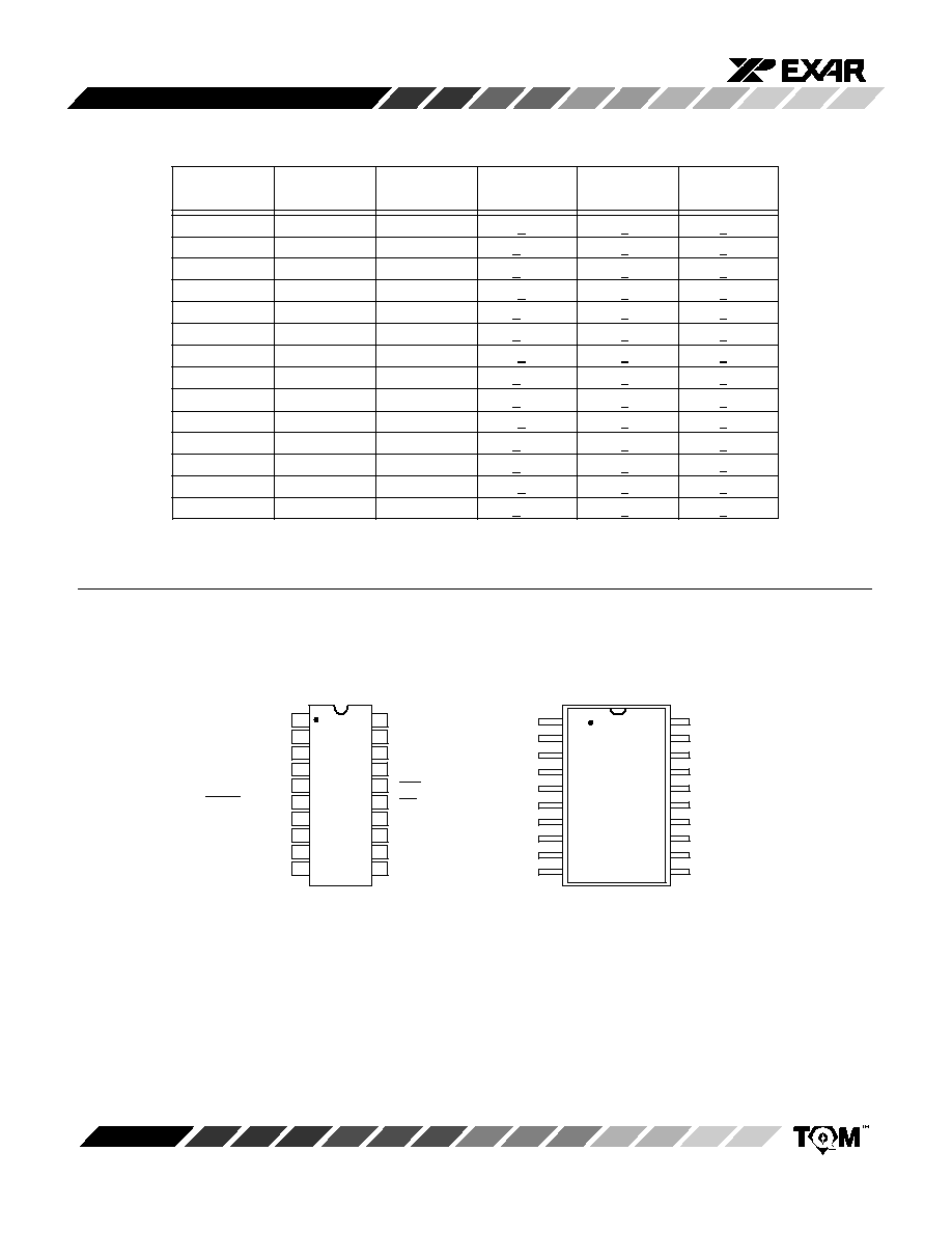
PIN CONFIGURATIONS
AGND
DGND
(MSB) DB7
DB6
DB5
DB4
DB0 (LSB)
DB1
DB2
DB3
1
2
3
4
5
6
7
8
9
10
20
19
18
17
16
15
14
13
12
11
20 Pin CDIP, PDIP (0.300")
D20, N20
R
FBA
V
REFA
R
FBB
V
REFB
V
DD
20 Pin SOIC (Jedec, 0.300")
S20
20
1
11
10
2
3
4
5
6
7
15
14
13
12
17
16
8
9
19
18
See
Pin Out
at Left
I
OUTB
I
OUTA
See Packaging Section for Package Dimensions
DACA/DACB
CS
WR

MP7528
3
Rev. 2.00
PIN CONFIGURATIONS (CONT'D)
3
2
1
20
19
9
10
11
12
13
4
5
6
7
8
18
17
16
15
14
20 Pin PLCC
P20
AGND
R
FBA
DGND
(MSB) DB7
DB6
V
REFA
DB5
DB4
DB3
DB2
DB1
DB0
V
REFB
V
DD
R
FBB
(LSB)
I
OUTB
I
OUTA
DACA/DACB
CS
WR
PIN OUT DEFINITIONS
1
AGND
Analog Ground
2
I
OUTA
Current Out DAC A
3
R
FBA
Feedback Resistor for DAC A
4
V
REFA
Reference Input for DAC A
5
DGND
Digital Ground
6
DAC A/
DAC Select
DAC B
7
DB7 (MSB)
Data Input Bit 7
8
DB6
Data Input Bit 6
9
DB5
Data Input Bit 5
10
DB4
Data Input Bit 4
11
DB3
Data Input Bit 3
12
DB2
Data Input Bit 2
13
DB1
Data Input Bit 1
14
DB0 (LSB)
Data Input Bit 0
15
CS
Chip Select
16
WR
Write
17
V
DD
Power Supply
18
V
REFB
Reference Input for DAC B
19
R
FBB
Feedback Resistor for DAC B
20
I
OUTB
Current Out DAC B
PIN NO.
NAME
DESCRIPTION

MP7528
4
Rev. 2.00
ELECTRICAL CHARACTERISTICS
(V
DD
= + 5 V, V
REF
= +10 V unless otherwise noted)
25
∞
C
Tmin to Tmax
Parameter
Symbol
Min
Typ
Max
Min
Max
Units
Test Conditions/Comments
STATIC PERFORMANCE
1
Resolution (All Grades)
N
8
8
Bits
Integral Non-Linearity
INL
LSB
End Point Linearity Spec.
(Relative Accuracy)
J, A, S
+1
+1
K, B, T
+1/2
+1/2
L, C
+1/4
+1/4
Monotonicity
Guaranteed over temp
Differential Non-Linearity
DNL
+1
+1
LSB
All grades monotonic over full
J, A, S
temperature range.
K, B, T
L, C
Gain Error
GE
LSB
Using Internal R
FB
J, A, S
+4
+6
Digital Inputs = V
INH
K, B, T
+2
+4
L, C
+1
+3
Gain Temperature Coefficient
2
TC
GE
+70
ppm/
∞
C
Gain/
Temperature
Power Supply Rejection Ratio
PSRR
+200
+400
ppm/%
|
Gain/
V
DD
|
V
DD
= + 5%
Digital Inputs = V
INH
Output Leakage Current (Pin 2)
I
OUT1
+50nA
+400nA
nA
Digital Inputs = V
INL
Output Leakage Current (Pin 20)
I
OUT2
+50nA
+400nA
nA
Digital Inputs = V
INH
Input Resistance
V
REFA
8
15
8
15
k
TC = ≠300 ppm/
∞
C max.
V
REFB
8
15
8
15
k
11 k
typical
Input Resistance Matching
+1
+1
%
DYNAMIC PERFORMANCE
2
R
L
=100
, C
L
=13pF
Harmonic Distortion
THD
≠85
dB
V
IN
= 6V
RMS
@ 1 KHz
Digital Crosstalk
Q
30
nVs
Measured for code transition
Z
S
to F
SS
Channel-to-Channel Isolation
CCI
≠77
dB
AC Feedthrough at I
OUT1
F
T
≠70
≠65
dB
V
REF
= 10kHz, 20 Vp-p, sinewave
Glitch Energy
Egl
160
nVs
Z
S
to F
S
Input Change
Propagation Delay
t
PD
220
270
ns
From digital input to 90%
of final analog output current

MP7528
5
Rev. 2.00
ELECTRICAL CHARACTERISTICS (CONT'D)
25
∞
C
Tmin to Tmax
Parameter
Symbol
Min
Typ
Max
Min
Max
Units
Test Conditions/Comments
DIGITAL INPUTS
3
Logical "1" Voltage
V
IH
2.4
2.4
V
Logical "0" Voltage
V
IL
0.8
0.8
V
Input Leakage Current
I
LKG
+1
+10
µ
A
Input Capacitance
2
Data C
IN
10
10
pF
Control
C
IN
15
15
pF
ANALOG OUTPUTS
2
Output Capacitance
C
OUTA
120
120
pF
DAC Inputs all 1's
C
OUTA
50
50
pF
DAC Inputs all 0's
C
OUTB
120
120
pF
DAC Inputs all 1's
C
OUTB
50
50
pF
DAC Inputs all 0's
POWER SUPPLY
5
Functional Voltage Range
2
V
DD
4.5
15.75
4.5
15.75
V
Supply Current
I
DD
2
2
mA
All digital inputs = 0 V or all = 5 V
2
2
mA
All digital inputs = V
IL
or all = V
IH
SWITCHING
CHARACTERISTICS
4
Chip Select to Write Set-Up Time
t
CS
200
230
ns
Chip Select to Write Hold Time
t
CH
20
30
ns
DAC Select to Write Set-Up Time
t
AS
200
230
ns
DAC Select to Write Hold Time
t
AH
20
30
Data Valid to Write Set-Up Time
t
DS
110
130
ns
Data Valid to Write Hold Time
t
DH
0
0
ns
Write Pulse Width
t
WR
180
200
ns
NOTES:
Specifications are subject to change without notice
1
Full Scale Range (FSR) is 10V for unipolar mode.
2
Guaranteed but not production tested.
3
Digital input levels should not go below ground or exceed the positive supply voltage, otherwise damage may occur.
4
See timing diagram.
5
Specified values guarantee functionality. Refer to other parameters for accuracy.