 | –≠–ª–µ–∫—Ç—Ä–æ–Ω–Ω—ã–π –∫–æ–º–ø–æ–Ω–µ–Ω—Ç: MP7541B | –°–∫–∞—á–∞—Ç—å:  PDF PDF  ZIP ZIP |
MP7541B
1
Rev. 2.00
FEATURES
∑
ESD Protection: 2000 V Minimum
∑
Full Four Quadrant Multiplication
∑
Low Glitch Energy
∑
12-Bit Linearity (End-Point)
∑
Guaranteed Monotonic. All Grades. All Temperatures.
∑
TTL/5 V CMOS Compatible
∑
Stable, More Accurate Segmented Architecture
≠
2.0 ppm/
∞
C Typ. Gain Error Tempco
≠
0.2 ppm/
∞
C Max. Linearity Tempco
≠
Lowest Sensitivity to Output Amplifier Offset
∑
Latch-Up Free
15 V CMOS
Multiplying 12-Bit
Digital-to-Analog Converter
APPLICATIONS
∑
Industrial Automation
∑
Automatic Test Equipment
∑
Disk Drive Servo Systems
∑
Digital/Synchro Conversion
∑
Programmable Gain Amplifiers
∑
Ratiometric A/D Conversion
∑
Function Generation
∑
Digitally Controlled Filters
GENERAL DESCRIPTION
The MP7541B is a pin-compatible replacement which offers
superior performance in latch-up and ESD protection versus the
comparable 7541 and 7541A. The high ESD protection will re-
duce failures caused by mishandling. These devices are manu-
factured using patented advanced thin film resistors on a double
metal CMOS process which result in ultra stable thin film and su-
perior long life reliability and stability. The MP7541B incorpo-
rates a bit decoding technique yielding lower glitch, higher
speed and excellent accuracy over temperature and time. The
MP7541B's outstanding features are:
Stability: Both Integral Non-Linearity (INL) and Differential-
Non-Linearity (DNL) are rated at 0.2 ppm/
∞
C maximum.
Monotonicity is guaranteed over the entire temperature range.
Gain Temperature Coefficient (TC
GE
) is 2.0 ppm/
∞
C typical.
Lower Sensitivity to Output Amplifier Offset: Multiplying
DACs provide an output current into a virtual ground of the out-
put op amp. Additional linearity error caused by the op amp is
reduced by a factor of 3 in the MP7541B versus conventional
R-2R DACs.
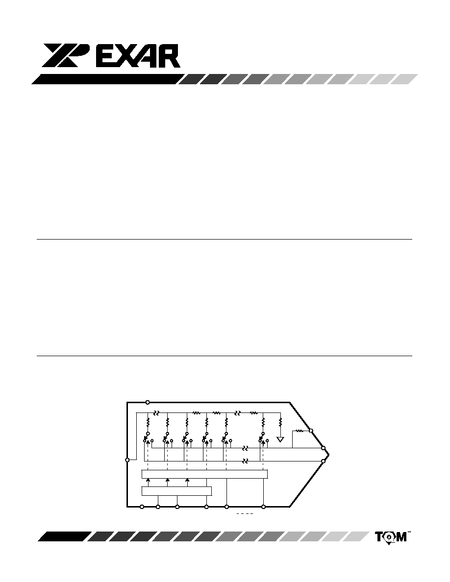
3-7 Decoder
80k
40k
Switch Drivers
40k
40k
GND BIT 1
BIT 2
BIT 3
BIT 4
BIT 12
(LSB)
(MSB)
10k
80k
"1"
"1"
"1"
"1"
"1"
SIMPLIFIED BLOCK DIAGRAM
"1"
V
DD
V
REF
R
FB
I
OUT1
I
OUT2

MP7541B
2
Rev. 2.00
ORDERING INFORMATION
Package
Type
Temperature
Range
Part No.
Ceramic Dip
MP7541BSD*
Ceramic Dip
MP7541BTD*
Plastic Dip
MP7541BJN
Plastic Dip
MP7541BKN
SOIC
MP7541BJS
SOIC
MP7541BKS
≠55 to +125
∞
C
≠40 to +85
∞
C
≠55 to +125
∞
C
≠40 to +85
∞
C
≠40 to +85
∞
C
≠40 to +85
∞
C
1
1
1
1/2
1/2
1/2
8
5
1
1
1
1/2
1/2
1/2
INL
(LSB)
Gain Error
(LSB)
DNL
(LSB)
8
5
5
8
*Contact factory for non-compliant military processing
PIN CONFIGURATIONS
GND
(MSB) BIT 1
BIT 2
BIT 3
BIT 4
BIT 5
BIT 6
BIT 12 (LSB)
BIT 11
BIT 10
BIT 9
BIT 8
BIT 7
18 Pin PDIP, CDIP (0.300")
N18, D18
1
2
3
4
5
6
7
8
9
18
17
16
15
14
13
12
11
10
R
FB
V
REF
V
DD
I
OUT1
I
OUT2
18
1
10
9
2
3
4
5
6
7
15
14
13
12
11
17
16
8
18 Pin SOIC (Jedec, 0.300")
S18
BIT 12 (LSB)
BIT 11
BIT 10
BIT 9
BIT 8
BIT 7
R
FB
V
REF
V
DD
GND
(MSB) BIT 1
BIT 2
BIT 3
BIT 4
BIT 5
BIT 6
I
OUT1
I
OUT2
See Packaging Section for Package Dimensions
PIN OUT DEFINITIONS
PIN NO.
NAME
DESCRIPTION
1
I
OUT1
Current Output 1
2
I
OUT2
Current Output 2
3
GND
Ground
4
BIT 1
Data Input Bit 1 (MSB)
5
BIT 2
Data Input Bit 2
6
BIT 3
Data Input Bit 3
7
BIT 4
Data Input Bit 4
8
BIT 5
Data Input Bit 5
9
BIT 6
Data Input Bit 6
PIN NO.
NAME
DESCRIPTION
10
BIT 7
Data Input Bit 7
11
BIT 8
Data Input Bit 8
12
BIT 9
Data Input Bit 9
13
BIT 10
Data Input Bit 10
14
BIT 11
Data Input Bit 11
15
BIT 12
Data Input Bit 12 (LSB)
16
V
DD
Positive Power Supply
17
V
REF
Reference Input Voltage
18
R
FB
Internal Feedback Resistor

MP7541B
3
Rev. 2.00
ELECTRICAL CHARACTERISTICS
V
DD
= + 15 V, V
REF
= +10 V, I
OUT1
= I
OUT2
= GND = 0 V Unless Otherwise Noted.
25
∞
C
Tmin to Tmax
Parameter
Symbol
Min
Typ
Max
Min
Max
Units
Test Conditions/Comments
STATIC PERFORMANCE
1
Resolution (All Grades)
N
12
12
Bits
Integral Non-Linearity
INL
LSB
End Point Linearity
(Relative Accuracy)
K, T
+1/2
+1/2
J, S
+1
+1
Differential Non-Linearity
DNL
LSB
All grades
K, T
+1/2
+1/2
monotonic over full
J, S
+1
+1
temperature range.
Gain Error
GE
LSB
Using Internal R
FB
K, T
+3
+5
J, S
+6
+8
Gain Temperature Coefficient
2
TC
GE
+2
ppm/
∞
C
Gain/
Temperature
Power Supply Rejection Ratio
PSRR
5
+50
+100
ppm/%
|
Gain/
V
DD
|
V
DD
= + 5%
Output Leakage Current
I
LKG
5
+10
+200
nA
Digital Inputs = 0 or 5 V
DYNAMIC PERFORMANCE
2
RL=100
, C
EXT
=13pF
Current Settling Time
t
S
0.65
1.0
µ
s
Full scale change
to 1/2 LSB
AC Feedthrough at I
OUT1
F
T
1.0
mV p-p
V
REF
= 20 V p-p
10kHz, Sinewave
Glitch Energy
Egl
500
nVs
00--0 to 11--1
Input Change
Propagation Delay
t
PD
60
ns
From 50% of digital
input to 10% of final
analog output
current
REFERENCE INPUT
Input Resistance
R
IN
5
10
20
5
20
k
DIGITAL INPUTS
Logical "1" Voltage
V
IH
3.0
2.4
3.0
V
Logical "0" Voltage
V
IL
0.8
0.8
V
Input Leakage Current
I
INH
, I
INL
+1.0
+1.0
µ
A
Input Capacitance
2
Data
C
IN
8.0
8.0
pF
ANALOG OUTPUTS
2
Output Capacitance
C
OUT1
100
pF
DAC all 1's
C
OUT1
50
pF
DAC all 0's
C
OUT2
50
pF
DAC all 1's
C
OUT2
100
pF
DAC all 0's
POWER SUPPLY
3
Functional Voltage Range
2
V
DD
4.5
16
4.5
16
V
Supply Current
I
DD
1.0
1.0
mA
All Digital Inputs = 0 or 5 V

MP7541B
4
Rev. 2.00
ELECTRICAL CHARACTERISTICS (CONT'D)
NOTES:
Specifications are subject to change without notice
1
Full Scale Range (FSR) is 10V for unipolar mode.
2
Guaranteed but not production tested.
3
Specified values guarantee functionality. Refer to other parameters for accuracy.
ABSOLUTE MAXIMUM RATINGS (T
A
= +25
∞
C unless otherwise noted)
1, 2
V
DD
to GND
0 to +17 V
. . . . . . . . . . . . . . . . . . . . . . . . . . . . . .
Digital Input Voltage to GND
GND ≠0.5 to V
DD
+0.5 V
. . . .
I
OUT1
, I
OUT2
to GND
GND ≠0.5 to V
DD
+0.5 V
. . . . . . . . . . .
V
REF
to GND
+25 V
. . . . . . . . . . . . . . . . . . . . . . . . . . . . . . . . . .
V
RFB
to GND
+25 V
. . . . . . . . . . . . . . . . . . . . . . . . . . . . . . . . . .
Storage Temperature
≠65
∞
C to +150
∞
C
. . . . . . . . . . . . . . . . .
Lead Temperature (Soldering, 10 seconds)
+300
∞
C
. . . . . .
Package Power Dissipation Rating to 75
∞
C
CDIP, PDIP, SOIC
850mW
. . . . . . . . . . . . . . . . . . . . . . . . .
Derates above 75
∞
C
11mW/
∞
C
. . . . . . . . . . . . . . . . . . . . .
NOTES:
1
Stresses above those listed under "Absolute Maximum Ratings" may cause permanent damage to the device. This is a
stress rating only and functional operation at or above this specification is not implied. Exposure to maximum rating
conditions for extended periods may affect device reliability.
2
Any input pin which can see a value outside the absolute maximum ratings
should be protected by Schottky diode clamps
(HP5082-2835) from input pin to the supplies.
All inputs have protection diodes which will protect the device from short
transients outside the supplies of less than 20mA for less than 100
µ
s.
APPLICATION NOTES
Refer to Section 8 for Applications Information
PERFORMANCE CHARACTERISTICS
Graph 1. Linearity Error vs.
Digital Input Code

MP7541B
5
Rev. 2.00
SYMBOL
MIN
MAX
MIN
MAX
A
0.097
0.104
2.464
2.641
A
1
0.0050
0.0115
0.127
0.292
B
0.014
0.019
0.356
0.483
C
0.0091
0.0125
0.231
0.318
D
0.451
0.461
11.46
11.71
E
0.292
0.299
7.42
7.59
e
0.050 BSC
1.27 BSC
H
0.400
0.410
10.16
10.41
h
0.010
0.016
0.254
0.406
L
0.016
0.035
0.406
0.889
0
∞
8
∞
0
∞
8
∞
INCHES
MILLIMETERS
18 LEAD SMALL OUTLINE
(300 MIL JEDEC SOIC)
S18
e
18
10
9
D
E
H
B
A
L
C
A
1
Seating
Plane
h x 45
∞