 | –≠–ª–µ–∫—Ç—Ä–æ–Ω–Ω—ã–π –∫–æ–º–ø–æ–Ω–µ–Ω—Ç: MP7614JN | –°–∫–∞—á–∞—Ç—å:  PDF PDF  ZIP ZIP |

MP7614
1
Rev. 2.00
FEATURES
∑
Full Four-Quadrant Multiplication
∑
Excellent Stability Over Temperature and Time
∑
Guaranteed Monotonic
∑
TTL/5 V CMOS Compatible
15 V CMOS
Multiplying 14-Bit
Digital-to-Analog Converter
∑
Low Sensitivity to Output Amplifier V
OS
∑
Low Glitch Energy
∑
16-Bit Version: MP7616
GENERAL DESCRIPTION
The MP7614 is a high density 14-bit CMOS multiplying Digi-
tal-to-Analog Converter. Silicon nitride passivation and un-
trimmed silicon chromium resistors have been combined to pro-
vide long term stability and reliability. Using the most significant
bit (MSB) segmentation technique, the MP7614 features 13-bit
(0.012%) differential and 12-bit (0.01%) integral linearity.
To achieve 13-bit linearity without laser trim, the MP7614 digi-
tally decodes the four MSB's into 15 equal current sources,
rather than the standard binary-weighted sources. Each resis-
tor contributes only 1/16 full scale output thus reducing the
matching accuracy requirement of the resistor and CMOS
switches from 0.0015% to 0.006%.
The decoding technique achieves an eightfold improvement
in differential linearity stability over temperature, an eightfold im-
provement in relative accuracy due to aging effects (long term
stability), a fourfold improvement in glitch amplitude, and a ten-
fold reduction in sensitivity to output amplifier offset voltage.
SIMPLIFIED BLOCK DIAGRAM
4 to 15 Decoder
R
R
R
R
R
R
R
R
R
R
R
R
R
R
R
10-Bit
DAC
1
(LSB)
To 10-Bit DAC
To Switches
V
DD
V
REF
I
OUT2
I
OUT1
R
FB
(MSB)
4
5
14
GND

MP7614
2
Rev. 2.00
ORDERING INFORMATION
Package
Type
Temperature
Range
Part No.
Ceramic Dip
MP7614KD
Ceramic Dip
MP7614TD*
Plastic Dip
MP7614JN
Plastic Dip
MP7614KN
≠40 to +85
∞
C
≠55 to +125
∞
C
+4
+2
+2
+2
+0.8
+0.8
+0.8
+0.8
+4
+2
+2
+2
≠40 to +85
∞
C
≠40 to +85
∞
C
SOIC
MP7614KS
+0.8
≠40 to +85
∞
C
+2
+2
INL
(LSB)
Gain Error
(% FSR)
DNL
(LSB)
*Contact factory for non-compliant military processing
PIN CONFIGURATIONS
GND
(MSB) BIT 1
BIT 2
BIT 3
BIT 4
BIT 5
BIT 6
BIT 7
BIT 14 (LSB)
BIT 13
BIT 12
BIT 11
BIT 10
BIT 9
BIT 8
20 Pin CDIP, PDIP (0.300")
D20, N20
1
2
3
4
5
6
7
8
9
10
20
19
18
17
16
15
14
13
12
11
I
OUT1
I
OUT2
R
FB
V
REF
V
DD
20
1
11
10
2
3
4
5
6
7
15
14
13
12
17
16
8
9
19
18
20 Pin SOIC (Jedec, 0.300")
S20
BIT 14 (LSB)
BIT 13
BIT 12
BIT 11
BIT 10
BIT 9
BIT 8
R
FB
V
REF
V
DD
GND
(MSB) BIT 1
BIT 2
BIT 3
BIT 4
BIT 5
BIT 6
BIT 7
I
OUT1
I
OUT2
See Packaging Section for Package Dimensions
1
I
OUT1
Current Output 1
2
I
OUT2
Current Output 2
3
GND
Ground
4
BIT 1
Data Input Bit 1 (MSB)
5
BIT 2
Data Input Bit 2
6
BIT 3
Data Input Bit 3
7
BIT 4
Data Input Bit 4
8
BIT 5
Data Input Bit 5
9
BIT 6
Data Input Bit 6
10
BIT 7
Data Input Bit 7
PIN OUT DEFINITIONS
PIN NO.
NAME
DESCRIPTION
11
BIT 8
Data Input Bit 8
12
BIT 9
Data Input Bit 9
13
BIT 10
Data Input Bit 10
14
BIT 11
Data Input Bit 11
15
BIT 12
Data Input Bit 12
16
BIT 13
Data Input Bit 13
17
BIT 14
Data Input Bit 14 (LSB)
18
V
DD
Positive Power Supply
19
V
REF
Reference Input Voltage
20
R
FB
Internal Feedback Resistor
PIN NO.
NAME
DESCRIPTION

MP7614
3
Rev. 2.00
ELECTRICAL CHARACTERISTICS
(V
DD
= + 15 V, V
REF
= +10 V unless otherwise noted)
25
∞
C
Tmin to Tmax
Parameter
Symbol
Min
Typ
Max
Min
Max
Units
Test Conditions/Comments
STATIC PERFORMANCE
1
FSR = Full Scale Range
Resolution (All Grades)
N
14
14
Bits
Integral Non-Linearity
5
INL
LSB
Best Fit Straight Line Spec.
(Relative Accuracy)
(Max INL ≠ Min INL) / 2
J, S
+4
+4
K, T
+2
+2
Differential Non-Linearity
5
DNL
LSB
J, S
+4
+4
K, T
+2
+2
Gain Error
GE
0.8
+0.8
% FSR
Using Internal R
FB
Gain Temperature Coefficient
2
TC
GE
+1.0
+2.0
ppm/
∞
C
Gain/
Temperature
Non-Linearity Tempco
2
+0.2
+0.5
ppm/
∞
C
Differential Linearity Tempco
2
+0.2
+0.5
ppm/
∞
C
Power Supply Rejection Ratio
PSRR
+5
+50
+50
ppm/%
|
Gain/
V
DD
|
V
DD
= + 5%
Output Leakage Current
6
I
OUT
+1
+10
+200
nA
DYNAMIC PERFORMANCE
2
Current Settling Time
t
S
2
µ
s
To 0.01% of FSR; all digital inputs
low to high and high to low
Feedthrough at I
OUT1
F
T
1
2
mV p-p
V
REF
= 20 V p-p @ 10 kHz
REFERENCE INPUT
Input Resistance
R
IN
1
3
10
1
10
k
DIGITAL INPUTS
3
Logical "1" Voltage
V
IH
3.0
2.4
3.0
V
Logical "0" Voltage
V
IL
0.8
0.8
V
Input Leakage Current
I
LKG
+1.0
+1.0
µ
A
ANALOG OUTPUTS
2
Output Capacitance
C
OUT1
100
pF
DAC Inputs all 1's
C
OUT1
50
pF
DAC Inputs all 0's
C
OUT2
50
pF
DAC Inputs all 1's
C
OUT2
100
pF
DAC Inputs all 0's
POWER SUPPLY
4
Functional Voltage Range
2
V
DD
4.5
15
16
4.5
16
V
Supply Current
I
DD
0.4
4
4
mA
All digital inputs = 0 V or all = 5 V

MP7614
4
Rev. 2.00
ELECTRICAL CHARACTERISTICS (CONT'D)
NOTES:
Specifications are subject to change without notice
1
Full Scale Range (FSR) is 10V for unipolar mode.
2
Guaranteed but not production tested.
3
Digital input levels should not go below ground or exceed the positive supply voltage, otherwise damage may occur.
4
Specified values guarantee functionality. Refer to other parameters for accuracy.
5
Linearity error is degraded by 65
µ
V for every mV of voltage offset at output amplifier.
6
Output leakage current refers to I
OUT1
. 1 LSB of current constantly flows into I
OUT2
(30nA at 5 k
input impedance, V
REF
= +10 V)
due to ladder termination into I
OUT2
.
ABSOLUTE MAXIMUM RATINGS (T
A
= +25
∞
C unless otherwise noted)
1, 2
V
DD
to GND
0 to +17 V
. . . . . . . . . . . . . . . . . . . . . . . . . . . . . .
Digital Input Voltage to GND
GND ≠0.5 to V
DD
+0.5 V
. . . .
I
OUT1
, I
OUT2
to GND
GND ≠0.5 to V
DD
+0.5 V
. . . . . . . . . . .
V
REF
to GND
+25 V
. . . . . . . . . . . . . . . . . . . . . . . . . . . . . . . . . .
V
RFB
to GND
+25 V
. . . . . . . . . . . . . . . . . . . . . . . . . . . . . . . . . .
Storage Temperature
≠65
∞
C to +150
∞
C
. . . . . . . . . . . . . . . . .
Lead Temperature (Soldering, 10 seconds)
+300
∞
C
. . . . . .
Package Power Dissipation Rating to 75
∞
C
CDIP, PDIP, SOIC
900mW
. . . . . . . . . . . . . . . . . . . . . . . . .
Derates above 75
∞
C
12mW/
∞
C
. . . . . . . . . . . . . . . . . . . . .
NOTES:
1
Stresses above those listed under "Absolute Maximum Ratings" may cause permanent damage to the device. This is a
stress rating only and functional operation at or above this specification is not implied. Exposure to maximum rating
conditions for extended periods may affect device reliability.
2
Any input pin which can see a value outside the absolute maximum ratings
should be protected by Schottky diode clamps
(HP5082-2835) from input pin to the supplies.
All inputs have protection diodes which will protect the device from short
transients outside the supplies of less than 100mA for less than 100
µ
s.
APPLICATION NOTES
Refer to Section 8 for Applications Information
MP7614
5
Rev. 2.00
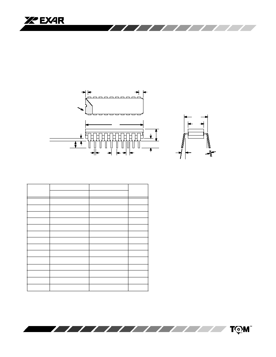
A
≠≠
0.200
≠≠
5.08
≠≠
b
0.014
0.023
0.356
0.584
≠≠
b
1
0.038
0.065
0.965
1.65
2
c
0.008
0.015
0.203
0.381
≠≠
D
≠≠
1.060
≠≠
26.92
4
E
0.220
0.310
5.59
7.87
4
E
1
0.290
0.320
7.37
8.13
7
e
0.100 BSC
2.54 BSC
5
L
0.125
0.200
3.18
5.08
≠≠
L
1
0.150
≠≠
3.81
≠≠
≠≠
Q
0.015
0.070
0.381
1.78
3
S
≠≠
0.080
≠≠
2.03
6
S
1
0.005
≠≠
0.13
≠≠
6
0
∞
15
∞
0
∞
15
∞
≠≠
D
b
e
1
b
20 LEAD CERAMIC DUAL-IN-LINE
(300 MIL CDIP)
D20
SYMBOL
MIN
MAX
MIN
MAX
NOTES
INCHES
MILLIMETERS
S
1
S
NOTES
1.
Index area; a notch or a lead one identification mark
is located adjacent to lead one and is within the
shaded area shown.
2.
The minimum limit for dimension b
1
may be 0.023
(0.58 mm) for all four corner leads only.
3.
Dimension Q shall be measured from the seating
plane to the base plane.
4.
This dimension allows for off-center lid, meniscus and
glass overrun.
5.
The basic lead spacing is 0.100 inch (2.54 mm) be-
tween centerlines.
6.
Applies to all four corners.
7.
This is measured to outside of lead, not center.
20
1
10
11
See
Note 1
E
c
E
1
L
Q
Seating
Plane
Base
Plane
L
1
A